
High Frequency VCO Design and Schematics
Iulian Rosu, YO3DAC / VA3IUL,
This note will review the process by which VCO (Voltage Controlled Oscillator) designers choose
their oscillator’s topology and devices based on performance requirements, components types and DC
power requirements.
Basic oscillator design specifications often require a given output power into a specified load at the
design frequency. The drive level and bias current set the fundamental output current and the oscillation
frequency is set by the resonator components.
Transistor selection of the transistor should consider noise, frequency, and power requirements.
Based on the particular device, the design may account for parasitics of the device affecting resonator
components as well as nonlinear performance specifications.
All the VCO schematics presented below were practical build using the Infineon SiGe transistor BFP420,
and any of them can be re-tuned for different frequency ranges changing varicaps and LC tank values.
VCO Specifications
•
The VCO must exhibit a low Phase Noise in order to meet the Sensitivity, Adjacent Channel and
Blocking requirements. In digital modulation scheme the VCO’s Phase Noise affects the Bit Error
Rate requirements. High Pushing (change of the oscillation frequency with supply voltage) can
cause Phase Noise degradation due to increased sensitivity to the power supply noise.
Phase Noise varies typically by 3dB with temperature, in the –55ºC to +85ºC range.
•
A buffer at the output is necessarily to isolate the VCO from any output load variations (Pulling) and
to provide the required output power. Meeting simultaneously the output power and load pull
specification directly with a stand-alone oscillator would be difficult. However, this buffer amplifier
requires a higher supply current. Alternative would include to use at the output circulators, isolators
or passive attenuators.
•
VCO output power is usually measured into a 50 ohm load. Output power requirements specified in
dBm, and tolerances vs tuning frequency in ± dB.
•
The tuning slope is the slope of the frequency to voltage tuning characteristic at any point and is the
same as modulation sensitivity. The slope could be positive or negative. For a positive slope, the
output frequency. increases as the tuning voltage increases. Similarly for a negative slope, the output
frequency decreases as the tuning voltage increases
•
A monotonic tuning characteristic means that the frequency is single valued at any tuning voltage
and that the slope has the same sign across the tuning range.
•
Tuning sensitivity as a function of tuning voltage is a measure of tuning linearity. For any given
application, have to specify the minimum and maximum of the tuning sensitivity. In the case of a
VCO, the frequency coverage is rather restricted since the influence of the feedback network is small
compared to the active device itself. Conventional oscillator designs (with a LC circuit or
transmission-line equivalent coupled to a negative-resistance active device will only provide a
restricted frequency coverage and poor stability). A negative resistance can easily be obtained from
most microwave transistors when considering chip and package parasitics.
•
Tuning flatness - As the VCO frequency range is increased, the difficulty to achieve a flat output
power is increased. Adding an output filter to suppress harmonics may in some
cases degrade power
output flatness.
•
The drive level should consider the trade-off between harmonic content, oscillator stability, and
noise.

In order to lower the VCO Phase Noise, a number of rules should be respected:
•
The active device has noise properties which generally dominate the noise characteristic limits of an
oscillator. Since all noise sources, except thermal noise, are generally proportional to average
current flow through the active device, it is logical that reducing the current flow through the device
will lead to lower noise levels.
•
Narrowing the current pulse width in the active device will decrease the time that noise is present in
the circuit and therefore, decrease Phase Noise even further.
•
Maximize the loaded Q of the tuned circuit in the oscillator.
There is a trade-off between the Q factor of the oscillator, its size and its price. The low Q-Factor of
an LC tank and its component tolerances needs careful design for phase noise without individual
readjustment of the oscillators.
Usually a larger resonator will have a higher Q (e.g. a quarter wavelength coaxial resonator).
•
Choose an active device that has a low flicker corner frequency.
A bipolar transistor biased at a low collector current will keep the flicker corner frequency to a
minimum, typically around 6 to 15 KHz (Most semi-conductor manufacturers can provide the
frequency corner (fc) of their devices as well as the 1/f characteristic.
•
Maximize the power at the output of the oscillator.
In order to increase the power at the input of the oscillator, the current has to be increased. However,
a low current consumption is critical to preserving battery life and keeping a low fc. In a practical
application, the current will be set based on output power required to drive the system (typically a
mixer), and then the Phase Noise will need to be achieved through other means.
•
Choose a varactor diode with a low equivalent noise resistance.
•
The varactor diode manufacturers do not measure or specify this parameter. The best approach is
then empirical; by obtaining varactors from several vendors and experimentally finding out which one
yields the lowest phase noise in the VCO circuit and thus has the lowest equivalent noise resistance.
•
There are two basic types of varactors: Abrupt and Hyperabrupt.
- The abrupt tuning diodes will provide a very high Q and will also operate over a very wide tuning
voltage range (0 to 60 V). The abrupt tuning diode provides the best phase noise performance
because of its high quality factor.
- The hyperabrupt tuning diodes, because of their linear voltage vs. capacitance characteristic, will
provide a much more linear tuning characteristic than the abrupt diodes. These are the best choice
for wide band tuning VCO's. An octave tuning range can be covered in less than 20 V tuning range.
Their disadvantage is that they have a much lower Q and therefore provide a phase noise
characteristic higher than that provided by the abrupt diodes.
•
Keep the voltage tuning gain (Ko) to the minimum value required.
This is the most challenging compromise because the thermal noise from the equivalent noise
resistance of the varactor works together with the tuning gain of the VCO to generate phase noise.
This compromise will be the limiting factor determining the phase noise performance.
•
Noisy power supplies may cause additional noise. Power supply induced noise may be seen at
offsets from 20 Hz to 1 MHZ from the carrier. If the VCO is powered from a regulated power supply,
the regulator noise will increase depending upon the external load current drawn from the regulator.
The phase noise performance of the VCO may degrade depending upon the type of regulator used,
and also upon the load current drawn from the regulator. To improve the phase noise performance of
the VCO under external load conditions it is always a good design philosophy to provide RF
bypassing of power and DC control lines to the VCO. RF chokes and good bypassing capacitors (low
ESR) is recommended at the DC supply lines. This will minimize the possibility of feedback between
stages in a complex subsystem. Improved bypassing may be provided by incorporating an active
filter
circuit.
VCO Topologies
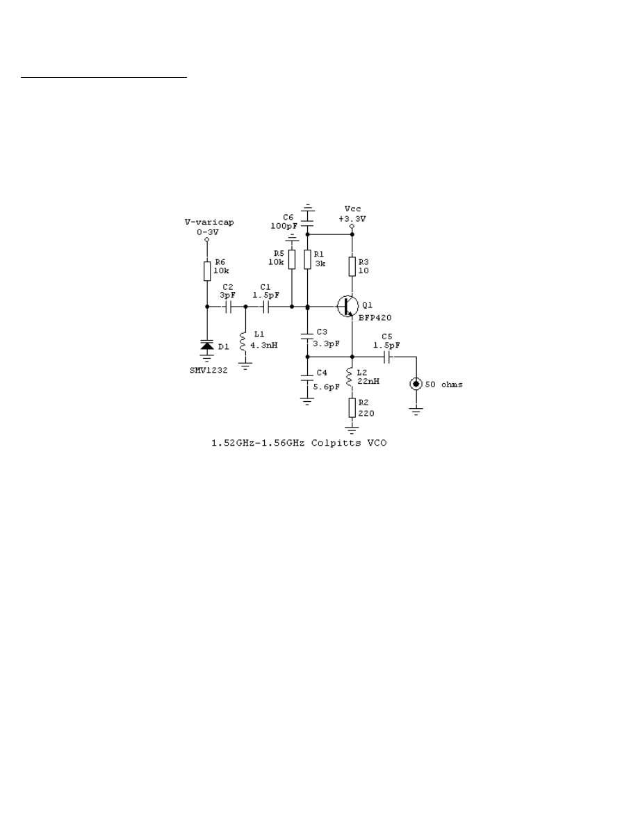
Parallel Tuned Colpitts VCO
There are 3 types of BJT Colpitts VCOs. Common-Collector, Common-Emitter and Common-Base.
The most used is Common-Collector configuration where the output is often taken from the collector
terminal, simply acting as a buffer for the oscillator connection at the base-emitter terminals.
This is the only Colpitts arrangement in which the load is not part of the three-terminal model or the
oscillator equation; though care must be taken to ensure that the collector output voltage does not
significantly feedback through the base-collector junction capacitance.
As an alternative, the output of the common collector could also be taken across emitter resistance Re.
•
The ratio of the feedback capacitors in the Colpitts VCO (C3 and C4), is more important than the
capacitor’s actual values. A good place to start is with a one to one ratio. The loaded Q of the
resonator circuit can be increased by reducing C3 or increasing C4. Doing so however, reduces the
loop gain in the oscillator, and enough loop gain must be maintained to guarantee oscillation start-up
under all conditions (mainly under different temperatures and system output loads).
•
The value of the collector resistor, R3 affects the oscillator loop gain. As in a common collector
amplifier, the lower the impedance in the collector circuit the more loop gain the circuit will have. This
resistor provides another means of controlling the loop gain of the oscillator since a good oscillator
design has just enough loop gain to guarantee reliable oscillation start-up. If there is to much loop
gain the oscillator will operate in deep compression which will load the Q of the resonator circuit
because the input impedance at the base of the transistor is very low when current saturation occurs.
The resistor also tends to minimize the level of the harmonics.
•
L2 is chosen as an RF choke to provide a high impedance in the emitter circuit and ensure that most
of the oscillator power is fed back to the base of Q1 instead of being dissipated in R2.
•
Emitter resistor R2 is used for current feedback thus providing a stable DC bias point that will be
independent of the beta of the transistor.
•
C1 capacitor defines the amount of coupling between the active device and the resonator. The lighter
the coupling (a smaller value of C1), the better the loaded Q of the resonator is, which results in a
better phases noise performance. However, the compromise is a reduced output power and the
potential for the VCO not to start under all operating conditions (especially at higher temperatures
when current gain is reduced). Designing the system with too light of a coupling may also results in a
sensitive design which may yield potential manufacturing problems.
•
The final tuning component of the oscillator, C2 sets the voltage tuning gain of the oscillator. This
capacitor should keep the coupling as light as possible while maintaining the required frequency
tuning range of the VCO so that the varactor’s phase noise contribution is reduced to a minimum. If
the coupling is too light, the oscillator may not start under certain conditions. The worst case
condition for this oscillator topology is when V-varicap is set at zero volts.
•
A good way to check if C2 is large enough for reliable oscillator start up is to monitor the output
power of the VCO with zero volts on the tune line. The power with V-varicap at 0V should be within 1
dB of the power with V-varicap at 3V. If C2 is too small, the output power of the VCO will fall off
sharply when V-varicap approaches zero volts or the oscillator may stop completely.
•
One good reason to use a transistor with a high Ft such as the BFP420 (Ft = 25GHz) is that C2 can
be small and oscillation start-up will be reliable simultaneously.
•
In order to ensure that the loaded Q of the resonator circuit is not the limiting factor in phase noise
performance, the varactor can be replaced with a fixed 2.5pF capacitor and compare the results. A
varactor can degrade up to 5-6dB
•
The varactor can reduce the Q of the resonator circuit but this effect is secondary to the varactor
modulation due to its own equivalent noise resistance. One way of reducing this effect is to parallel
two or more varactors of smaller value while keeping the same tuning curve. This effectively reduces
the equivalent noise resistance.
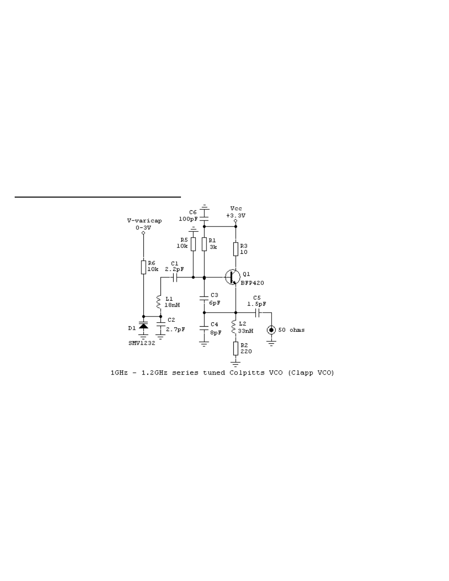
Series Tuned Colpitts VCO (Clapp VCO)
The series-tuned Colpitts circuit (or Clapp oscillator) works in much the same way as the parallel one.
•
The difference is that the variable capacitor, C1, is positioned so that it is well-protected from being
swamped by the large values of C3 and C4.
•
In fact, small values of C3, C4 would act to limit the tuning range. Fixed capacitance, C2, is often
added across the varicap to allow the tuning range to be reduced to that required, without interfering
with C3 and C4, which set the amplifier coupling.
•
The series-tuned Colpitts has a reputation for better stability than the parallel-tuned original. Note
how C3 and C4 swamp the capacitances of the amplifier in both versions.
•
The oscillation frequency is given by:
ω
2
L = [1/(C2+Cvar)]+(1/C3)+(1/C4)
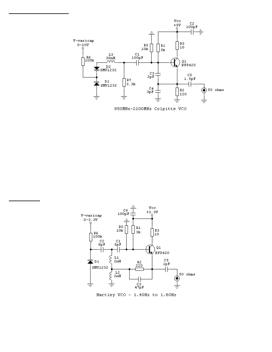
Wideband Colpitts VCO
•
This wideband Colpitts VCO uses a series back-to-back connection of two SMV1232 varactors
instead of a single varactor. This connection allows lower capacitance at high voltages, while
maintaining the tuning ratio of a single varactor. The back-to-back varactor connection also helps
reduce distortion and the effect of fringing and mounting capacitances.
•
The wideband Colpitts feedback capacitances C3, C4 were optimized to provide a flat power
response over the wide tuning range. These values may also be re-optimized for phase noise if
required.
•
The circuit is very sensitive to the transistor choice (tuning range and stability) due to the wide
bandwidth requirement.
•
DC bias is provided through resistors R6 and R7, which may affect phase noise, but allows the
exclusion of RF chokes. This reduces costs and the possibility of parasitic resonances which is the
common cause of spurious responses and frequency instability.
Hartley VCO
•
The Hartley VCO is similar to the parallel tuned Colpitts, but the amplifier source is tapped up on the
tank inductance instead of the tank capacitance. A typical tap placement is 10 to 20% of the total
turns up from the “cold” end of the inductor. (It’s usual to refer to the lowest-signal voltage end of an
inductor as cold and the other, with the highest signal voltage as hot.). The same as in Colpitts case
a good place to start is with a one to one ratio.
•
C2 limits the tuning range as required.
•
C1 is reduced to the minimum value that allows reliable starting. This is necessary because the
Hartley’s lack of the Colpitts’s capacitive divider would otherwise couple the transistor capacitances
to the tank more strongly than in the Colpitts, potentially affecting the circuit’s frequency stability.
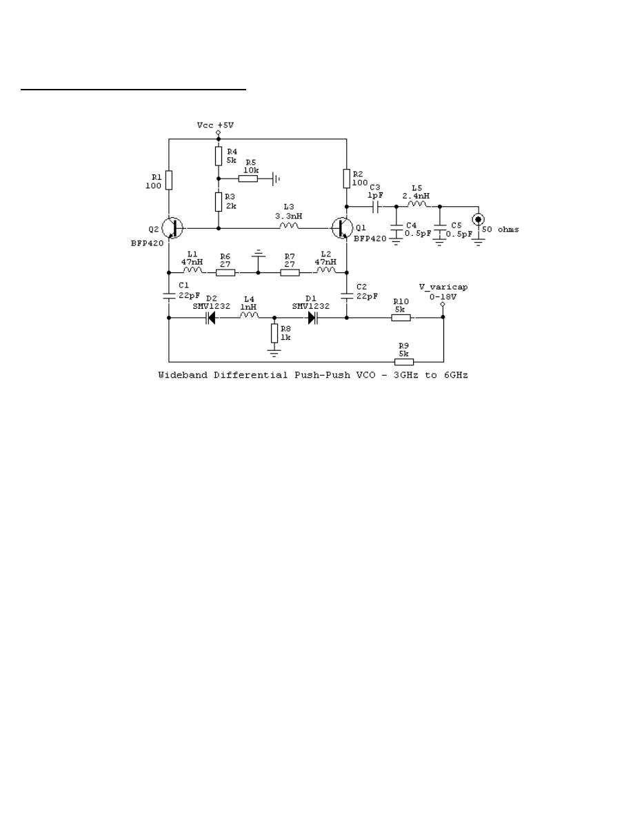
Wideband Differential Push-Push VCO
•
The circuit schematic shows a pair of transistors in a single feedback loop, connected so that
collector currents would be 180° shifted. A pair of back-to-back connected SMV1232 varactors is
used to allows lower capacitance at the high voltage range, without changing the tuning ratio.
•
Varactor DC biasing is provided through resistors R8, R9 and R10, which may affect the phase
noise, but eliminate the need for inductive chokes. This eliminates the possibility of parasitic
resonances that could affect the wide tuning range and also cause for frequency instability and
spurs.
•
The DC chokes, L1 and L2 are used for phase correction between pairs and their losses is
dominated by the series emitter resistors R6 and R7.
•
The DC blocking series capacitances C1 and C2, including associated parasitics, shall have the SRF
outside of the tuning range.
•
A three-pole Low Pass Filter at the output is used to filter the unwanted spurious.
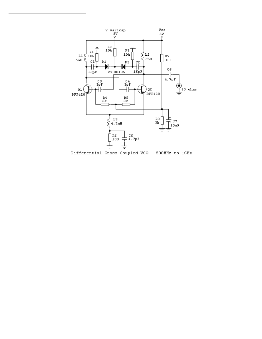
Differential Cross-Coupled VCO
The cross-coupled differential transistor pair presents a negative resistance to the resonator due to
positive feedback.
This negative resistance cancel the losses from the resonator enabling sustained oscillation.
Frequency variation is achieved with two varicap diodes BB135.
•
An optimal trade-off between thermal noise- induced phase noise and DC power dissipation can be
achieved when the oscillation amplitude is designed to set the differential pair transistors to operate
at the boundary between saturation and linear regions.
•
The excess noise factor F is dominated by the noise from the tail current source near even
harmonics of the carrier frequency. In order to improve phase noise this contribution has to be
minimized. An efficient way of doing this is to use a noise filtering technique. An inductor L3 and
capacitor C5 forms a 2nd order low-pass filter which prevents noise at even harmonics from being
injected into the feedback path of the oscillator.
•
The noise filter leaves low-frequency noise from the tail current source unaffected. Low-frequency
noise from the tail current source is also up-converted to the carrier as amplitude modulation. Low-
frequency noise on the tuning line modulates the non-linear capacitance of the varactors giving rise
to phase noise variation with control voltage.
•
The phase noise degradation due to control voltage noise is very significant at the lower tuning range
where the varactors are most non-linear. The stack of two varactors reduces the varactor gain Kvco
at the lower tuning range which in turn reduces phase noise variation with control voltage.
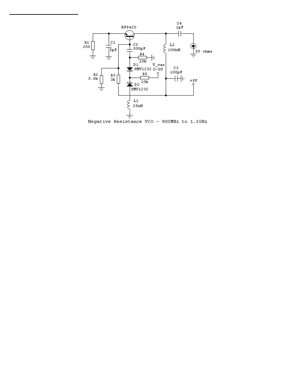
Negative Resistance VCO
•
The resonator of the Negative Resistance VCO is a series-tuned base network consisting of two
series varicap capacitances and an inductor for the positive reactance element.
•
Performance is highly dependent on the transistor type. Certain component values are critical.
•
This oscillator actually works best when lower Ft transistors are used. The circuit can be envisioned
as a series-tuned Clapp, with internal transistor base-to-emitter capacitance and collector-to-emitter
capacitance acting as a voltage divider. Microwave transistors with little internal capacitance do not
work well except at the high end of the useful range of this oscillator type. Higher Ft devices required
increased capacitance added at the emitter. At the low end of the frequency range, adding external
base-to-emitter capacitance is sometimes necessary,
•
If bias conditions result in a emitter resistance below about 200 ohms, an RF choke may be required
in series with the resistance. This choke must be free of any resonances in the operating frequency
range.
•
The output can be taken from several points. The L1 inductor can be tapped. As the tap is moved
toward the transistor, more power is coupled out. If the tap is too close to the transistor, the loading
reduces the oscillation margin, and the operating frequency becomes more load dependent.
The output can be taken by capacitive coupling at the emitter (low level) or at the collector (higher
level, but have more spurious).
•
Because the negative resistance oscillator uses a series-tuned resonator, the varactors lead
inductance becomes a part of the resonator. This is an advantage over varactor-tuned oscillators
using parallel resonators. The base coupling capacitor inductance and transistor base inductance are
also absorbed.
•
The loaded Q of negative resistance oscillators is typically less than 5 and this circuit defies attempts
at improving the Q. When used as a broadband varactor-tuned VCO, the low loaded Q does not limit
phase noise performance significantly because varactor modulation noise predominates, particularly
at higher offset frequencies.
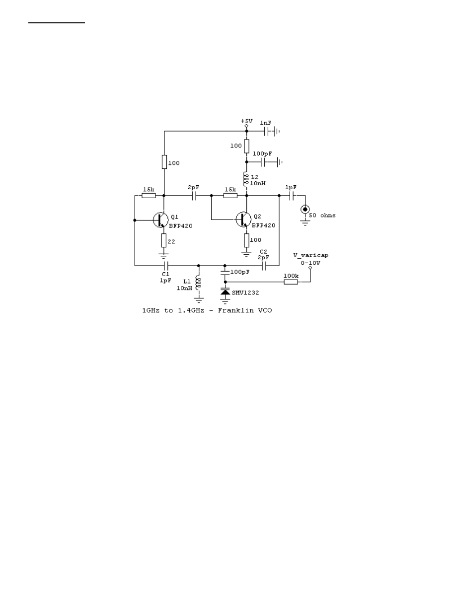
Franklin VCO
Franklin oscillator uses two transistor stages having the same common terminal (emitter for bipolar
device) when the greater power gain and better isolation from the resonant circuit is possible compared
with the case of a single-stage configuration.
There are two possible configurations for the resonant circuit, parallel and series.
The circuit presented below uses a parallel LC resonant circuit (L1 and the varctor diode).
In the case of a parallel resonant circuit configuration, the resonant LC circuit is isolated from the
input of the first stage and the output of the second stage by means of small shunt capacitances C1 and
C2 having high reactances at the resonant frequency.
In this circuit, each stage shifts phase 180° so that the total phase shift is 360° which is equivalent to
zero phase shift. We may say that one stage serves as the phase inverting element in place of the RC
or LC network which generally performs this function. It is, from an analytical viewpoint, immaterial which
stage we choose to look upon as amplifier or phase inverter.
The configuration is essentially symmetrical in this respect; both stages provide amplification and
phase inversion.
•
The salient feature of the Franklin oscillator is that the tremendous amplification enables operation
with very small coupling to the resonant circuit.
•
Therefore, the frequency is relatively little influenced by changes in the active device, and the Q of
the resonant circuit is substantially free from degradation.
•
The closest approach to the high frequency stability inherent in this oscillator is attained by restriction
of operation to, or near to, the Class-A region. This should not be accomplished by lowering the
amplification of the two stages, but, rather by making the capacitors C1 and C2 very small.
•
Additionally, a voltage-follower 'buffer' stage is helpful in this regard. Extraction of energy directly
from the resonant tank, would, of course, definitely negate the frequency stability otherwise
attainable.
•
Obviously, the Franklin oscillator is intended as a low-power frequency-governing stage, not as a
power oscillator.
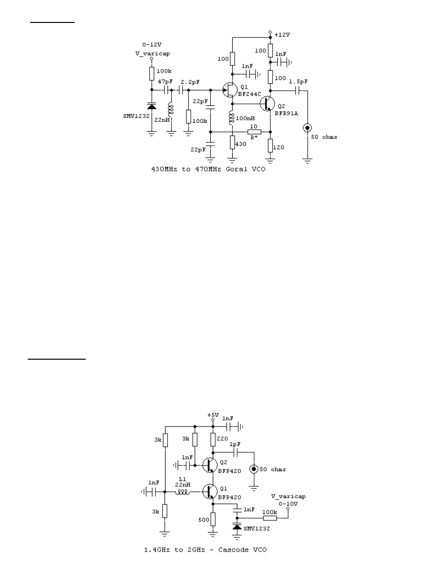
Goral VCO
The Goral VCO has an emitter-follower stage inserted in the feedback path of an otherwise
conventional Colpitts oscillator circuit.
•
The midpoint of the capacitive divider (which is actually part of the resonant tank) now sees a
much lower impedance with respect to ground than would be the case without the emitter
follower.
•
Because the feedback gain of a Goral VCO is greater than a standard Colpitts, placing a
feedback resistor R*, helps improving the overall phase noise performance and improving also
the linearity, reducing the VCO generated harmonics.
•
The power gain of the JFET/BJT combination is much greater than that of the JFET 'oscillator'
alone. There is latitude for considerable experimentation in the ratio of the two capacitors used in
the Colpitts section of the circuit. This ratio can be optimized for frequency stability without easily
running out of feedback.
Note that the emitter-follower is directly coupled to the JFET. It may be necessary to experiment with
bias-determining resistances to ascertain Class-A operation from the emitter-follower. Also, the output
transistor is intended to operate in its Class-A region.
Cascode VCO
To provide higher isolation of the load from the VCO resonant circuit a cascode VCO configuration, can
be used.
The negative resistance oscillation conditions for common emitter transistor Q1 are provided by using
the feedback inductance L1.
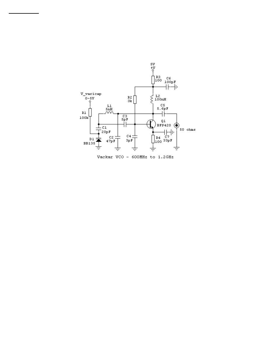
Vackar VCO
And here is the winner. If you want to build a very stable, low phase noise, and low spurious VCO,
definitely Vackar VCO is the choice.
This is not a common type in the RF “professional” world, one reason could be the name of its inventor.
A Vackar VCO is a variation of the split-capacitance oscillator model. It is similar to a Colpitts or Clapp
VCO in this respect. It differs in that the output level is more stable over frequency, and has a wider
bandwidth when compared to a Colpitts or Clapp design.
The Vackar VCO circuit incorporates a
π-section tank to attain the needed 180° phase-reversal in the
feedback loop.
•
However, the inverted feedback signal is not directly fed back to the input of the active device; rather,
it is loosely coupled through a small capacitor. Often, a shunt capacitor is introduced to further
reduce the coupling.
•
The basic idea is to isolate the resonant circuit as much as possible from the input of the active
device, consistent with obtaining reliable oscillation.
•
This circuit is particularly advantageous with solid-state devices, and especially with bipolar
transistors that have inordinately-low input impedances and that present a widely-varying reactance
to the tuned circuit as a consequence of temperature and voltage changes.
•
Once the overall circuit is operational, the values of capacitance C1 in series with C
var
and collector
capacitance (C2) may be optimized for best stability. Generally, it will be found that the capacitor
closest to the collector of the transistor can be several times larger than the capacitor associated with
the base circuit.
•
The introduction of attenuation in the feedback loop (via the small capacitor in the Vackar) prevents
over-excitation and effectively isolates the resonant circuit from the active device.
•
The frequency tuning range of Vackar VCO is above one octave, not observable to many oscillator
types.
•
The frequency tuning is provided independently of the coupling to the LC tank circuit.
•
The parametric variables of the transistor (which depends by the bias current and temperature), are
isolated from the resonator.
•
The transistor input is not overloaded as other VCO circuits and the collector output has low
impedance providing low gain just to maintain the oscillation.
•
The feedback division ratio is fixed (typical range for coupling ratio is 1:4 up to 1:9). Even if the VCO
is tuned, the impedance divider is fixed, in this way increasing the stability.
•
Two negative sides of Vackar VCO are the critical starting oscillation point, and the low output level,
which always requires using a buffer amplifier. When the oscillation doesn’t start means that it

doesn’t have enough positive feedback, as for to begin the oscillation and maintain it in the time. In
the above schematic C3 and C4 are critical values finding this point.
•
L2 is used as an RF choke with SRF outside of the frequency range, to don’t affect the tuning range
and flatness over frequency. It is important that the RF choke in the collector circuit 'looks good' at
the operating frequency (presents a high inductive reactance). Resonances from distributed
capacitance in the choke windings, especially those in the series-resonant mode, can degrade
stability or even inhibit oscillation. Ferrite-core chokes are generally suitable for this application.
•
Sensitivity to RF choke characteristics is common to all oscillator circuits that use chokes for shunt-
feeding the DC operating voltage to the oscillator.
References:
1. Alpha Industries - VCO Application notes
2. Minicircuits - VCO Application notes
3. Oscillator Basics and Low-Noise Techniques for Microwave Oscillators and VCOs - U.Rohde
4. Oscillator Design and Computer Simulation - R.Rhea
5. RF and Microwave Transistor Oscillator Design – A. Grebennikov
6. Practical Oscillator Handbook - I. Gottlieb
7. RF Design Magazine - 1997 - 2003
8. Microwave Journal - 1997 - 2008
9. Microwaves & RF - 2002 - 2006
Wyszukiwarka
Podobne podstrony:
Synchronous Generator And Frequency Converter In Wind Turbine Applications System Design And Efficie
VCO designs for wireless handset and catv
US Patent 568,179 Method Of And Apparatus For Producing Currents Of High Frequency
De Matos And Fernandes Testing The Markov Property With Ultra High Frequency Financial Data
Thomas And Patnaik Serial Correlation In High Frequency Data And The Link With Liquidity
Ito And Hashimoto High Frequency Contagion Of Currency Crises In Asia
Zied H A A modular IGBT converter system for high frequency induction heating applications
9 Guidelines for Fiber Optic Design and Installation
Lab 6, 9.2.1.5 Packet Tracer - Designing and Implementing a VLSM Addressing Scheme Instruct
Monitoring the Risk of High Frequency Returns on Foreign Exchange
DB Systems Super High Grade Pre amp and DB 4 Moving Coil Cartridge Pre Amp
Ir2111 High Voltage High Speed Power Mosfet And Igbt Driver
khuller design and analyze algorithms 65HVWXZDMCYAU3QEPBSDD6TGRTHF3UH7L2EEOGA
Design and performance optimization of GPU 3 Stirling engines
DB Systems Super High Grade Pre amp and DB 4 Moving Coil Cartridge Pre Amp
SSP 406 DCC Adaptive Chassis Control Design and Function
Design and implementation of Psychoacoustics Equalizer for Infotainment
DESIGN AND DEVELOPMENT OF MICRO TURBINE
więcej podobnych podstron