
Alpha Industries, Inc. [781] 935-5150
• Fax [617] 824-4579 • Email sales@alphaind.com • www.alphaind.com
1
Specifications subject to change without notice. 8/99A
VCO Designs for Wireless Handset and
CATV Set-Top Applications
APN1012
Introduction
Voltage Controlled Oscillators (VCOs) have come to the
forefront of RF designs together with the first PLL circuits.
In the era before the PLL, oscillators were mostly free
running and only in rare cases were varactors used for
modulation or temperature compensation. Nowadays, we
rarely see free running oscillators, instead they have
become varactor controlled oscillators. This is because
most RF applications require band coverage, which can
be realized through the PLL circuit requiring two sources
of RF power. The reference source frequency is often a
VCXO or TCXO, while the other frequency is controlled
by the PLL phase detector.
Usually, both VCXO/TCXO and the RF VCO are voltage
controlled oscillators. The difference between a reference
oscillator and a tuned VCO is that the former usually has
a very high-Q resonator, which allows for very stable
Application Note
oscillation, while the latter has a lower-Q resonator,
allowing a relatively high tuning range. In reference
oscillators, varactors are used for fine tuning or
temperature compensation (TCXO). In tunable oscillators,
varactors are used to change (tune) the frequency. In
some VCOs, varactors may be used also for modulation,
for example in a DECT system where modulation is used
to generate a constant-envelope GMSK signal.
Although it is a small part of the RF design, the VCO is
often a major headache for designers. The goal, in this
application note, is to show how Alpha’s products and
services may help you to overcome VCO concerns and
help to make your design among the best products
on the market.
2
Alpha Industries, Inc. [781] 935-5150
• Fax [617] 824-4579 • Email sales@alphaind.com • www.alphaind.com
Specifications subject to change without notice. 8/99A
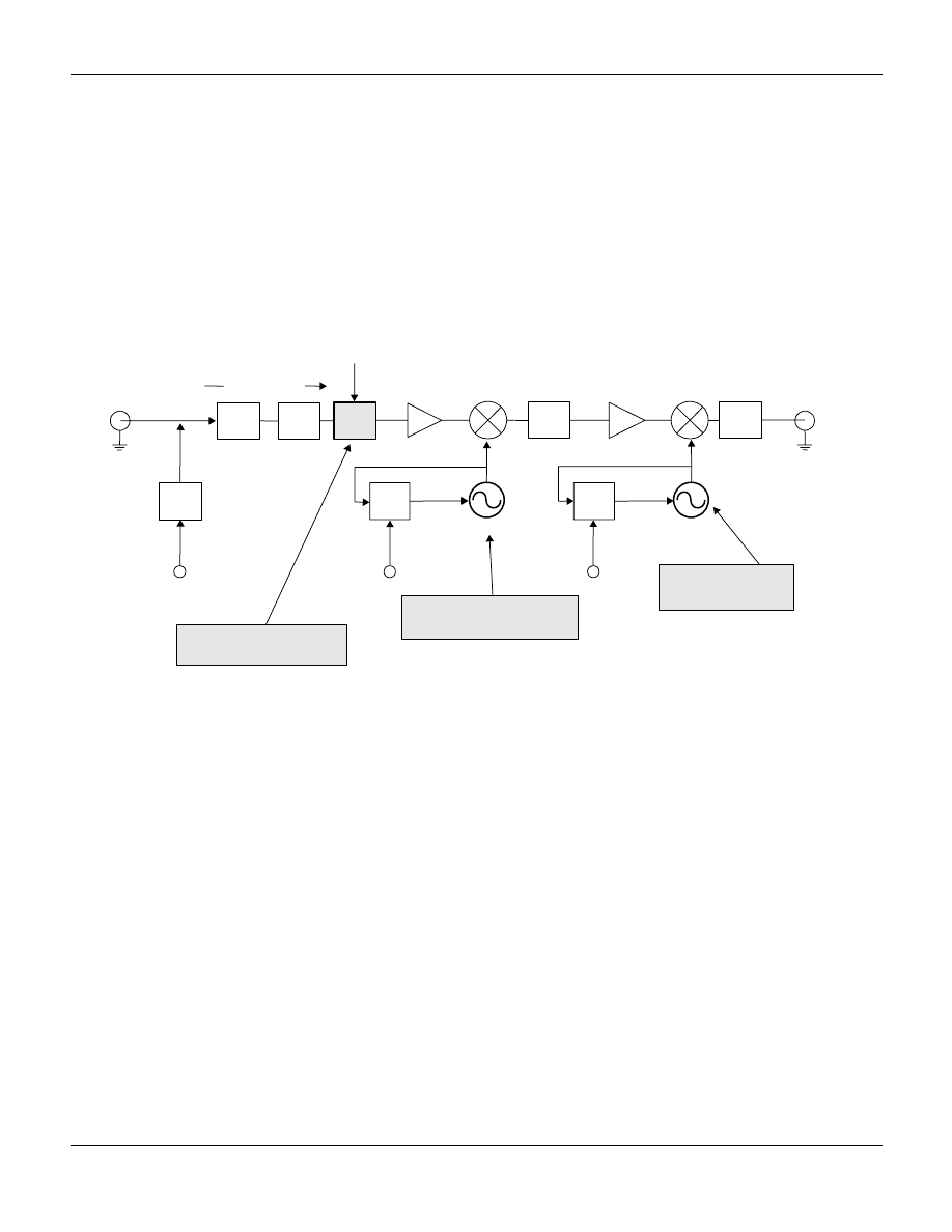
VCOs in Digital Wireless Phones
Consider the hypothetical wireless handset phone.
Today, the handset is a dual-band (cellular/PCS) and multi-
mode system employing many VCO functions. There are
many ways to realize these functions, making it virtually
impossible to specify the frequency and tuning range for
all designs. However, there are certain common features
that are outlined in Figure 1.
In a typical receiver, dual conversion superheterodyne
solutions are usually employed. They convert either
900 MHz (cellular) or 1.8 GHz (PCS) down to the SAW
frequency range, which may be between 90–400 MHz.
Further, this signal is either down-converted or
demodulated into a digital I/Q signal using a lower
frequency IF VCO. The transmitter path is either directly
modulated at 900 MHz or uses a dual conversion scheme
requiring at least two VCOs.
When dual-band requirements are needed, up to 8 or
more VCOs may be required to satisfy specific frequency
plans. This is often a technically and economically
restrictive solution. Many designers try to solve this over-
VCOed problem using both smart frequency planning and
multi-band VCOs, as shown in Figure 1.
VCO Designs for Wireless Handset and CATV Set-Top Applications
APN1012
RF VCO Ranging:
400–1900 MHz
T/R
Switch
I
IF VCO
RF VCO
BPF
BPF
BPF
BPF
LNA
RF
Detector
PA
BPF
PLL
Control
PLL
PLL
Control
PLL
π/2
Σ
BPF
PLL
Control
π/2
PLL
Control
PLL
I
Q
Q
RF VCO
IF VCO
Ranging:
100–400 MHz
PLL
Coupler
Figure 1. VCOs in a Digital Wireless Phone
Alpha Industries, Inc. [781] 935-5150
• Fax [617] 824-4579 • Email sales@alphaind.com • www.alphaind.com
3
Specifications subject to change without notice. 8/99A
Fundamental Low Noise Colpitts VCO
The characteristic feature of the Colpitts VCO is that it uses
a capacitive divider for the feedback consisting of C
1
and
C
2
, and an inductive branch including a parallel resonator
and series capacitor C
3
. The parallel resonator includes
inductive element M
1
(that may be a discrete inductor for
lower frequencies or a length of micro-strip line for RF) and
a capacitive branch, consisting of a varactor and a series
capacitor(s). The entire inductive branch should have
inductive impedance at the frequency of oscillation,
otherwise there will be no oscillation. This means that the
resonant frequency should be higher than the oscillation
frequency.
Note that the resonator current circulates through the
varactor, series capacitor C
11
and inductor M
1
and is the
largest current in the tank circuit. Because of this, losses
introduced in this current path are the crucial ones with
respect to phase noise.
Without delving deeply into phase noise theory, we note
that phase noise is inversely proportional to the power
bypassed through the feedback loop, and the loaded Q
of the tank circuit. Thus, the more power lost on the way
to the transistor base, the higher the noise. It is clear that
varactor loss plays a crucial role in the phase noise
property of the VCO. If phase noise is an issue, the
varactor series resistance should be carefully considered.
There is an additional concern because phase noise is not
only a function of varactor loss. The varactor capacitance
voltage characteristic has a crucial impact on phase noise
as well. With a higher capacitance ratio, the varactor’s
coupling to the resonator is reduced resulting in lower
resonator current. Therefore, a hyperabrupt varactor
having higher series resistance is often a better choice
than a lower capacitance ratio abrupt varactor having lower
series resistance.
VCO Designs for Wireless Handset and CATV Set-Top Applications
APN1012
Q
1
2SC5007 (“34”)
Q
2
2SC5008 (“44”)
C
1
2 p
C
2
1.5 p
C
3
0.75 p
C
7
0.5 p (0402)
R
1
150
R
2
2.7 k
C
4
0.75 p
C
8
R
3
200
R
4
3.6 k
C
5
0.75 p
C
6
0.75 p
M
1
4 x 04 mm (Trim)
D
1
SMV1493
C
10
15 p
C
11
1.5 p (0603)
C
9
C
12
1 p
M
2
6.5 x 0.2 mm
M
3
4 x 0.35 mm
V
TUNE
M
4
2 x 0.2 mm
M
6
5 x 0.2 mm
M
5
2 x 0.2 mm
RF Out
V
CC
Low R
S
, Low Voltage
Hyperabrupt Varactor
Figure 2. Low Noise High Performance Colpitts VCO
4
Alpha Industries, Inc. [781] 935-5150
• Fax [617] 824-4579 • Email sales@alphaind.com • www.alphaind.com
Specifications subject to change without notice. 8/99A
Differential VCO for Integration with
a RF IC
Designs based on RF IC solutions, with built-in VCOs,
often employ a differential VCO configuration. One
possible differential VCO configuration is shown in Figure
3. In this case, the tank circuit is formed by C
3
, C
4
and a
resonator C
8
, C
9
, D
1
, M
1
. Here again, the resonator
current plays a decisive role in phase noise definition.
Thus, phase noise is strongly dependent on resonator
loss. Capacitors C
3
and C
4
help establish the correct
phase shift value in the feedback loop moving oscillations
closer to the resonant frequency. This is the principal
difference between a Colpitts and a differential VCO. In
the Colpitts case, the resonant frequency is always higher
than the oscillation frequency; in the differential VCO the
resonant and oscillation frequencies may coincide. Thus
the loaded Q of the circuit becomes significantly higher,
and the feedback loop losses are increased due to the
higher resonant currents. When this happens, the
differential VCO is more vulnerable to resonator loss than
the Colpitts VCO and usually shows 5–10 dB higher noise
if compared to an equivalent Colpitts case.
VCO Designs for Wireless Handset and CATV Set-Top Applications
APN1012
V
1
V
2
V
3
R
1
47
R
2
3 k
R
3
9.1 k
R
4
3 k
R
5
3 k
R
6
3 k
R
7
3 k
R
8
20
R
9
3.9 k
L
1
33 n
C
1
100 p
C
2
2 p
C
3
4 p
C
4
1.5 p
D
1
SMV1493-079
C
5
1.5 p
C
6
100 p
C
7
100 p
V
CC
+3 V
V
VAR
RF Out
C
8
2 p
C
9
6 p
M
1
4 x 0.5 mm
M
2
6.5 x 0.2 mm
R
10
51
Low R
S
, Low Voltage
Hyperabrupt Varactor
RF IC
Figure 3. Differential VCO for the Integration with the RF IC
Alpha Industries, Inc. [781] 935-5150
• Fax [617] 824-4579 • Email sales@alphaind.com • www.alphaind.com
5
Specifications subject to change without notice. 8/99A
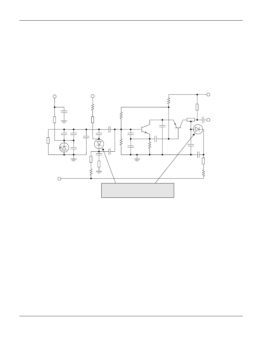
Dual-Band Switchable VCO Schematic
One way to improve design economics in the multi-VCO
requirement is to employ band switching in the VCO. If the
frequency switching required isn’t very large (say within
20%) it may usually be realized within the same tank
circuit, by switching “on” or “off” an additional capacitor or
inductor. However, if the required switching is more than
30%, it becomes very difficult to satisfy both wideband and
low noise requirements in a single design. One possible
solution is to use two separate tank resonator circuits
switched with two PIN diodes. In this case, the feedback
needs to be optimized to fit both band requirements at the
same time. Thus, a trick is used — connecting a capacitor
C
11
in parallel with C
6
when a lower-band resonator is
selected. This provides significant improvement in phase
noise since C
6
may then be optimized for the best
performance at high band, and C
11
at the lower band.
Another important feature of this switching scheme is that
the PIN diodes are not in the resonator current path.
Because of this, phase noise is not sensitive to the PIN
diode resistance. This is fortunate, since it means less
forward current is needed. In addition, any noise on the
PIN diode bias current (common for the noisy digital
environment of today’s phones) would not cause
significant modulation noise.
VCO Designs for Wireless Handset and CATV Set-Top Applications
APN1012
L
1
12 nH
D
1
C
1
8 pF
C
2
470 pF
C
3
100 pF
C
6
20 pF
C
7
15 pF
R
1
300
R
2
R
3
P
1
L
2
56 nH
D
2
SMV1139-011
C
8
10 pF
R
4
1.5 k
P
2
SMP1320-011
1
J
1
V
TUNE
1
J
2
V
SW_High
1
J
3
V
SW_Low
C
4
100 pF
C
5
100 pF
Q
1
NE68519
C
9
100 pF
C
10
20 pF
R
5
100
R
6
3 k
R
7
6.8 k
1
J
4
V
CC
+3 V
1
J
5
RF
1.5 k
1.5 k
C
11
30 pF
C
CC
100 pF
SMV1408-011
SMP1320-011
Low Current Switching
PIN Diodes
Low R
S
, Low Voltage
Hyperabrupt Varactor
Figure 4. Dual-Band Switchable VCO Schematic
6
Alpha Industries, Inc. [781] 935-5150
• Fax [617] 824-4579 • Email sales@alphaind.com • www.alphaind.com
Specifications subject to change without notice. 8/99A
Dual-Band Switchable RF VCO
As mentioned before, relatively small (less than 20%)
frequency switching may be achieved inside the same tank
circuit by connecting or disconnecting capacitors (and
sometimes inductors). The PIN diode D
2
performs a tricky
task ¾ it adds more capacitance in parallel with the
existing parallel capacitance of the resonator, and also
adds more capacitance in parallel with the existing series
capacitor. This technique is used to overcome the problem
of increased resonator Q, when connecting additional
parallel capacitance, by decreasing it with higher series
capacitance. It allows D
2
to keep phase noise near its
optimum at both bands. Another PIN diode in the output
matching circuit tunes the buffer to a frequency doubler
mode when working in PCS band.
VCO Designs for Wireless Handset and CATV Set-Top Applications
APN1012
V
CC
(3 V)
RF Out
D
3
D
2
D
1
V
VAR
V
CTL1
V
CTL2
D
1
: SMV1493-079
D
2
, D
3
: SMP1322-079
PINs are Using in Both Resonator Tank
and Output Matching Circuits
Figure 5. Dual-Band Switchable RF VCO
Alpha Industries, Inc. [781] 935-5150
• Fax [617] 824-4579 • Email sales@alphaind.com • www.alphaind.com
7
Specifications subject to change without notice. 8/99A
VCOs in a Set-Top Cable Down-Converter
The typical set-top down-converter is a dual-conversion
receiver employing up-conversion and down-conversion
techniques to overcome image problems in a wideband
environment of 50–1000 MHz. In the dual up-/down-
conversion scheme, the problem of image channel and
input filtering virtually does not exist because there is no
signal at the image channel. The image channel is always
higher than the highest frequency of the cable signal.
Two RF VCOs are required for dual down conversion. The
first is a wideband VCO tuned from 1100–2000 MHz with
a control voltage from 1–20 V. The other is a narrow band
VCO, which may use a CDR, coaxial dielectric resonator,
at 1144 MHz. In a digital system the second IF signal
may be further demodulated, requiring an additional
44 MHz VCO.
The specific action of the wideband VCO is its wideband
tuning requirement. Let us consider some possible
solutions for the wideband VCO.
VCO Designs for Wireless Handset and CATV Set-Top Applications
APN1012
BPF
PLL
PLL
LPF
HPF
LPF
Upstream
filter
BPF
Upstream
PLL
Control
PLL
Control
AGC
1st Mixer
75
Ω
54–860 MHz
40 dB
45.75/44 MHz
1100 MHz
1154–1960 MHz
1144/1145 MHz
2nd Mixer
Low-Distortion PIN Diode
Attenuator
Wideband VCO Tuning in
1100–2000 MHz Range
Narrow-Band VCO
@ 1145 MHz
dB
Figure 6. VCOs in a Set-Top Cable Down-Converter
8
Alpha Industries, Inc. [781] 935-5150
• Fax [617] 824-4579 • Email sales@alphaind.com • www.alphaind.com
Specifications subject to change without notice. 8/99A
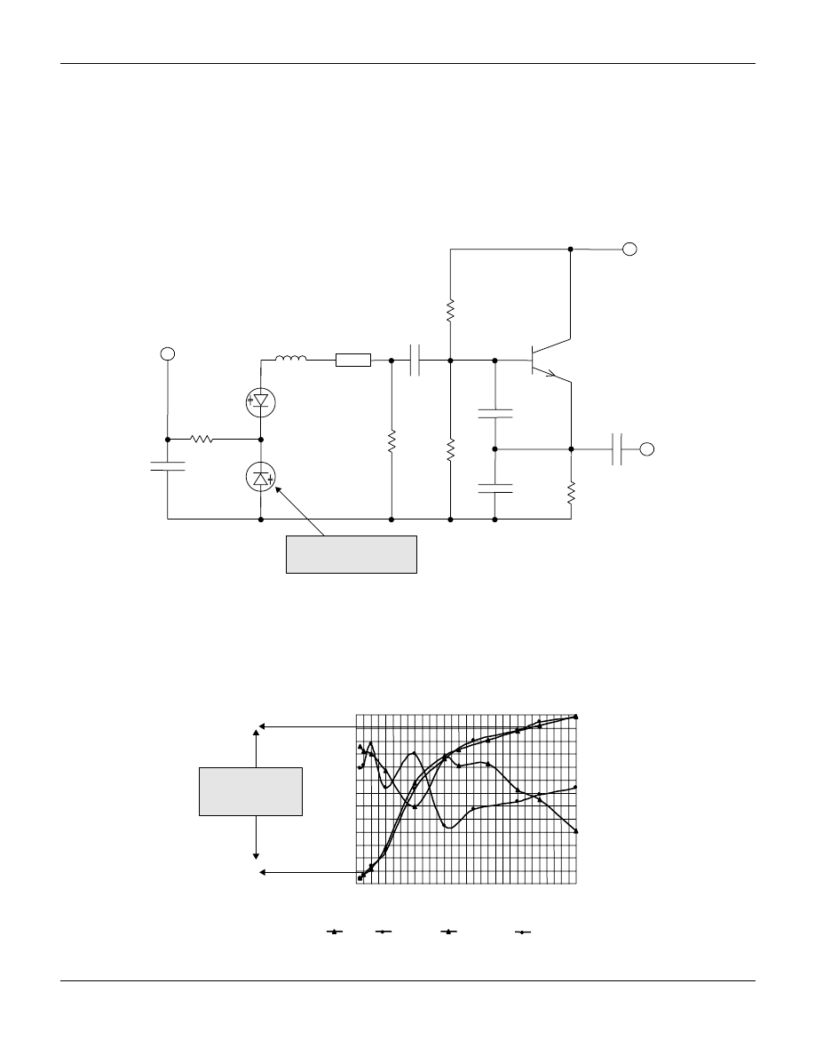
Wideband Colpitts VCO Schematic
The unique action of the wideband Colpitts VCO is in its
tank circuit design, which uses an inductor with a varactor
connected in series and no parallel capacitor in contrast
to the low noise Colpitts VCO described in Figure 7. The
feedback capacitors are optimized to the best power
flatness over the entire frequency band. Back-to-back
varactors are often used to minimize parasitic mounting
capacitance (between mounting pads and adjoining
components). This circuit is usually designed to minimize
any parasitic parallel capacitance that may be caused by
component pads or transmission lines close to the
inductive path.
VCO Designs for Wireless Handset and CATV Set-Top Applications
APN1012
V
CC
= 5 V
I
CC
= 9 mA
NE68519
SMV1265-011
3.3 k
9.1 k
200
3 k
3 k
320 x 30 mils
1 p
560 p
1.62 p
300 p
2 p
5.6 nH
SMV1265-011
RF Output
V
TUNE
High C (V) Ratio
Hyperabrupt Varactors
Useful Tuning
Range:
980–2120 MHz
0.9
1.0
1.1
1.2
1.3
1.4
1.5
1.6
1.7
1.8
1.9
2.0
2.1
2.2
0
5
10
15
20
25
30
Varactor Voltage (V)
Frequency (GHz)
P
OUT
(dBm)
0
1
2
3
4
5
6
7
Fexp
Fmodel
P
OUT
_exp
P
OUT
_model
A carefully designed layout with minimum parasitic
capacitances may show large frequency coverage, for
example 980–2120 MHz as the performance indicates.
The varactor selection is a crucial part of the design.
Alpha’s new SMV1265-011 varactor is specifically
designed to fit this wideband application.
Figure 7. Wideband Colpitts VCO Schematic
Figure 8. Wideband Colpitts VCO Performance
Alpha Industries, Inc. [781] 935-5150
• Fax [617] 824-4579 • Email sales@alphaind.com • www.alphaind.com
9
Specifications subject to change without notice. 8/99A
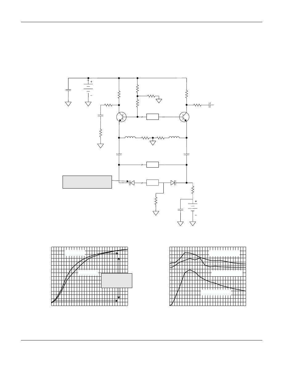
Wideband Balanced VCO Schematic
An even wider tuning range may be achieved with a
balanced VCO configuration. The reason for its wider
tuning performance is that the phase response of this
VCO’s active element is flatter over the range of tuning
compared to a Colpitts VCO. This allows the tank circuit
more control over the oscillation frequency.
The best results are achieved with back-to-back
connected SMV1265 varactors, where there is
820–2120 MHz coverage.
VCO Designs for Wireless Handset and CATV Set-Top Applications
APN1012
V
1
NE68119
V
2
NE68119
T1
16 x 0.4 mm
T2
15 x 0.7 mm
C
1
10
C
2
10
L
1
33 nH
L
2
33 nH
R
1
33
R
2
33
R
3
120
R
4
120
R
5
820
R
7
51
R
8
1 k
R
6
820
R
10
2.4 k
D
1
R
9
1 k
R
11
1000
C
3
100
V
VAR1
V
CC1
5–8 V
C
4
100
C
5
100
R
12
5
0
A
D
2
SMV1265
SMV1265
T3
3 X 0.7 mm
C
6
1000
High C (V) Ratio
Hyperabrupt Varactors
0
5
10
15
20
25
30
Varactor Voltage (V)
Varactor Voltage (V)
0.8
1.0
1.2
1.4
1.6
1.8
2.0
2.2
Frequency (GHz)
Frequency Tuning
0
5
10
15
20
25
30
-8
-6
-4
-2
0
2
4
6
8
Power (dBm)
Power Response
Useful Tuning
Range:
820–2120 MHz
Measured @ 7 V
Simulated @ 7 V
Measured @ 5 V
Measured
Simulations
Figure 9. Wideband Balanced VCO Schematic
Figure 10. Wideband Balanced VCO Performance
10
Alpha Industries, Inc. [781] 935-5150
• Fax [617] 824-4579 • Email sales@alphaind.com • www.alphaind.com
Specifications subject to change without notice. 8/99A
Varactor Fundamentals
Let us consider some fundamental properties of
varactors. A varactor is a specially designed P-N junction
diode, whose capacitance changes significantly in
reverse bias mode. There are three important parameters
characterizing varactors. The first is the capacitance ratio
at two reverse voltages; this value characterizes the tuning
ability of the varactor capacitance and is one of the most
important parameters. The second is the value of
capacitance at a given voltage. The third is the series
resistance of the varactor.
The structure of the basic varactor, called an abrupt
junction varactor, is shown in Figure 11. Generally, it is built
as a P++ - N - N+ structure, using epitaxial N-growth on
the N+ substrate with a constant doping level in the N-
region. The lower doped N-region is the active area where
the electron concentration changes depending on the
reverse voltage applied between the anode and cathode
of the varactor. There are certain limitations on the level
of doping in the N-region, which is usually defined by the
required capacitance ratio of the varactor. Because of this,
the conductance of the N-area is a major contributor to
the varactor’s series resistance. Note that as the reverse
voltage is increased, the series resistance (due to the
N-area) will decrease along with the capacitance.
The hyperabrupt junction varactor has a more
complicated doping profile. Because of much higher
doping on the P++ border, the electron concentration
changes much more abruptly compared to an abrupt
junction. As a result, the capacitance of the hyperabrupt
diode at zero bias is much higher than for the abrupt diode.
Therefore, the capacitance change vs. reverse bias
becomes significantly higher for hyperabrupt diodes. The
trade-off for this better capacitance ratio is increased
series resistance. The reason is that the doping level of
the N-area has been reduced to keep average doping level
over the N-region the same as the abrupt diode level.
There are many ways to bring the series resistance in the
hyperabrupt diode to as low a level as possible. Modern
state-of-the-art hyperabrupt diodes for low noise VCOs
have series resistance almost as low as discrete
ceramic capacitors.
VCO Designs for Wireless Handset and CATV Set-Top Applications
APN1012
P++
Doping
Level
N
Depth from Anode
V
0
V
0
V
1
V
1
V
2
V
2
V
SAT
V
SAT
Electron Concentration
P++
Doping
Level
N+
N
Depth from Anode
Electron Concentration
Abrupt Junction
Hyperabrupt Junction
N+
Figure 11. Varactor Fundamentals
Alpha Industries, Inc. [781] 935-5150
• Fax [617] 824-4579 • Email sales@alphaind.com • www.alphaind.com
11
Specifications subject to change without notice. 8/99A
Varactor Packaging
Most high-volume discrete applications require varactors
in low cost, small surface mount plastic packages. Alpha
Industries provides a large variety of both plastic and
ceramic packages. The recent most advanced miniature
plastic package, SC-79, shown in Figure 12, is as small
as 0402 discrete components.
VCO Designs for Wireless Handset and CATV Set-Top Applications
APN1012
24 mil (0.62 mm)
62 mil (1.58 mm)
SC-79
Figure 12. Varactor Packaging
The coupling coefficient may be derived from the known
(or typical) values of the tuning frequency and varactor
capacitance variation. Note that the total temperature drift
in this case is about 0.5%, as compared to 1% maximum
drift caused by temperature compensated discrete
ceramic capacitors. Even those numbers are extremely
small when compared to the temperature drifts caused by
a VCO transistor.
For the Typical Wireless Case:
f = 1.6 ± -0.04 GHz
Using SMV1235-011 Varactor:
The Total Temperature Drifts
Due to Varactor in the
-40 to +85˚C Becomes:
L
RES
C
RES
C
DIV1
C
DIV2
C
BE
C
CE
C
CB
C
SER2
C
VAR
0.24
8
1.6 GHz
0.08 GHz
2
2
≈
=
x
x
∆C
VAR
=
3.4 pF
pF
C
f
∆f
K
Compare to the Discrete Capacitor!
f
∆f
T
%
54
.
0
≈
12
Alpha Industries, Inc. [781] 935-5150
• Fax [617] 824-4579 • Email sales@alphaind.com • www.alphaind.com
Specifications subject to change without notice. 8/99A
VCO Designs for Wireless Handset and CATV Set-Top Applications
APN1012
Relative Capacitance Change vs.
Temperature
Figure 13 shows typical relative capacitance variations vs.
temperature for different reverse voltages. It indicates a
total capacitance change of 5–6% in the range of -40°C
to +80°C. In comparison, a temperature compensated
ceramic capacitor residual variation bar is shown for a
typical ±100 ppm device. This has a possible total
capacitance change of over 2%. When comparing the
overall effect of temperature on varactors and ceramic
capacitors, the coupling of the devices to the resonator
circuit should be considered.
-4
-3
-2
-1
0
1
2
3
4
5
-40
-20
0
20
40
60
80
Temperature (˚C)
Percentage of Variation (%)
Consider
Varactor
Coupling!!
V
VAR
= -4 V
V
VAR
= -1 V
V
VAR
= -2.5 V
Deviation Range for a Typical
Temperature Compensated
Discrete Ceramic
Multilayer Capacitor
Figure 13. Relative Capacitance Change vs. Temperature for Hyperabrupt Varactors
Figure 14. Varactor Temperature Effect on the Oscillation Frequency
Alpha Industries, Inc. [781] 935-5150
• Fax [617] 824-4579 • Email sales@alphaind.com • www.alphaind.com
13
Specifications subject to change without notice. 8/99A
VCO Designs for Wireless Handset and CATV Set-Top Applications
APN1012
M
+ C
P
V
J
V
VAR
C
GO
C
V
=
1 +
SPICE Model for SMV1142-011
Varactor SPICE Model
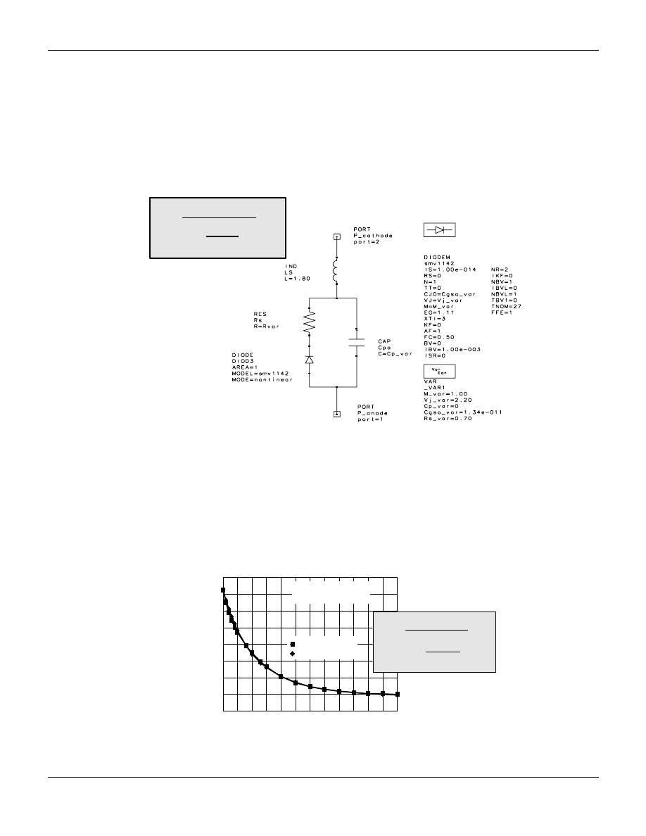
To model a varactor in most commercial simulators, we
recommend the available PN-junction diode SPICE model.
We specify the barrier junction capacitance parameters
C
GO
, V
J
, and M instead of the default parameters. In
addition, we add a value of C
P
, in parallel with the junction
capacitor, which is not the package capacitance. For ideal
abrupt junction varactors, the parameters are constant and
may be defined from physical theory. However, for actual
abrupt or hyperabrupt varactors, these values are not
constant. In these cases, we use the same equation, to
fit its parameters, for the best compliance with measured
capacitance vs. voltage response.
Because of formalization, parameters describing the
junction capacitance of hyperabrupt varactors may be
significantly different from the default values used in the
SPICE simulators for the ideal silicon PN-junction.
For example, typical hyperabrupt varactor SMV1235 was
fitted with M = 4 as opposed to 0.5, which follows silicon
PN diode theory. Note that some SPICE simulators offer
fixed default values of M = 0.5 which can’t be changed.
In this case, a diode model may not be used, however,
direct nonlinear capacitance may be used as defined in
the given formula.
0
2
4
6
8
10
12
Varactor Voltage
0
5
10
15
20
Capacitance (pF)
SMV1235
Approximation
SMV1235
16.13/(1-Vv/8)^4 + 2
8
1+
16.13
4
+ 2
=
V
VAR
C
V
Figure 15. Typical Varactor SPICE Model
Figure 16. C (V) Curve Fitting for Typical Hyperabrupt Varactor
14
Alpha Industries, Inc. [781] 935-5150
• Fax [617] 824-4579 • Email sales@alphaind.com • www.alphaind.com
Specifications subject to change without notice. 8/99A
Super-hyperabrupt Varactor Modeling
To overcome limitations of the “standard” PN-junction
SPICE model for hyperabrupt and super-hyperabrupt
devices, such as the SMV1265, an interleaving technique
is used. In this technique, the entire capacitance reverse
voltage range is broken into several subranges. These
subranges are small enough for the formula to provide
good approximation not only within a given subrange, but
also for certain extensions beyond it. The extension margin
is defined from previously estimated RF signal amplitude.
Such interleaving ensures that the formula would work well
not only in terms of DC bias, but for large-signal RF
analysis as well.
VCO Designs for Wireless Handset and CATV Set-Top Applications
APN1012
M =
pwl (V
VAR
0 2 2.5 2 2.500009 25 6.5 25 6.50009 7.3 11 7.3 11.0009 1.8 40 1.8)
V
J
=
pwl (V
VAR
0 4 2.5 4 2.500009 68 6.5 68 6.50009 14 11 14 11.0009 1.85 40 1.85)
C
P
=
pwl (V
VAR
0 0 2.5 0 2.500009 0 6.5 0 6.50009 0.9 11 0.9 11.0009 0.56 40 0.56)
C
JO
=
pwl (V
VAR
0 22.5 2.5 22.5 2.500009 21 6.5 21 6.50009 20 11 20 11.0009 20 40 20)*10
-12
R
S
=
pwl (V
VAR
0 2.4 3 2.4 4 2.3 5 2.2 6 2 7 1.85 8 1.76 9 1.7 10 1.65 11 1.61 12 1.5 40 1.5)
0
5
10
15
20
25
30
Varactor Voltage
0.1
1.0
10
100
Capacitance (pF)
0
0.2
0.4
0.6
0.8
1.0
Approximation
Measured
SMV1265
Interleaving of Splines
Figure 17. Piece-Wise Curve Fitting for High C (V) Ratio Varactors
Alpha Industries, Inc. [781] 935-5150
• Fax [617] 824-4579 • Email sales@alphaind.com • www.alphaind.com
15
Specifications subject to change without notice. 8/99A
VCO Modeling Concept
For the purpose of modeling and analysis, a VCO design
may be simulated as an amplifier with parallel feedback.
This analysis involves measuring loop gain using a specific
idealized directional coupler called “OSCTEST” in
Libra IV. (For Harmonica users there is an application note
showing how to implement OSCTEST function using
S-parameters file. Refer to your Harmonica vendor for
more information).
VCO Designs for Wireless Handset and CATV Set-Top Applications
APN1012
RL
L
C
C1
C2
I1
I2
V1
V2
Simplified Colpitts VCO
Feedback Model of Colpitts VCO
Amplifier
Tank Circuit
Loop Gain
Observation
Plain
Figure 18. VCO Modeling Concept
16
Alpha Industries, Inc. [781] 935-5150
• Fax [617] 824-4579 • Email sales@alphaind.com • www.alphaind.com
Specifications subject to change without notice. 8/99A
VCO Designs for Wireless Handset and CATV Set-Top Applications
APN1012
The major goal of the large-signal open loop VCO analysis
is to observe the magnitude (defined in dB) and the phase
of the open loop voltage gain Ku, to identify particular
features of the designed VCO.
First, we need to establish the optimum conditions for the
oscillations in a given tuning range. Second, we need to
find out whether there are possibilities for parasitic
oscillations both in the lower and higher frequency ranges.
If there are parasitic oscillations, some preventive
measures should be taken. Third, we need to find ways
to make both Q
L
and the loop power (P
IN
) as high as
possible to facilitate phase noise performance. Finally,
other features of the VCO need to be addressed, among
them load pulling and V
CC
pushing.
1.0
1.5
2.0
2.5
3.0
3.5
Frequency (GHz)
-4
-3
-2
-1
0
1
2
3
4
Mag (Ku) dB
-200
-100
0
100
200
Oscillation
Point
Arg (Ku)
Mag (Ku)
0.5
1.0
1.5
2.0
2.5
Frequency
-250
-200
-150
-100
-50
50
0
100
V
VAR
= 0 V
Transitor X at P
IN
= 10 dBm
Resonator at Different
Varactor Voltages
Parallel Resonance:
When it nears the oscillation
point, tank circuit losses
increase; noise increase and
power decrease follows
Oscillation Happens at the 0 dB Gain
and 0 Loop Phase Shift
V
VAR
= 30 V
Figure 19. Typical Loop Gain Results for the Colpitts VCO
Alpha Industries, Inc. [781] 935-5150
• Fax [617] 824-4579 • Email sales@alphaind.com • www.alphaind.com
17
Specifications subject to change without notice. 8/99A
VCO Designs for Wireless Handset and CATV Set-Top Applications
APN1012
Wideband Colpitts VCO Model
The OSCTEST component interrupts the oscillator
feedback, allowing the designer to analyze the VCO as an
ordinary two-port circuit (amplifier). To observe the loop
response, we define the open loop voltage gain Ku. For
more details, please refer to the VCO application notes
listed in the References section. The varactor model is
defined as a PN-junction diode SPICE model for large
signal harmonic balance analysis. The transistor is
described by the Gumel Poon SPICE model with
parameters provided by the vendor.
Transistor
Subcircuit
Seamless
VCO Loop
Opener
Varactor
Model
Figure 20. Wideband Colpitts VCO Model
18
Alpha Industries, Inc. [781] 935-5150
• Fax [617] 824-4579 • Email sales@alphaind.com • www.alphaind.com
Specifications subject to change without notice. 8/99A
VCO Designs for Wireless Handset and CATV Set-Top Applications
APN1012
Differential VCO Fundamentals
The differential VCO utilizes paired transistors in
common-emitter and common-base configurations. The
phase balance condition for sustaining oscillations
requires significantly lower phase shift in comparison to
a Colpitts design (ideally 0 degrees vs. 180 degrees). This
makes it possible to use a resonator tuned to the exact
resonant frequency. However, the feedback losses may be
higher because the higher resonating currents will cause
increased ohmic losses.
Resonator Works at it’s
Parallel Resonance, Giving
Best Phase Slope Performance
Two Transistors in the
Loop Give Advantage
of Higher Loop Gain
Common-collector -
Common-base Phase
Shift Ideally Is 0
Figure 21. Concept of Differential VCO
Alpha Industries, Inc. [781] 935-5150
• Fax [617] 824-4579 • Email sales@alphaind.com • www.alphaind.com
19
Specifications subject to change without notice. 8/99A
VCO Designs for Wireless Handset and CATV Set-Top Applications
APN1012
Balanced VCO Fundamentals
Fundamental properties of the balanced VCO are more
clearly understood using the simplified circuit diagram
shown in Figure 22. The transistors are in common
collector configuration. This is characterized by high input
impedance, looking from the transmission line and
referenced as L
B
. Capacitor C
BP
simulates the
transmission lines and the grounding effect of the
mounting pads. Coupling current ICPL circulates between
the transistor bases to drive them with a 180° phase shift.
The emitter current I
FB
forms the feedback loop, carrying
an amplified energy surplus that is needed to sustain
resonant current I
RES
and coupling current ICPL through
the emitter-base path. Unlike a Colpitts VCO, this circuit
does not require frequency dependent feedback to match
the internal transistor high frequency phase shifts. When
properly compensated for wideband performance with
inter-base inductor, L
B
, this circuit will be more broadband
than a Colpitts VCO.
L
PAR
L
SER
D
VAR
Re2
Le2
C
BP
C
BP
Re1
Le1
L
B
Rcol
C
BP
C
BP
Rcol
I
CPL
I
FB
I
RES
Low-pass Matching
Serves to Improve
High-frequency
Performance
Collector Currents
are Shifted 180˚
In Phase. That’s
Why We Call It
“Balanced”
Figure 22. Balanced VCO Fundamentals
References
“Varactor SPICE Models for RF VCO Applications.”
Applications Note APN1004, Alpha Industries, Inc., 1998.
“A Colpitts VCO for Wideband (0.95 GHz–2.15 GHz) Set-
Top TV Tuner Applications.” Applications Note APN1006,
Alpha Industries, Inc., 1998.
“A Balanced Wideband VCO for Set-Top TV Tuner
Applications.” Applications Note APN1005, Alpha
Industries, Inc., 1998.
“Switchable Dual-Band 170/420 MHz VCO For Hand-Set
Cellular Applications.” Applications Note APN1007,
Alpha Industries, Inc., 1998.
“A Wideband General Purpose PIN Attenuator.”
Applications Note APN1003, Alpha Industries, Inc., 1999.
“Wideband VCO for Set-Top Applications.” Microwave
Journal, April 1999.
“Circuit Models for Plastic Packaged Microwave Diodes.”
Applications Note APN1001, Alpha Industries, Inc.
“Design with PIN Diodes.” Applications Note APN1002,
Alpha Industries, Inc.
For the availability of the above materials, visit Alpha
Industries Web site at: www.alphaind.com.
Wyszukiwarka
Podobne podstrony:
EARQ Energy Aware Routing for Real Time and Reliable Communication in Wireless Industrial Sensor Net
High Frequency VCO design and schematics
2 grammar and vocabulary for cambridge advanced and proficiency QBWN766O56WP232YJRJWVCMXBEH2RFEASQ2H
A New Hybrid Transmission designed for FWD Sports Utility Vehicles
Flash on English for Mechanics, Electronics and Technical Assistance
06 User Guide for Artlantis Studio and Artlantis Render Export Add ons
BRAUN recipes for your baby and toddler
Chemistry for Environmental Engineering and Science
general settings for user authentication and accounting
Perfect Phrases in Spanish for Household Maintenance and Child Care
A Guide for Counsellors Psychotherapists and Counselling
Check Your Vocabulary for Phrasal Verbs and Idioms
Design For Pcb Emi Emc Compliance
Blade sections for wind turbine and tidal current turbine applications—current status and future cha
116286 PET for Schools Reading and Writing Overviewid 13000
33 437 452 Primary Carbides in Spincast HSS for Hot Rolls and Effect on Oxidation
English for CE EE and water id Nieznany
Homeopathy for Colds, flu and coughs
4 39 48 New Hot Work Steel for High Temp and High Stress Service Conditions
więcej podobnych podstron