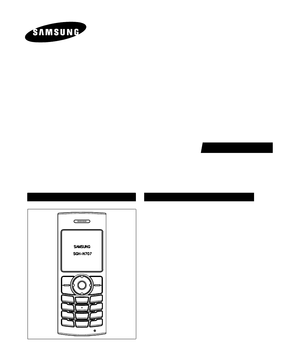
SGH-N707
SERVICE
Manual
GSM TELEPHONE
CONTENTS
1.
Specification
2.
Circuit Description
3.
Exploded Views and Parts List
4.
Electrical Parts List
5.
Block Diagrams
6.
PCB Diagrams
7.
Flow Chart of Troubleshooting
GSM TELEPHONE
ELECTRONICS
Samsung Electronics Co.,Ltd. APRIL. 2004
Printed in Korea.
Code No.: GH68-05461A
BASIC.
ⓒ
This Service Manual is a property of Samsung Electronics Co.,Ltd.
Any unauthorized use of Manual can be punished under applicable
International and/or domestic law.
SAMSUNG Proprietary-Contents may change without notice
1. SGH-N707 Specification
This Document can not be used without Samsung's authorization
1-1
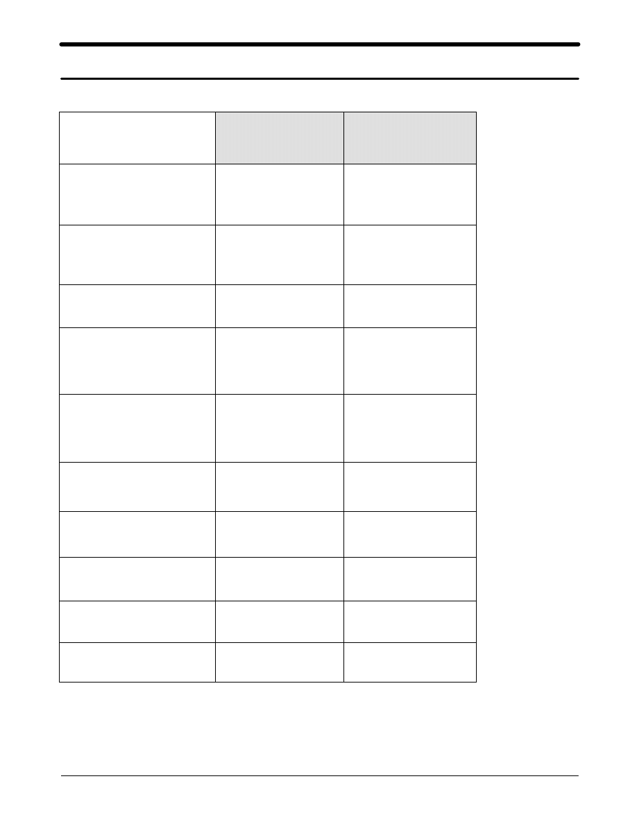
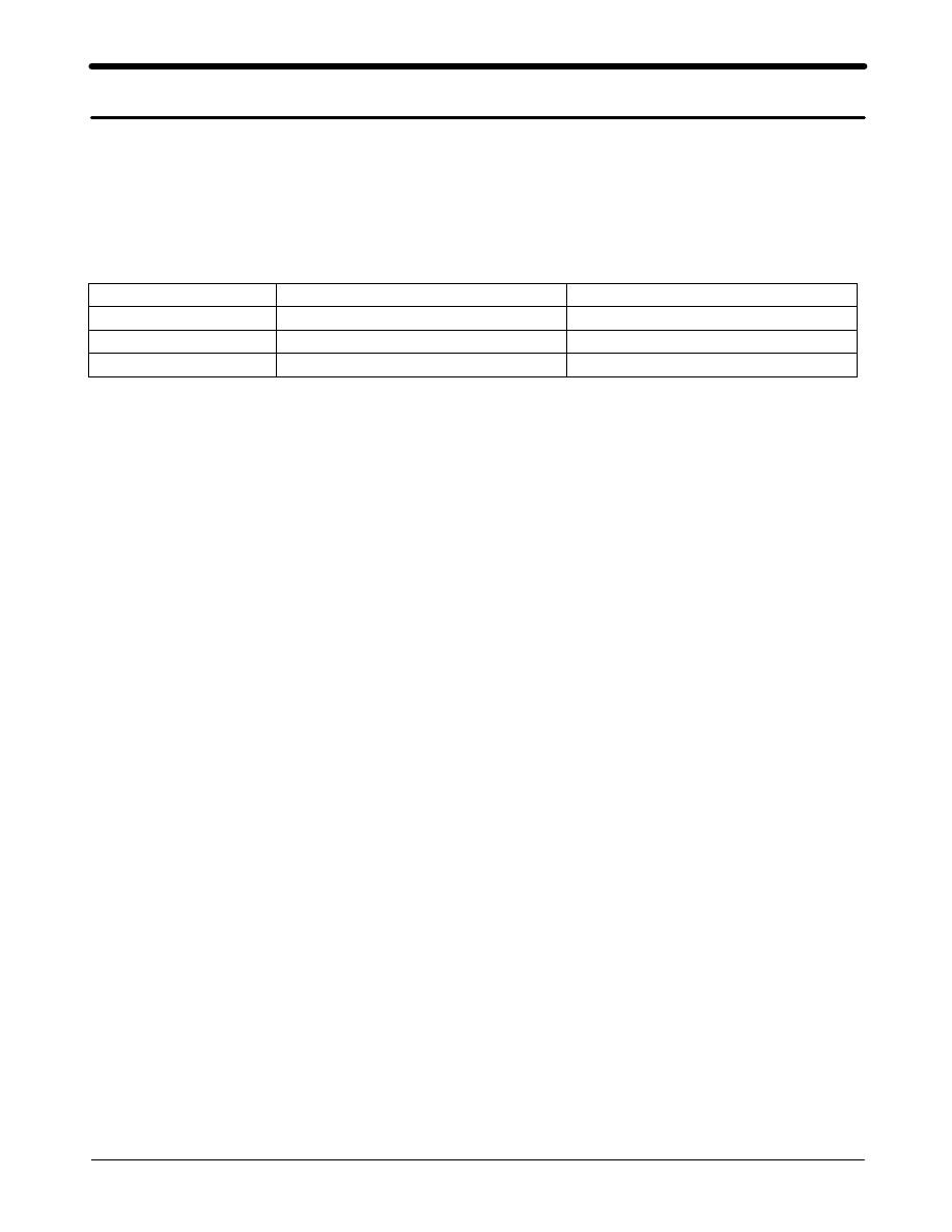
1. GSM General Specification
G S M 8 5 0
P C S 1 9 0 0
F r e q . B a n d [ M H z ]
U p l i n k / D o w n l i n k
8 2 4 ~ 8 4 9
8 6 9 ~ 8 9 4
1 8 5 0 ~ 1 9 1 0
1 9 3 0 ~ 1 9 9 0
A R F C N r a n g e
1 2 8 ~ 2 5 1
5 1 2 ~ 8 1 0
T x / R x s p a c i n g
4 5 M H z
8 0 M H z
M o d . B i t r a t e /
B i t P e r i o d
2 7 0 . 8 3 3 k b p s
3 . 6 9 2 u s
2 7 0 . 8 3 3 k b p s
3 . 6 9 2 u s
T i m e S l o t P e r i o d / F r a me
P e r i o d
5 7 6 . 9 u s
4 . 6 1 5 m s
5 7 6 . 9 u s
4 . 6 1 5 ms
M o d u l a t i o n
0 . 3 G M S K
0 . 3 G M S K
M S P o w e r
3 3 d B m ~ 5 d B m
3 0 d B m~ 0 d B m
P o w e r C l a s s
5 p c l ~ 1 9 p c l
0pcl ~ 15pcl
S e n s i t i v i t y
- 1 0 2 d B m
- 1 0 2 d B m
T D M A M u x
8
8
SAMSUNG Proprietary-Contents may change without notice
This Document can not be used without Samsung's authorization
Specification
1-2
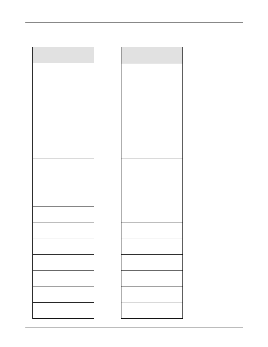
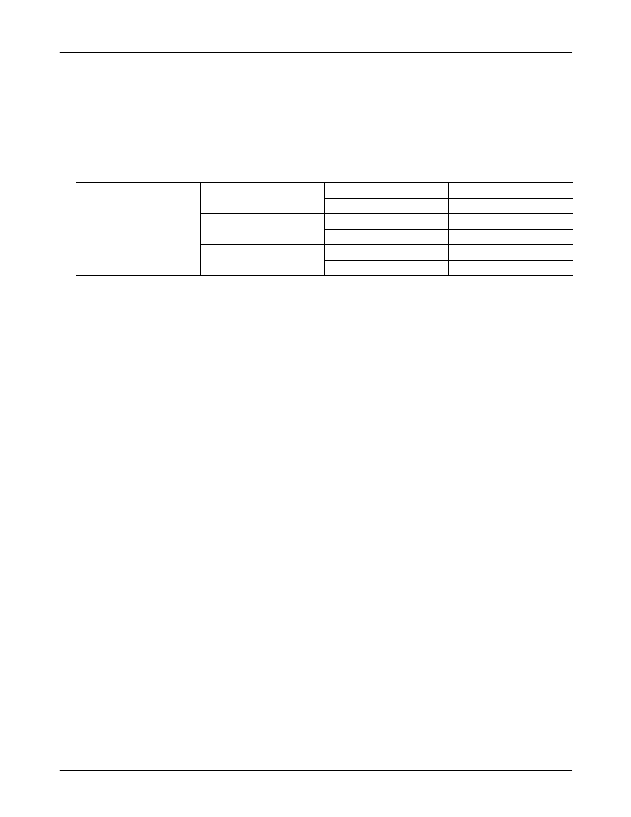
2. GSM TX power class
TX Power
control level
GSM850
5
33±2 dBm
6
31±2 dBm
7
29±2 dBm
8
27±2 dBm
9
25±2 dBm
10
23±2 dBm
11
21±2 dBm
12
19±2 dBm
13
17±2 dBm
14
15±2 dBm
15
13±2 dBm
16
11±3 dBm
17
9±3dBm
18
7±3 dBm
19
5±3 dBm
TX Power
control level
PCS1900
0
30±2 dBm
1
28±3 dBm
2
26±3 dBm
3
24±3 dBm
4
22±3 dBm
5
20±3 dBm
6
18±3 dBm
7
16±3 dBm
8
14±3 dBm
9
12±4 dBm
10
10±4 dBm
11
8±4dBm
12
6±4 dBm
13
4±4 dBm
14
2±5 dBm
15
0±5 dBm
SAMSUNG Proprietary-Contents may change without notice
2. SGH-N707 Circuit Description
This Document can not be used without Samsung's authorization
2-1
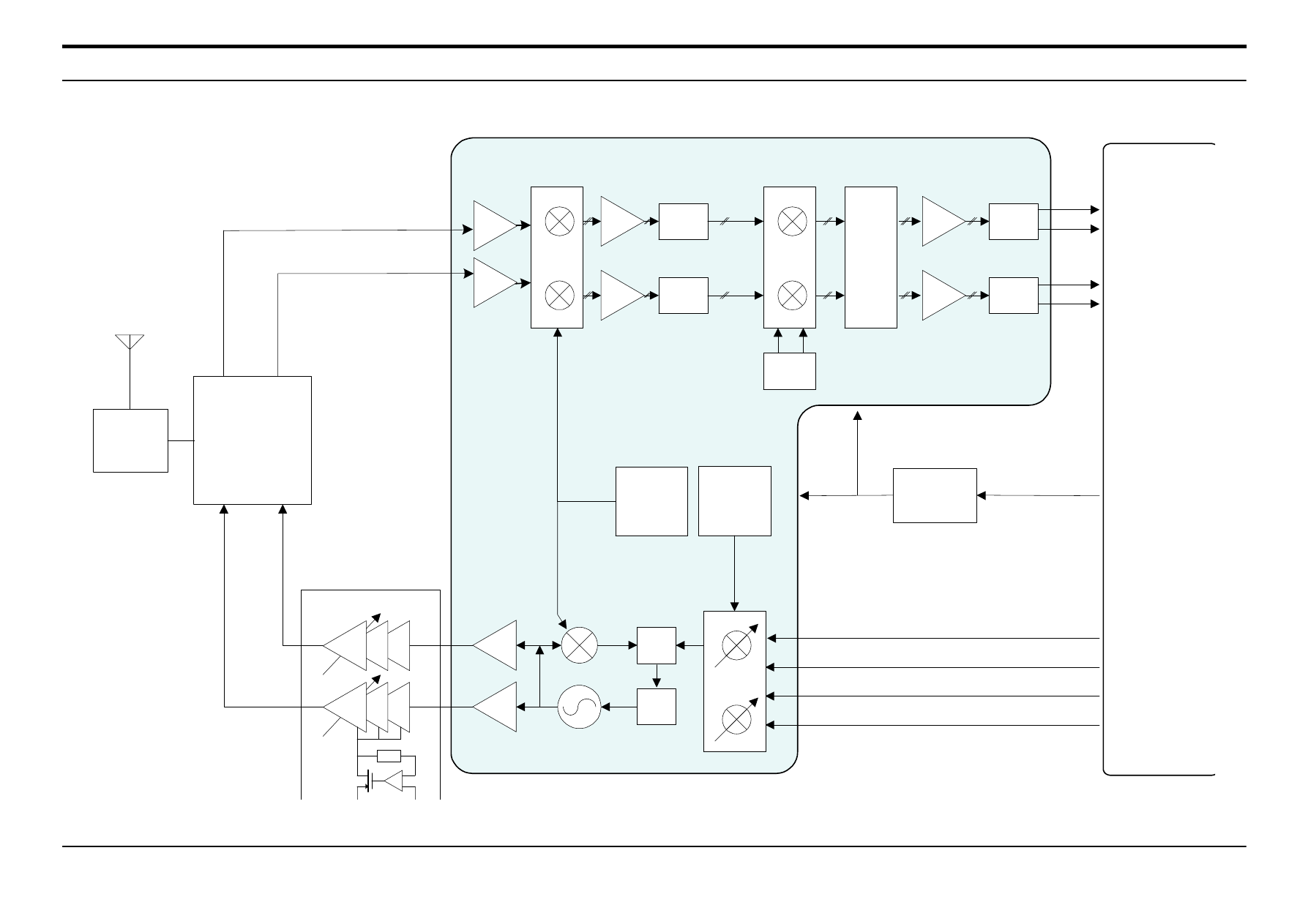
1. SGH-N707 RF Circuit Description
1) RX PART
1. FEM(U402(SWITCHPLEXER+FILTER)) → Switching Tx, Rx path for GSM850, and PCS1900 by logic controlling.
2. FEM Control Logic (U402) → Truth Table
VC1
VC2
DCS / PCS Tx Mode
L
H
GSM Tx Mode
H
L
GSM / PCS Rx Mode
L
L
3. FILTER
To convert Electromagnetic Field Wave to Acoustic Wave and then pass the specific frequency band.
- GSM FILTER (U402(SWITCHPLEXER+FILTER)) → For filtering the frequency band between 869 ~ 894 MHz
- PCS FILTER(U402(SWITCHPLEXER+FILTER)) → For filtering the frequency band 1930 and 1990 MHz.
4. VC-TCXO (OSC401)
To generate the 13MHz reference clock to drive the logic and RF.
After additional process, the reference clock applies to the U101 Rx IQ demodulator and Tx IQ modulator.
The oscillator for RX IQ demodulator and Tx modulator are controlled by serial data to select channel and use fast lock
mode for GPRS high class operation.
5. SI 4205 (U404)
This chip integrates two differential-input LNAs.
The GSM input supports the GSM850, PCS input supports the DCS1900. The LNA inputs are matched to the 200 ohm
differential output SAW filters through eternal LC matching network.
Image-reject mixer downconverts the RF signal to a 100 KHz intermediate frequency(IF) with the RFLO from frequency
synthesizer. The RFLO frequency is between 1737.8 ~ 1989.9 MHz.
The Mixer output is amplified with an analog programmable gain amplifier(PGA), which is controlled by AGAIN.
The quadrature IF signal is digitized with high resolution A/D converts (ADC).
Also, this chip down-converts the ADC output to baseband with a digital 100 KHz quadrature LO signal. Digital
decimation and IIR filters perform channel selection to remove blocking and reference interface signals.
After channel selection, the digital output is scaled with a digital PGA, which is controlled with the DGAIN. DACs drive
a differential analog signal onto the RXIP, RXIN, RXQP, RXQN pins to interface to standard analog-input baseband IC.
SAMSUNG Proprietary-Contents may change without notice
This Document can not be used without Samsung's authorization
Circuit Description
2-2
2) TX PART
Baseband IQ signal fed into offset PLL, this function is included inside of U404 chip.
SI4205 chip generates modulator signal which power level is about 1.5dBm and fed into Power Amplifier(U403).
The PA output power and power ramping are well controlled by Auto Power Control circuit. We use offset PLL below
Modulation Spectrum
200kHz offset
30 kHz bandwidth
GSM
-35dBc
PCS
-35dBc
400kHz offset
30 kHz bandwidth
GSM
-66dBc
PCS
-65dBc
600kHz ~ 1.8MHz offset
30 kHz bandwidth
GSM
-75dBc
PCS
-68dBc
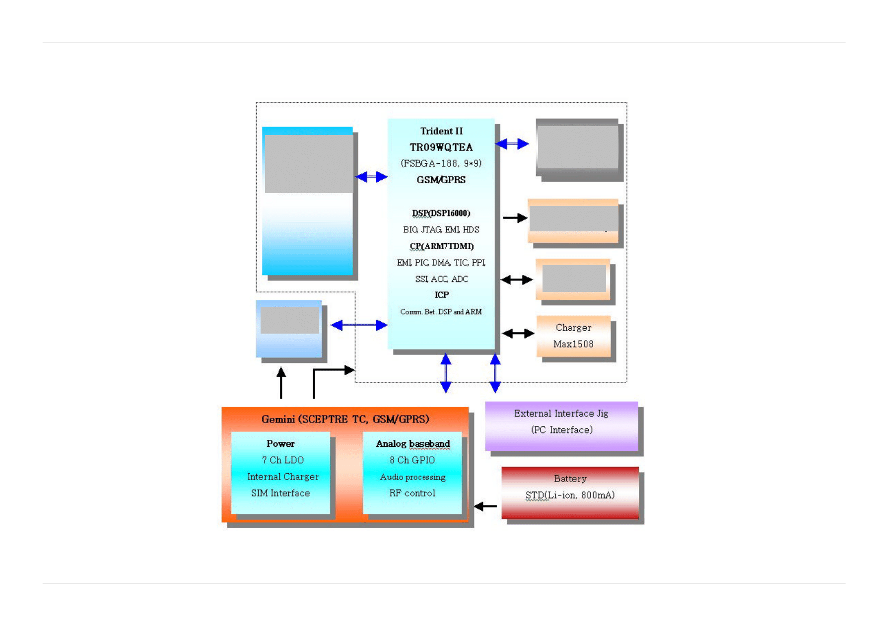
2. Baseband Circuit description of SGH-N707
1) CSP2200B1
1. Power Management
Seven low-dropout regulators designed specifically for GSM applications power the terminal and help ensure optimal
system performance and long battery life. A programmable LDO provides support for 1.8V, 3.0V SIMs, while a
self-resetting, electronically fused switch supplies power to external accessories. Ancillary support functions, such as two
LED drivers and two call-alert drivers, aid in reducing both board area and system complexity. A four-wire serial interface
unit(SIU) provides access to control and configuration registers. This interface gives a microprocessor full control of the
CSP2200B1 and enables system designers to maximize both standby and talk times. Error reporting is provided via an
interrupt signal and status register. Supervisory functions. including a reset generator, an input voltage monitor, and a
thermal monitor, support reliable system design. These functions work together to ensure proper system behavior during
start-up or in the event of a fault condition(low microprocessor voltage, insufficient battery energy, or excessive die
temperature).
2. Battery Charge Management
A battery charge management block, incorporating an internal PMOS switch, and an 8-bit ADC, provides fast, efficient
charging of single-cell Li-Ion battery. Used in conjunction with a current-limited voltage source, this block safely
conditions near-dead cells and provides the option of having fast-charge and top-off controlled internally or by the system's
microprocessor.
3. Backlight LED Driver
The backlight LED driver is a low-side, programmable current source designed to control the brightness of the keyboard
illumination.
LED1_DRV is controlled via LED1_[0:2] and can be programmed to sink from 15mA to 60mA in 7.5mA
steps. LED2_DRV is controlled via LED2_[0:2] and can be programmed to sink from 5mA to 40mA in 5mA steps.

SAMSUNG Proprietary-Contents may change without notice
Circuit Description
This Document can not be used without Samsung's authorization
2-3
Both LED drivers are capable of sinking their maximum output current at a worst-case maximum output voltage of 0.6V.
For efficient use, the LEDs is connected between the battery and the LED_DRV output.
4. Vibrator Motor Driver
The vibrator motor driver is a independent voltage regulator to drive a small dc motor that silently alerts the user of an
incoming call. The driver is a 3.0V constant source while sinking up to 180mA and controlled by enable signal of main
chip. For efficient use and safety, the vibrator motor should be connected between the regulator output and the ground.
2) LCD
LCD is consisted of main LCD(B/W STN LCD). Chip select signals of EMI part in the trident, LCD_CS, can enable
main LCD. VDD_EL signal enables
EL of main LCD. In sleep mode,
EL are turned off.
These two signals are from IO part of the DSP in the trident. RST signal from CSP2200B1 initiates the initial process of
the LCD.
16-bit data lines(D(0)~D(15)) transfers data and commands to LCD . Data and commands use A(2) signal. If this signal is
high, Inputs to LCD are commands. If it is low, Inputs to LCD are data.
The signals which inform the input or output state to LCD, are required. But this system is not necessary for read enable
signal. CP_WEN signal is only used to write data or commands to LCD.
Power signal for operating LCD driver is VCCD.
3) JTAG Connector
Trident has two JTAG ports which are for ARM core and DSP core(DSP16000). So this system has two port connector
for these ports. Pins' initials for ARM core are 'CP_' and pins' initials for DSP core are 'DSP_'.
CP_TDI and DSP_TDI signal are used for input of data. CP_TDO and DSP_TDO signals are used for the output of the
data. CP_TCK and DSP_TCK signals are used for clock because JTAG communication is a synchronous. CP_TMS and
DSP_TMS signals are test mode signals. The difference between these is the RESET_INT signal which is for ARM core
RESET.
4) Keypad
This is consisted of key interface pins in the trident, KEY_ROW[0~4] and KEY_COL[0~4]. These signals compose the
matrix. Result of matrix informs the key status to key interface in the trident. Some pins are connected to varistor for
ESD protection. And power on/off key is seperated from the matrix.
So power on/off signal is connected with CSP2200 to enable CSP2200.

SAMSUNG Proprietary-Contents may change without notice
This Document can not be used without Samsung's authorization
Circuit Description
2-4
5) IF connetor
It is 18-pin connector, and separated into two parts. One is a power supply part for main system. And the other is
designed to use SDS, DEBUG, DLC-DETECT, JIG_ON, TA, VF, and GND. They connected to power supply IC,
microprocessor and signal processor IC.
6) Audio
AOUTAP, AOUTAN from CSP2200 is connected to the speaker via analog switch.
MICIN and MICOUT are connected
to the main MIC.
YMU759 is a LSI for portable telephone that is capable of playing high quality music by utilizing FM synthesizer and
ADPCM decorder that are included in this device.
As a synthesis, YMU759 is equipped 16 voices with different tones. Since the device is capable of simultaneously
generating up to synchronous with the play of the FM synthesizer, various sampled voices can be used as sound effects.
Since the play data of YMU759 are interpreted at anytime through FIFO, the length of the data(playing period) is not
limited, so the device can flexibly support application such as incoming call melody music distribution service. The
hardware sequencer built in this device allows playing of the complex music without giving excessive load to the CPU of
the portable telephones. Moreover, the registers of the FM synthesizer can be operated directly for real time sound
generation, allowing, for example, utilization of various sound effects when using the game software installed in the
portable telephone.
YMU759 includes a speaker amplifier with high ripple removal rate whose maximum output is 550mW (SPVDD=3.6V).
The device is also equipped with conventional function including a vibartor and a circuit for controlling LEDs synchornous
with music.
7) Memory
This system uses AMD's memory,
S71JL064HA0BAW110
.
It is consisted of 64M bits flash memory and 16M bits PSRAM. It has 16 bit data line, D[0~15] which is connected to
trident, LCD or CSP2200. It has 22 bit address lines, A[0~21]. They are also connected. CP_CSROMEN signal, chip
select signal in the trident, enable flash memories. They use 2.8 volt supply voltage, VCCD.
During wrting process, CP_WEN is low and it enables writing process to flash memory and PSRAM. During reading
process, CP_OEN is low and it output information which is located at the address from the trident in the flash memory or
PSRAM to data lines. Each chip select signals in the trident select flash memory or PSRAM. Reading or writing
procedure is processed after CP_WEN or CP_OEN is enabled. Memories use RST. A[0] signal enables lower byte of
PSRAM and UPPER_BYTE signal enables higher byte of PSRAM.

SAMSUNG Proprietary-Contents may change without notice
Circuit Description
This Document can not be used without Samsung's authorization
2-5
8) Trident
Trident is consisted of ARM core and DSP core. It has 20K*16bits RAM 144K*16bits ROM in the DSP. It has
4K*32bits ROM and 2K*32bits RAM in the ARM core. DSP is consisted of timer, one bit input/output unit(BIO), JTAG,
EMI and HDS(Hardware Development System). ARM core is consisted of EMI, PIC(Programmable Interrupt Controller),
reset/power/clock unit, DMA controller, TIC(Test Interface Controller), peripheral bridge, PPI, SSI(Synchronous Serial
Interface), ACCs(Asynchronous communications controllers), timer, ADC, RTC(Real-Time Clock) and keyboard interface.
DSP_AB[0~8], address lines of DSP core and DSP_DB[0~15], data lines of DSP core are connected to CSP2200. A[0~20],
address lines of ARM core and D[0~15], data lines of ARM core are connected to memory, LCD and YMU762.
ICP(Interprocessor Communication Port) controls the communication between ARM core and DSP core.
CSROMEN, CSRAMEN and CS1N to CS4N in the ARM core are connected to each memory. WEN and OEN control the
process of memory. External IRQ(Interrupt ReQuest) signals from each units, such as, YMU, Ear-jack, Ear-mic and
CSP1093, need the compatible process.
Some PPI pins has many special functions. CP_KB[0~9] receive the status from key FPCB and are used for the
communications using data link cable(DEBUG_DTR/RTS/TXD/RXD/CTS/DSR).
And UP_CS/SCLK/SDI, control signals for CSP2200 are outputted through PPI pins. It has signal port for
charging(CHG_DET), SIM_RESET and FLIP_SNS with which we knows open.closed status of folder. It has JTAG control
pins(TDI/TDO/TCK) for ARM core and DSP core. It recieves 13MHz clock in CKI pin from external TCXO and receives
32.768KHz clock from X1RTC. ADC(Analog to Digital Convertor) part receives the status of temperature, battery type and
battery voltage. And control signals(DSP_INT, DSP_IO and DSP_RWN) for DSP core are used. It enables main LCD with
DSP IP pins.
9) X-TAL(13MHz)
This system uses the 13MHz TCXO. AFC control signal form CSP1093 controls frequency from 13MHz x-tal.
. This
clock is fed to CSP1093,Trident,YMU759 and Silab solution.
SAMSUNG Proprietary-Contents may change without notice
3. SGH-N707 Exploded View and its Parts list
3-1
This Document can not be used without Samsung's authorization
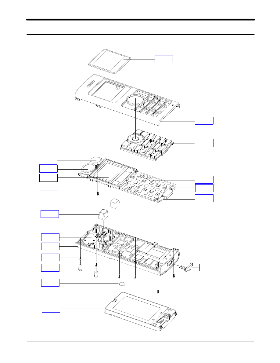
1. Cellular phone Exploded View-1
QRE01
QAN01
QMW02
QFR01
QKP01
QMO02
QSP01
QLC41
QMI01
QME01
QMP01
QIF01
QCR05
QAN05
QCR04
QRE02
QRF01
QBA21
SAMSUNG Proprietary-Contents may change without notice
Exploded view and its Part list
3-2
This Document can not be used without Samsung's authorization
2. Cellular phone Parts list
Location
NO.
Description
SEC CODE
Remark
QMW02
PMO-MAIN WINDOW
GH72-13316A
QFR01
MEC-FRONT COVER
GH75-04537A
QIF01
PMO-IF COVER
GH72-16745A
QKP01
MEC-KEYPAD ASSY
GH75-04539A
QSP01
SPEAKER
3001-001576
QMO02
MOTOR
3101-001328
QMP01
MIAN PBA
GH92-01773A
QLC41
LCD
GH07-00548A
QME01
UNIT METAL DOME
GH59-01456A
QMI01
MICROPHONE ASSY
GH30-00125A
QCR05
SCREW
6001-001478
QAN05
MEC-INTENA RUBBER
GH75-05620A
QRE01
REAR COVER
GH75-04538A
QCR04
SCREW-MACHINE
6001-001479
QRE02
PMO-REAR BUMPER
GH72-16829A
QRF01
MPR-R/F COVER
GH74-08243A
QBA21
BATTERY-820MAH
GH43-01358A
QAN01
ANTENNA
GH42-00429A
SAMSUNG Proprietary-Contents may change without notice
Exploded view and its Part list
3-2
This Document can not be used without Samsung's authorization
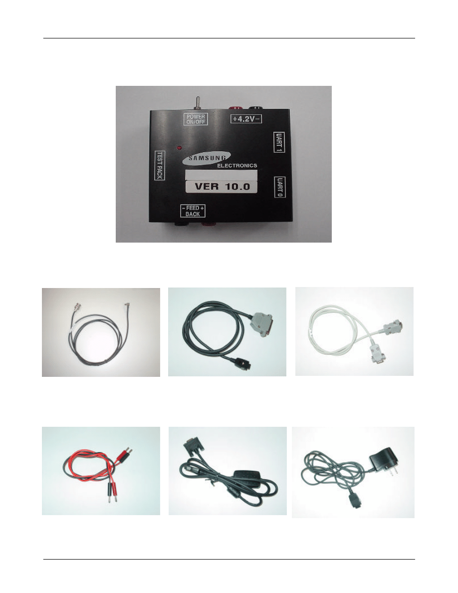
3. Test Jig (GH80-00865A)
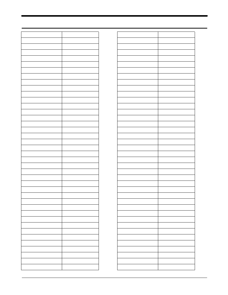
3-1. RF Test Cable
(GH39-00182A)
3-2. Test Cable
(GH39-00127A)
3-3. Serial Cable
3-4. Power Supply Cable
3-5. DATA CABLE
(GH39-00143B)
3-6. TA
(GH44-00284A)
SAMSUNG Proprietary-Contents may change without notice
4. SGH-N707 MAIN Electrical Parts List
4-1
This Document can not be used without Samsung's authorization
SEC CODE
Design LOC
0403-001387
ZD629
0403-001427
ZD628
0403-001511
ZD301
0404-001172
D501
0406-001150
ZD501
0406-001150
ZD502
0501-000481
Q301
0504-001113
Q102
0601-001094
LED601
0601-001094
LED602
0601-001094
LED605
0601-001094
LED606
0601-001094
LED607
0601-001094
LED608
0601-001094
LED631
0601-001094
LED632
0601-001094
LED633
0601-001094
LED634
0601-001094
LED635
0601-001094
LED636
0601-001956
LED610
0801-000796
U102
1001-001261
U501
1003-001395
U302
1109-001309
U202
1201-002177
U403
1203-001917
U601
1203-003109
U107
1203-003304
U101
1204-001811
U502
1205-002433
U404
1209-001219
U203
1405-001082
ZD601
1405-001082
ZD602
1405-001082
ZD603
1405-001082
ZD604
1405-001082
ZD605
1405-001082
ZD606
1405-001082
ZD607
SEC CODE
Design LOC
1405-001082
ZD608
1405-001082
ZD609
1405-001082
ZD610
1405-001082
ZD611
1405-001082
ZD612
1405-001082
ZD613
1405-001082
ZD614
1405-001082
ZD615
1405-001082
ZD616
1405-001082
ZD617
1405-001082
ZD618
1405-001082
ZD619
1405-001082
ZD620
1405-001082
ZD621
1405-001082
ZD622
1405-001082
ZD623
1405-001082
ZD624
2007-000138
R103
2007-000138
R113
2007-000138
R424
2007-000140
R515
2007-000140
R516
2007-000140
R617
2007-000140
R618
2007-000140
R619
2007-000140
R620
2007-000140
R621
2007-000140
R622
2007-000140
R623
2007-000140
R624
2007-000140
R625
2007-000140
R627
2007-000140
R628
2007-000140
R629
2007-000141
R420
2007-000148
R109
2007-000148
R110
2007-000148
R202
2007-000148
R214

SAMSUNG Proprietary-Contents may change without notice
Electrical Parts List
4-2
This Document can not be used without Samsung's authorization
SEC CODE
Design LOC
2007-000148
R423
2007-000148
R510
2007-000148
R512
2007-000157
R207
2007-000157
R609
2007-000157
R610
2007-000162
R111
2007-000162
R112
2007-000162
R114
2007-000162
R201
2007-000162
R206
2007-000162
R501
2007-000162
R511
2007-000162
R513
2007-000164
R504
2007-000171
R102
2007-000171
R104
2007-000171
R105
2007-000171
R106
2007-000171
R108
2007-000171
R210
2007-000171
R213
2007-000171
R302
2007-000171
R425
2007-000171
R426
2007-000171
R509
2007-000171
R518
2007-000171
R519
2007-000171
R521
2007-000690
R301
2007-000775
R505
2007-000775
R506
2007-001119
R517
2007-001217
R601
2007-001217
R602
2007-001217
R605
2007-001217
R606
2007-001217
R607
2007-001217
R608
SEC CODE
Design LOC
2007-001217
R631
2007-001217
R632
2007-001217
R633
2007-001217
R634
2007-001217
R635
2007-001217
R636
2007-001292
R502
2007-001292
R503
2007-001319
R101
2007-001325
R507
2007-002797
R421
2007-003001
R422
2007-003025
R630
2007-007100
R205
2007-007138
R402
2007-007142
R208
2007-007308
R211
2007-007308
R212
2007-008117
R107
2203-000189
C310
2203-000189
C311
2203-000189
C312
2203-000189
C313
2203-000189
C314
2203-000233
C110
2203-000233
C401
2203-000233
C402
2203-000233
C423
2203-000233
C429
2203-000233
C430
2203-000233
C431
2203-000233
C440
2203-000233
C502
2203-000233
C503
2203-000233
C505
2203-000233
C508
2203-000254
C201
2203-000254
C202
2203-000254
C203
SAMSUNG Proprietary-Contents may change without notice
Electrical Parts List
4-3
This Document can not be used without Samsung's authorization
SEC CODE
Design LOC
2203-000254
C204
2203-000254
C205
2203-000254
C206
2203-000254
C207
2203-000254
C208
2203-000254
C212
2203-000254
C418
2203-000254
C419
2203-000254
C438
2203-000254
C441
2203-000254
C442
2203-000254
C443
2203-000254
C449
2203-000278
C530
2203-000425
C439
2203-000438
C512
2203-000628
C220
2203-000628
C221
2203-000628
C407
2203-000628
C410
2203-000628
C435
2203-000654
C504
2203-000679
C211
2203-000812
C107
2203-000812
C108
2203-000812
C109
2203-000812
C436
2203-000885
C303
2203-000995
C414
2203-000995
C434
2203-001072
C101
2203-001072
C102
2203-001072
C114
2203-001072
C215
2203-001072
C216
2203-001405
C507
2203-001598
C111
2203-001598
C112
2203-001598
C116
SEC CODE
Design LOC
2203-001652
C113
2203-005061
C103
2203-005061
C106
2203-005061
C117
2203-005061
C119
2203-005061
C124
2203-005061
C213
2203-005061
C214
2203-005061
C217
2203-005061
C218
2203-005061
C222
2203-005061
C223
2203-005061
C422
2203-005061
C506
2203-005061
C510
2203-005061
C513
2203-005061
C532
2203-005065
C302
2203-005065
C305
2203-005065
C306
2203-005065
C307
2203-005065
C523
2203-005065
C609
2203-005065
C610
2203-005281
C411
2203-005281
C413
2203-005288
C408
2203-005288
C409
2203-005446
C450
2203-005480
C219
2203-005482
C304
2203-005482
C501
2203-005496
C118
2203-005496
C209
2203-005496
C210
2203-005509
C515
2203-005509
C521
2203-006093
C115
2203-006093
C120
SAMSUNG Proprietary-Contents may change without notice
Electrical Parts List
4-4
This Document can not be used without Samsung's authorization
SEC CODE
Design LOC
2203-006093
C315
2203-006257
C121
2203-006257
C122
2203-006324
C104
2203-006324
C105
2404-001086
C511
2404-001239
C602
2404-001268
C123
2404-001281
C417
2404-001281
C433
2404-001305
C529
2404-001339
C509
2404-001348
C406
2703-002102
L401
2703-002201
L402
2703-002201
L405
2703-002624
L301
2703-002665
L403
2801-003747
OSC201
2809-001264
OSC401
2909-001236
U402
3705-001287
U401
3709-001335
CN101
3710-002017
CN601
4302-001130
BAT101
GH09-00028A
U201
SAMSUNG Proprietary-Contents may change without notice
This Document can not be used without Samsung's authorization
5. SGH-N707 Block Diagrams
5-1
1. RF Solution Block Diagram
GSM RX (869~984 MHz)
LN A
PG A
PG A
ADC
ADC
VCT CXO
(OSC401)
GSM TX
(824 ~ 849 MH z)
PCS TX
(1850 ~ 1910 MHz)
Dua l PA M
(U403)
Fr ont
En d
Mod ule
(U402)
RF
Connector
(U401)
Si 42 05
(U404)
RF
PLL
IF
PLL
PD
LPF
Mi x e r
Channel
Fi
lt
er
PG A
PG A
DAC
DAC
10 0
kH z
CS P
22 00 B1
(U101)
Bryc e Park
I
Q
I
Q
SDATA
SCLK
SENB
PDNB
LN A
PCS RX ( 1960 MHz )
SAMSUNG Proprietary-Contents may change without notice
Block Diagrams
This Document can not be used without Samsung's authorization
5-2
2. Base Band Solution Block Diagram
MEMORY
NOR
64Mb Flash
+16Mb PSRAM
Keypad Without
Volume Side key
Melody-16
YMU759
RF I/F
(Si4205)
STN-LCD
128 x 64
B/W(WINTEK)
SAMSUNG Proprietary-Contents may change without notice
This Document can not be used without Samsung's authorization
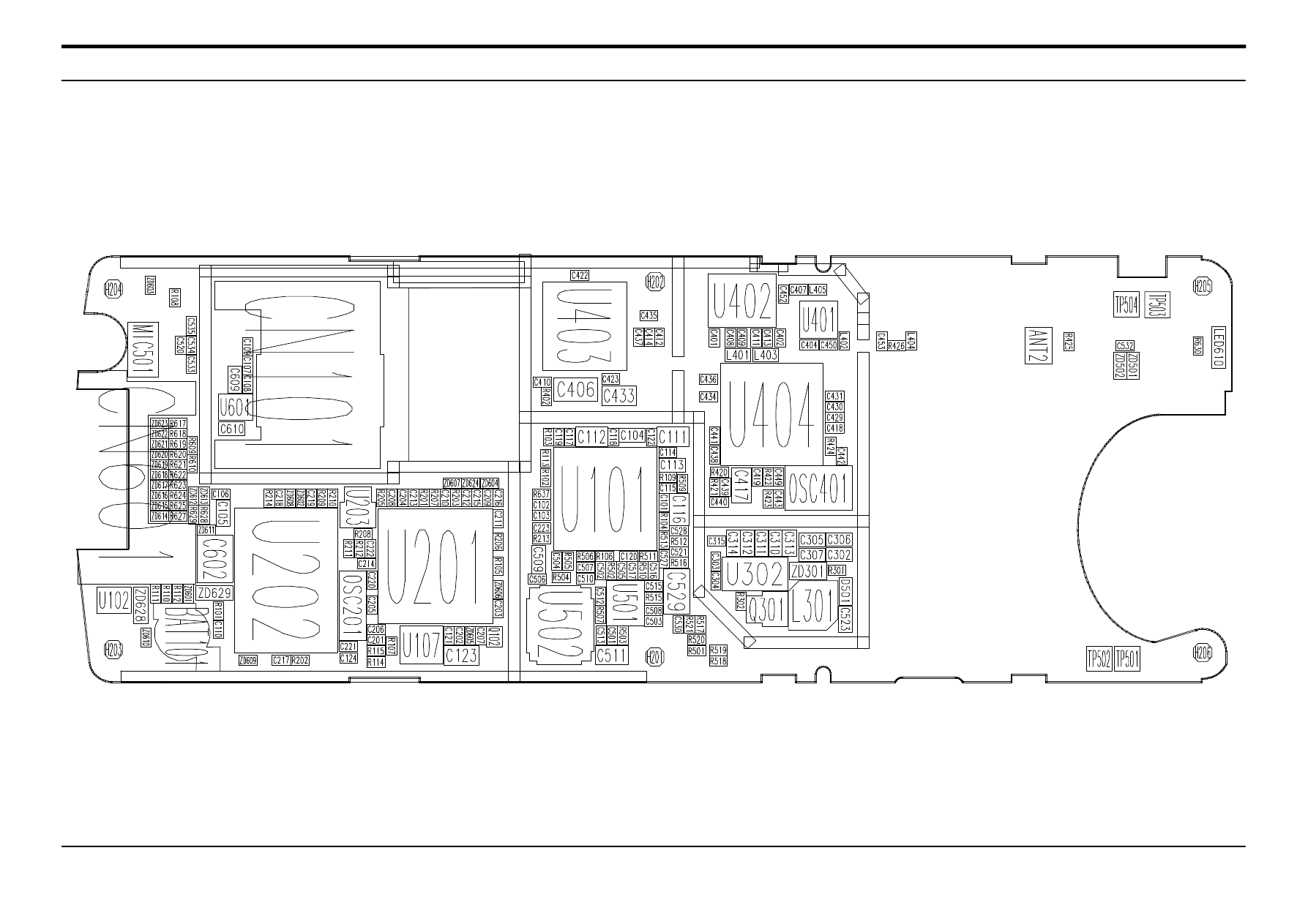
6. SGH-N707 PCB Diagrams
6-1
1. Main PCB Top Diagram
SAMSUNG Proprietary-Contents may change without notice
PCB Diagrams
6-2
This Document can not be used without Samsung's authorization
2. Main PCB Bottom Diagram
SAMSUNG Proprietary-Contents may change without notice
7. SGH-N707 Flow Chart of Troubleshooting
This Document can not be used without Samsung's authorization
7-1
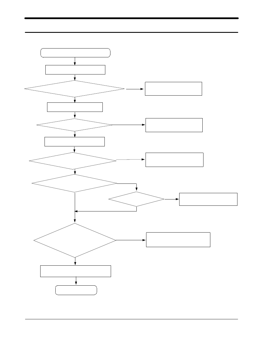
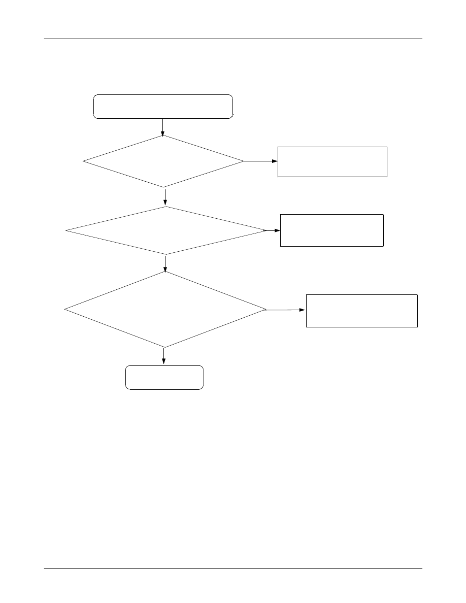
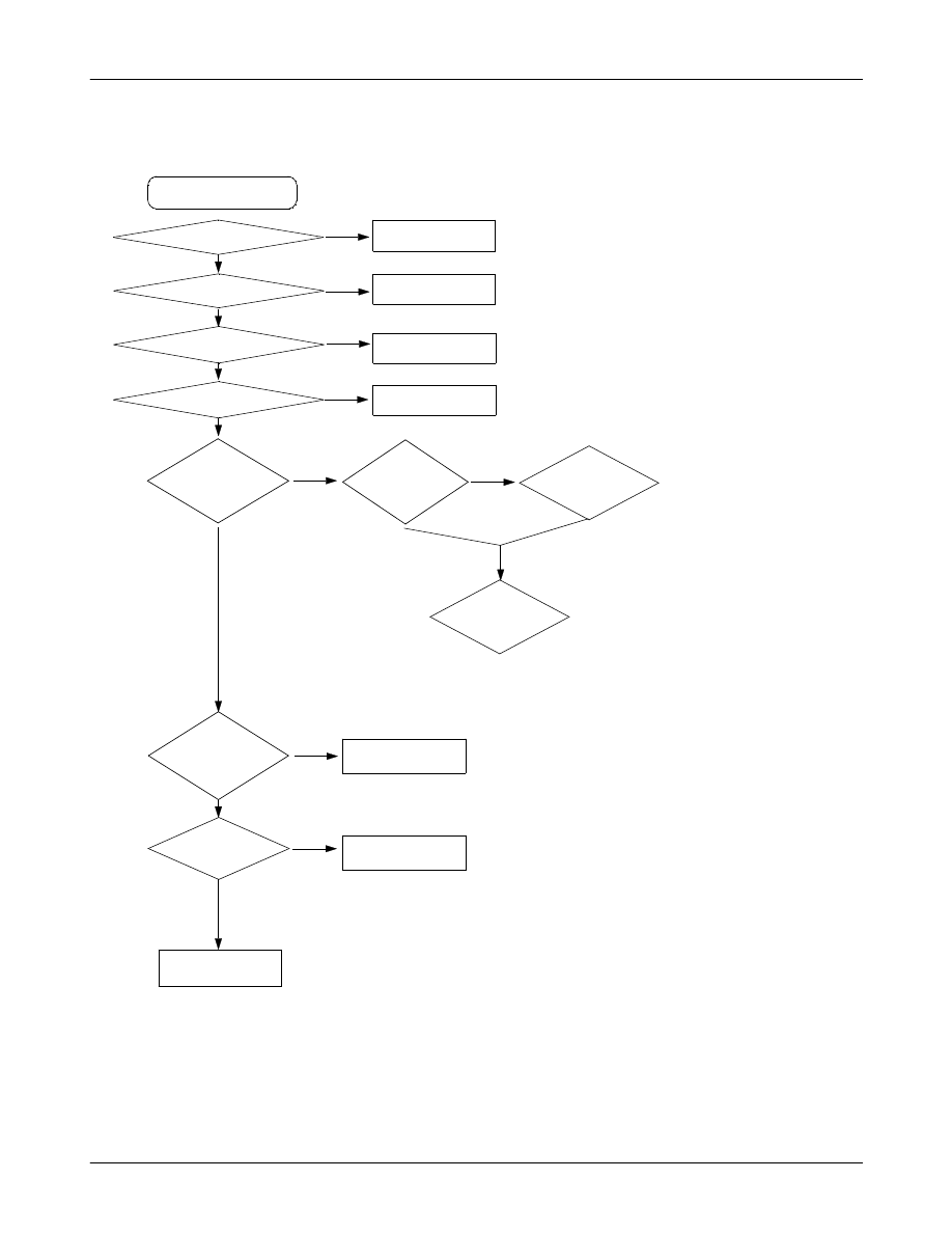
1. Power On
Current consumption
>=100mA
The set is not ' Power On '
Voltage >= 3.3V
Download again
Charge the Battery
pin#J12 of U101 >= 2.8V
Check U101 and C112
pin#A13 of U101 = 2.8V
Check U101 and C115
Check the clock signal
at pin#R6
Freq = 13MHz
Check the clock generation circuit
(related to OSC401)
END
No
Yes
Yes
Yes
Yes
Yes
No
No
No
No
pin#G11 = 1.8V
No
Yes
Check the +VBATT Voltage
Check the pin of U101
Check the initial operation
Check the current consumption
SAMSUNG Proprietary-Contents may change without notice
This Document can not be used without Samsung's authorization
Flow Chart of Troubleshooting
7-2
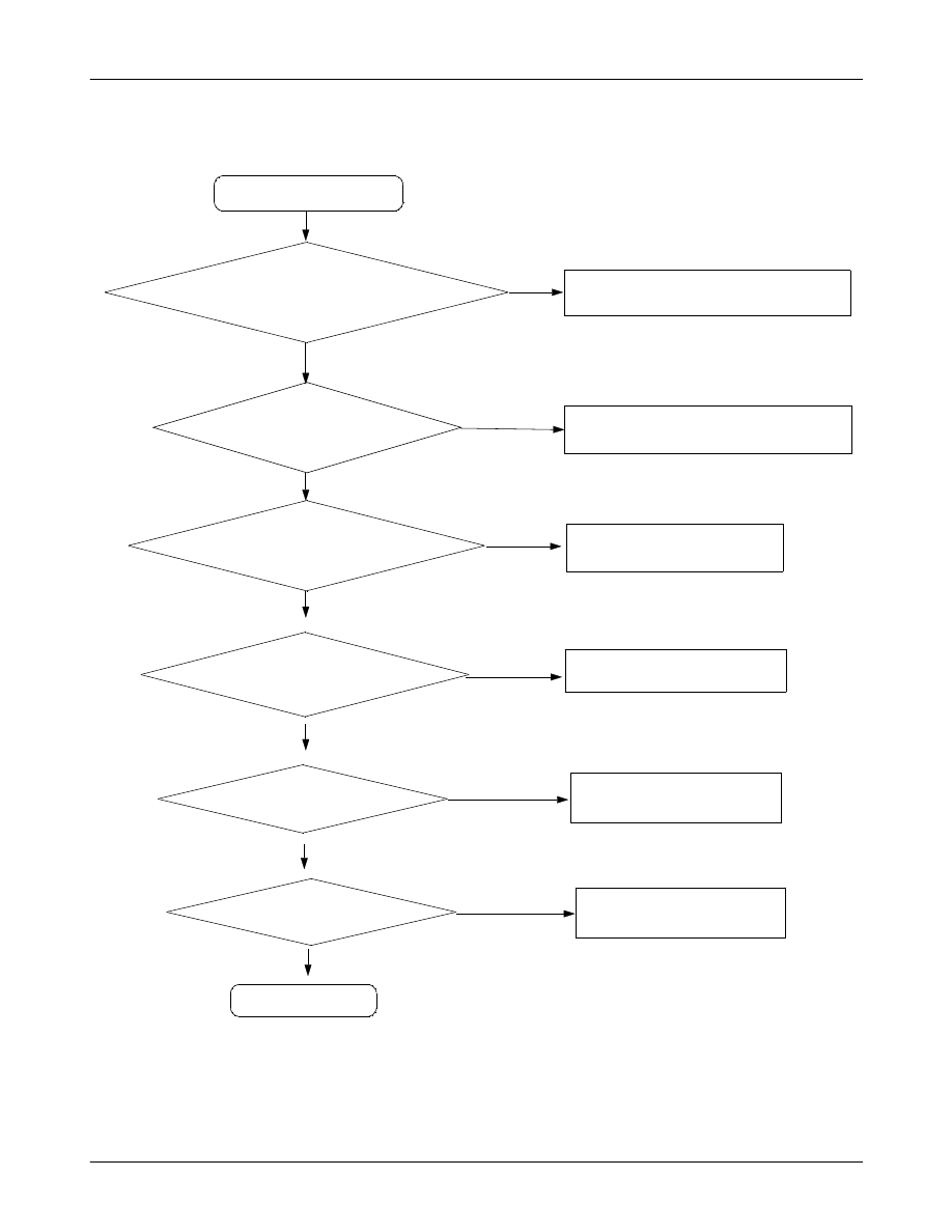
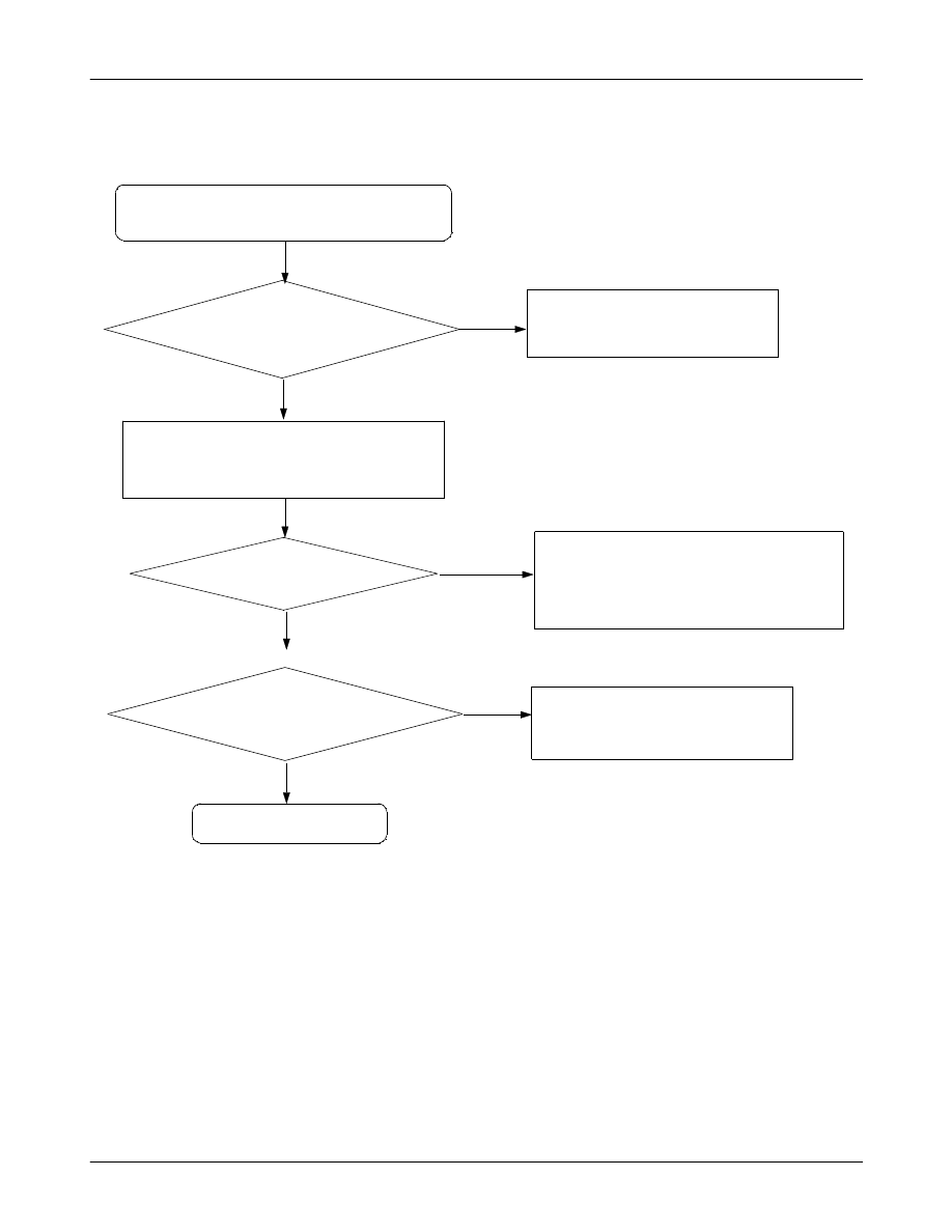
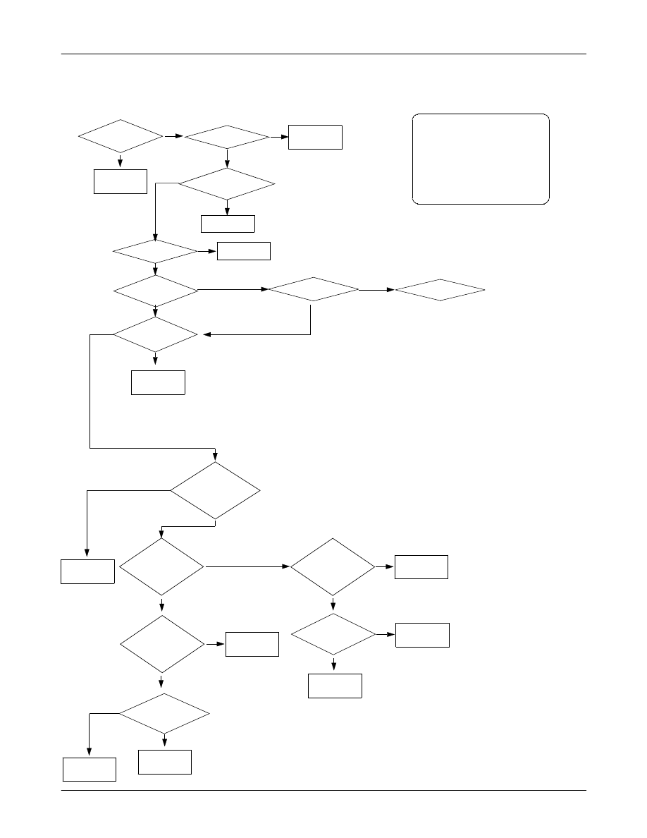
2. Initial
The pin#G11 of U101 = 1.8V
and
the pin#J12 of U101 ≒ 2.825V
?
Initialization Failure
Check the U101
(If it has some problem, adjust it.)
END
No
Yes
Is the pin#K9 of U101
"Low -> High"?
Yes
Check the U201
32.768kHz wave forms at
the C220 and C221
Check the LCD Part
Yes
No
Yes
Yes
The Voltage is "High" at
the C112
Check the Audio Part
No
Check the U101
(If it has some problem, adjust it.)
Check the U101
LCD display is O.K
No
No
Yes
Yes
Sound is O.K
No
SAMSUNG Proprietary-Contents may change without notice
Flow Chart of Troubleshooting
This Document can not be used without Samsung's authorization
7-3
, 1%
(rf-5000-6P-2.2L)
VCCD
C103
100NF
VCCB
2.2UF
16V
K12
VSI
M
VSS1G5
VSS2K4
VSS3R2
VSS4P6
VXVCM
R13
XOENAQ
D1
C111
G11
VLDO_2
J1
2
VLDO_3
A13
VLDO_4
B12
VLDO_5
B10
VLDO_6
A14
VLDO_7
C12
VREF
A10
VREGN
R14
VREGP
M13
VRTC
H11
VDD_IO1 N5
VDD_IO2 J4
VDD_OCTLC4
VEXT
E14
VIB_DRV
F15
VIB_RNG_EN
L9
A12
VL4S_A
VL4S_B
B11
VL5S_A
D10
VL5S_B
C9
VLDO_1
E13
J3
VDD1
VDD12
J1
3
VDD2 M3
VDD3 N6
VDD34
C11
VDD5 C10
VDD67 B13
VDDB A6
VDDD N11
VDDV L11
SERDA
B1
SERLE1
A2
SERLE2
SIM_CLK
K14
SIM_IO
J1
1
K11
SIM_RST
TXP
E7
N9
UP_CLK
UP_I
O
P10
UP_RST
R10
VACC
F14
VBAT
RTC_CLK
N4
RW
N
L2
RXTXI
N
D6
D7
RXTXI
P
RXTXQN
C6
RXTXQP
C7
SCLK_PSC
L8
SDI_PSC
M7
SDO_PSC
N7
SERCK
C2
C1
OCTL7
PSW1_BUF
L7
PWR_KEEP
M9
PWR_SW1N
C15
PWR_SW
2
C14
RAREF1
B6
RAREF2
B5
R3
RESETN_CSP
K9
RESET_O
F13
RING_DRV
H10
RTC_ALM
N
1
NC5
NC6 2
NC7
P5
OCTL0
E6
C5
OCTL1
OCTL2
F5
E5
OCTL3
A4
OCTL4
OCTL5
G6
OCTL6
B3
A3
GND_PSC2K15
INTRQ
L10
L3
I|O
LED1_DRV
G13
LED2_DRV
G12
MC
R6
MICINN
M14
MICINP
N14
MICOUTN
P15
MICOUTP
N15
MODE
N10
GNDS3 F9
GNDS4 F10
GNDS5 G7
GNDS6 G8
GNDS7 G9
GNDS8 G10
GNDS9 H6
GNDV P13
GND_HCURF11
GND_OCTLB4
GND_PSC1B15
E8
GNDS1 F7
H7
GNDS10
GNDS11 H8
H9
GNDS12
GNDS13 J7
GNDS14 J8
GNDS15 J9
GNDS16 J10
K10
GNDS17
GNDS2 F8
J5
DB3
J6
DB4
DB5
H5
G3
DB6
DB7
G4
DB8
F4
DB9
F1
DINTR
P3
GNDB F6
GNDD M10
GNDQ
M6
DAIRN
P4
DB0
K1
DB1
K2
F2
DB10
DB11
F3
DB12
E2
DB13
E3
DB14
D3
D2
DB15
DB2
K3
AUXOUTN
L13
AUXOUTP
K13
D13
AUX_ADC3
CH_BDRV
E11
CH_ISEN
F12
CH_RES
D14
E9
CREF
K8
CSN_PSC
R4
DAICK
DAIDI
L6
DAIDO
K7
AB7
AB8
K5
ADC_AUX1
E10
ADC_AUX2
D15
D9
AFC
AOUTAN
N12
AOUTAP
P11
AOUTBN
P12
AOUTBP
R12
AUXINN
L14
AUXINP
M15
CSP2200B1
U101
AB0
K6
P1
AB1
L5
AB2
N1
AB3
AB4
N2
M2
AB5
M1
AB6
R105
0
VR
F
100
R113
VBAT
C118
220NF
10K
R110
0
R104
VBAT
100PF
C110
C119
100NF
2.2UF
C112
C120
1UF
6.3V
1.2K
R101
16V
10K
R109
NC
R115
11
GG
12
GND
3
2
IN
4
ISET
VL
1
6
_ACOK
8
_CHG
_EN
5
U107
MAX1508ETA
BATT
7
9
G
10
G
VCCD
R112
100K
C123
10UF
10V
16V
2.2UF
C116
0
R103
100
R102
33PF
C107
TP103
470NF
C113
TP102
AGND
7
NC
8
NC
9
NC
10
NC
VCC
1
VCC
2
VPP
5
AGND
CN101
5000-6P-2.2L
CLK
3
GND
4
6
I/O
RB414_IV02N
BAT101
NEG
2
PO
S
1
AGND
100NF
C106
470nF
C121
AGND
100NF
C117
R108
0
VCCD
VCCA
10V
2.2UF
C104
R114
100K
VRT
C
VCCD
C101
56PF
VCC_1.8A
R106
0
DTC144EM
Q102
1
3
2
C109
33PF
TP104
C124
4
Y
100NF
VBAT
TC7S32FU
U102
2
A
1
B
3
GND
5
VCC
R111
100K
TP105
C115
1UF
6.3V
VCCD
VCCA
10V
2.2UF
C105
56PF
C102
C108
33PF
AGND
C122
470nF
TP106
56PF
C114
FL_LED
JIG_ON
TA_VEXT
R107
2.7K
VIB_EN
GSM_TX_EN
DCS_TX_EN
VREF
RXTXI
N
RXTXI
P
RXTXQ
N
RXTXQ
P
UP_SCLK
UP_SDI
TXPOWER
SIMCLK
SIMDATA
SIMRST
BL_KEY_LED
CLK13M_M
C
MICINN
MICINP
MICOUTN
MICOUTP
PWR_KEEP
PWR_ON
RST
RTCALARM
CLK32K
CHG_ON
CHG_DET
TA_VEXT
AFC
AOUTAN
AOUTAP
UP_CS
DSP_INT
DSP_AB(7)
DSP_AB(6)
DSP_AB(5)
DSP_AB(4)
DSP_AB(3)
DSP_AB(2)
DSP_AB(1)
DSP_AB(0)
VBAT
MELODY_VI
B
DSP_DB(8)
DSP_DB(7)
DSP_DB(6)
DSP_DB(5)
DSP_DB(4)
DSP_DB(3)
DSP_DB(2)
DSP_DB(15)
DSP_DB(14)
DSP_DB(13)
DSP_DB(12)
DSP_DB(11)
DSP_DB(10)
DSP_DB(1)
DSP_DB(0)
DSP_AB(8)
ICHRG
SERLE
DSP_RW
N
FLASH_RESET
TX_EN
SI_EN
TX_BAND_SEL
XOENA
DSP_I
O
DSP_DB(9)
SERCLK
SERDAT
DSP_AB(0:8)
DSP_DB(0:15)
KEY_COL(2)
KEY_ROW(0
)
INTRQ
SAMSUNG Proprietary-Contents may change without notice
This Document can not be used without Samsung's authorization
Flow Chart of Troubleshooting
7-4
3. SIM Part
Are there any Signals at
pin#N9, #R10, #P10 of U101?
"Insert SIM" is displayed on the LCD
Check the U102
Check the SIM Card
END
No
Yes
Yes
Yes
No
Check the U101
Are there any Signals at
pin#K12, #K11, #K14, #J11 of
CN101?
SAMSUNG Proprietary-Contents may change without notice
Flow Chart of Troubleshooting
This Document can not be used without Samsung's authorization
7-5
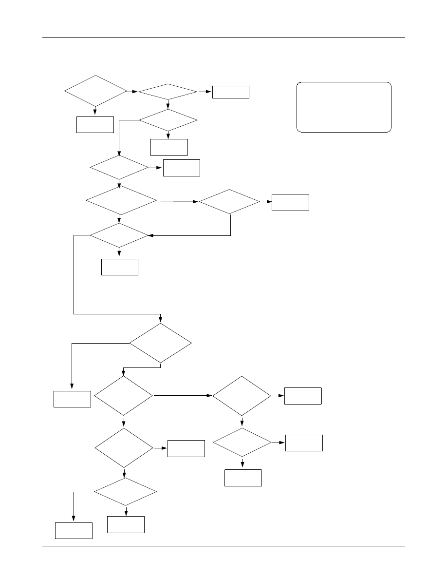
4. Charging Part
The pin#17, #18 of
CN601 is TA_VEXT ≒
5V ?
Abnormal charging operation
Replace TA or Check CN601
No
END
Yes
The pin#7 of U107 >=3.3V?
Check the U107
No
Yes
No
Solder again or change R107
Yes
The ICHRG = 1.4V(during
charging) and ≒ 180mV(full
charging) ?
SAMSUNG Proprietary-Contents may change without notice
This Document can not be used without Samsung's authorization
Flow Chart of Troubleshooting
7-6
C506
330NF
100NF
C515
C521
R510
10K
330NF
VBAT
OBG-415L44-C33P
MIC501
D501
RB520S-30
VCCD
33K
R506
NC
C528
33
R502
1UF
VBAT
10V
C523
C517
NC
C520
NC
100K
R511
TP502
NC
R518
0
C527
VBAT
R503
33
100PF
C502
ZD501
RSB6.8S-TE61
RSB6.8S-TE61
ZD502
R517
680
C511
6.3V
4.7UF
1K
R515
9
8
VSS
/IRQ
34
/RST
/W
R
28
C507
22NF
29
SDIN
32
SDOUT
SPOUT1
17
18
SPOUT2
SPVDD
15
16
SPVSS
SYNC
30
VDD
7
VREF
34
35
G
G
36
10
HPOUT-L/MONO
HPOUT-
R
11
IFSEL
56
PLLC
31
SCLK
D6
20
D7
12
EQ1
EQ2
13
14
EQ3
2
EXT1
EXT2
19
33
G
G
CLKI
1
27
D0
D1
26
D2
25
24
D3
D4
23
22
D5
21
C501
YMU759-QE2
U502
100NF
R516
1K
100K
R501
3.3K
R507
100NF
C510
2
NO1
10
NO2
1
V+
C508
100PF
12
13
G
G
14
GND
6
4
IN
1
8
IN
2
5
NC1
7
NC2
MAX4684ETB
U501
COM1
3
COM
2
9
11
G
G
TP501
C535
NC
C503
33K
R505
100PF
TP504
C513
10K
R512
100NF
NC
C516
C504
270PF
C505
100PF
NC
R520
0
R521
C529
6.3V
33UF
NC
C533
0
R509
C530
10PF
C534
NC
R519
0
C512
VCCA
TP503
VCCA
1NF
150K
R504
10V
C509
4.7UF
R513
100K
C532
100NF
D(2)
D(6)
D(4)
VIB_EN
MSPK-
MSPK+
AUDIO_OUT_SEL
AOUTAN
AOUTAP
MICOUTP
MICOUTN
MICINP
MICINN
MELODY_VIB
YMU_EN
YMU_IRQ
CP_OEN
RST
CP_WEN
A(0)
CLK13M_YM
U
D(0)
D(1)
D(3)
D(5)
D(7)
MSPK+
MSPK-
SAMSUNG Proprietary-Contents may change without notice
Flow Chart of Troubleshooting
This Document can not be used without Samsung's authorization
7-7
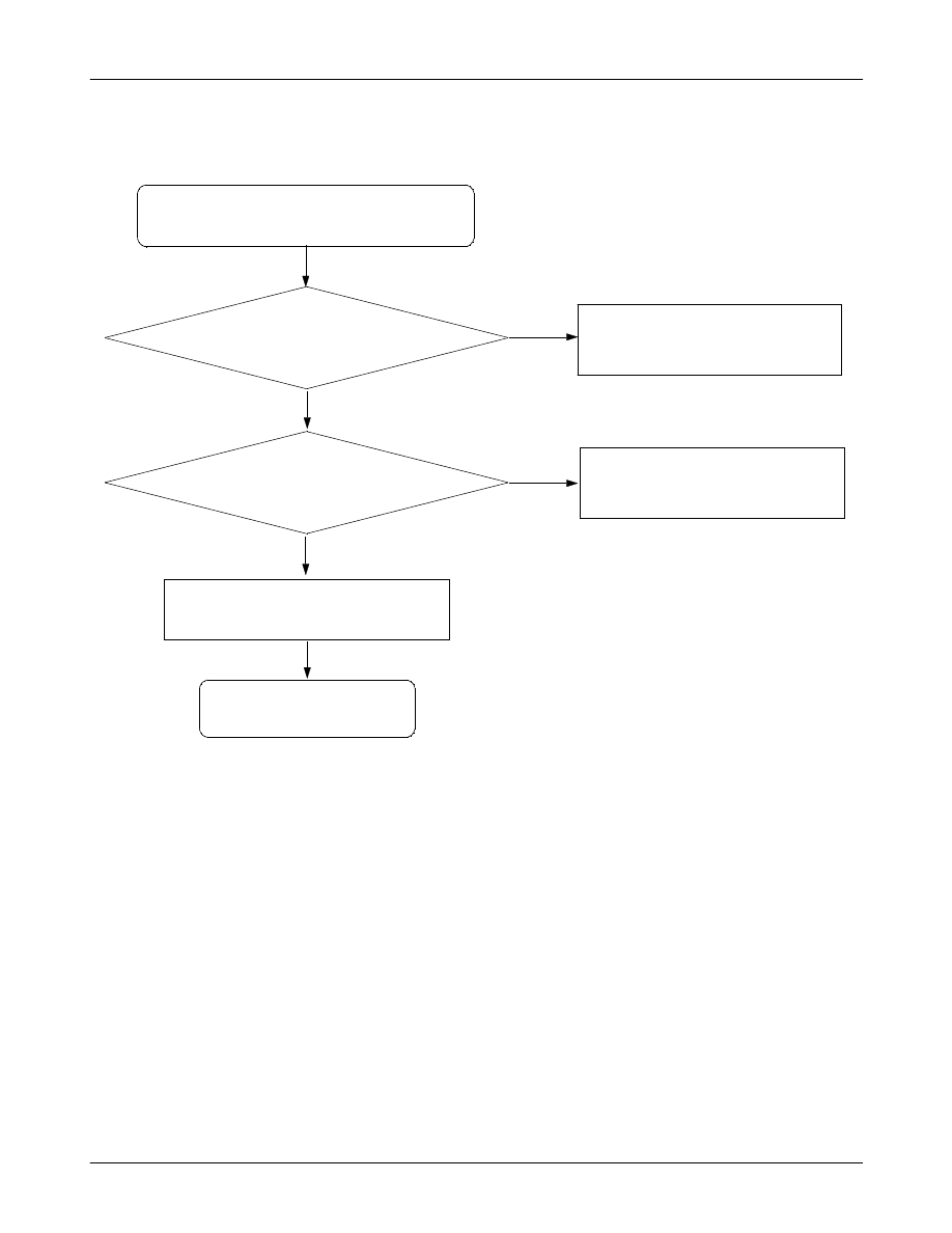
5. Microphone Part
Is the assembled status of
microphone O.K?
Microphone does not work
C529 > 2.5V
Reassemble the microphone
Solder the microphone again or
Replace around Mic Circuit
END
No
Yes
Yes
Yes
Yes
No
Is microphone ok ?
No
Check U101
Check the reference voltage on Mic path
SAMSUNG Proprietary-Contents may change without notice
This Document can not be used without Samsung's authorization
Flow Chart of Troubleshooting
7-8
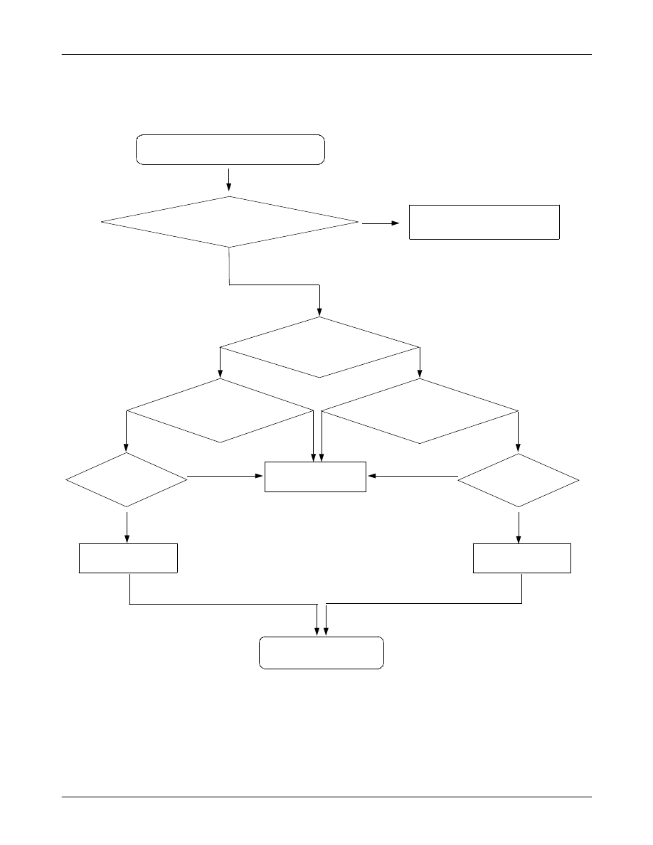
6. Speaker Part
Is the terminal of Speaker
O.K.?
There is no sound from Speaker
No
Replace the Speaker
The pin#4 of
U501 is
"Low"
Check U502
The pin#4 of
U501 is
"High"
Check U501
Are there any signals
at the pin#5 and
pin#7 of U501?
END
Yes
Yes
No
The type of sound
from the Speaker is
Melody
Yes
No
No
No
Yes
Yes
Yes
Are there any signals
at the pin#2 and
pin#10 of U501?
No
Check U101
SAMSUNG Proprietary-Contents may change without notice
Flow Chart of Troubleshooting
This Document can not be used without Samsung's authorization
7-9
C506
330NF
100NF
C515
C521
R510
10K
330NF
VBAT
OBG-415L44-C33P
MIC501
D501
RB520S-30
VCCD
33K
R506
NC
C528
33
R502
1UF
VBAT
10V
C523
C517
NC
C520
NC
100K
R511
TP502
NC
R518
0
C527
VBAT
R503
33
100PF
C502
ZD501
RSB6.8S-TE61
RSB6.8S-TE61
ZD502
R517
680
C511
6.3V
4.7UF
1K
R515
9
8
VSS
/IRQ
34
/RST
/W
R
28
C507
22NF
29
SDIN
32
SDOUT
SPOUT1
17
18
SPOUT2
SPVDD
15
16
SPVSS
SYNC
30
VDD
7
VREF
34
35
G
G
36
10
HPOUT-L/MONO
HPOUT-
R
11
IFSEL
56
PLLC
31
SCLK
D6
20
D7
12
EQ1
EQ2
13
14
EQ3
2
EXT1
EXT2
19
33
G
G
CLKI
1
27
D0
D1
26
D2
25
24
D3
D4
23
22
D5
21
C501
YMU759-QE2
U502
100NF
R516
1K
100K
R501
3.3K
R507
100NF
C510
2
NO1
10
NO2
1
V+
C508
100PF
12
13
G
G
14
GND
6
4
IN
1
8
IN
2
5
NC1
7
NC2
MAX4684ETB
U501
COM1
3
COM
2
9
11
G
G
TP501
C535
NC
C503
33K
R505
100PF
TP504
C513
10K
R512
100NF
NC
C516
C504
270PF
C505
100PF
NC
R520
0
R521
C529
6.3V
33UF
NC
C533
0
R509
C530
10PF
C534
NC
R519
0
C512
VCCA
TP503
VCCA
1NF
150K
R504
10V
C509
4.7UF
R513
100K
C532
100NF
D(2)
D(6)
D(4)
VIB_EN
MSPK-
MSPK+
AUDIO_OUT_SEL
AOUTAN
AOUTAP
MICOUTP
MICOUTN
MICINP
MICINN
MELODY_VIB
YMU_EN
YMU_IRQ
CP_OEN
RST
CP_WEN
A(0)
CLK13M_YM
U
D(0)
D(1)
D(3)
D(5)
D(7)
MSPK+
MSPK-
SAMSUNG Proprietary-Contents may change without notice
This Document can not be used without Samsung's authorization
Flow Chart of Troubleshooting
7-10
U402 CHECK
pin#8 ≥ -65dBm ?
8. GSM Reciever
CONTINUOUS RX ON
RF INPUT : 190CH
AMP : -50dBm
NORMAL CONDITION
catch the channel?
U404 CHECK
pin8 : 13MHz ?
Vp-p : 860mV?
U402 CHECK
pin#2,3 ≥ -65dBm ?
U404 CHECK
pin#20,21 ≥ -65dBm ?
Check soldered status of
R426,L402,C450
U401
resolder or change
U402
resolder or change
C408,L401,C409
resolder or change
OSC401 CHECK
clean 3V?
U404 CHECK
pin#9 : clean 3V?
U101 pin#39
check or resolder
U404 pin#1,2,3,28
Vp-p : 100mV?
U404
resolder or change
CHECK
U101
NO
YES
NO
NO
NO
NO
NO
NO
NO
YES
YES
YES
YES
YES
YES
OSC401 CHECK
13MHz ?
Vp-p : 950mV?
OSC401
Resolder or
Change?
YES
SAMSUNG Proprietary-Contents may change without notice
Flow Chart of Troubleshooting
This Document can not be used without Samsung's authorization
7-11
9. GSM transmitter
U402 pin#8 :
about 2~3 dBm?
U401, C407
check&change
U402
pin#1 : 3 V?
U101
check & change
C414
≒ 4~5dBm?
U403
check & change
C423 : 3.7 V?
NO
NO
YES
YES
YES
NO
NO
BATTERY, U404
check & change
Between
R402 & U403 :
1.2V?
YES
NO
R402
check & change
C434 :
≒ -5dBm ?
YES
YES
U403
change
U101
check & change
YES
NO
U404 pin#32
: 3V ?
U101 pin#C4
change or resolder
YES
U404
pin#4,5 : 1.7V ?
YES
U101
change
NO
NO
U404
change or resolder
YES
U404
pin#8 : 13MHz?
Vp-p: 950mV
U404
pin#9 : 3V?
YES
OSC401
pin#3 : 13MHz?
Vp-p : 950mV
OSC401
change or resolder
U101
check or change
0SC401
pin#4 : 3V ?
U101 pin#C4
change or resolder
U101
change or resolder
NO
NO
YES
NO
YES
NO
CONTINUS TX ON CONDITION
TX POWER DAC:500 CODE APPLIED
CH:190
RBW : 100KHz
VBW : 100KHz
SPAN : 10MHz
REF LEV. : 10dBm
ATT. : 20dB
NO

SAMSUNG Proprietary-Contents may change without notice
This Document can not be used without Samsung's authorization
Flow Chart of Troubleshooting
7-12
U402 CHECK
pin#8 ≥ -65dBm ?
10. PCS Receiver
CONTINUOUS RX ON
RF INPUT : 660 CH
AMP : -50dBm
NORMAL CONDITION
catch the channel?
U404 CHECK
pin#8 : 13MHz ?
Vp-p : 860mV?
U402 CHECK
pin#4,5 ≥ -65dBm ?
U404 CHECK
pin#16,17 ≥ -65dBm ?
Check soldered status of
R426, L402, C450
U401
resolder or change
U402
resolder or change
C411,L403,C413
resolder or change
OSC401 CHECK
clean 3V?
U404 CHECK
pin#9 : clean 3V?
U101 pin#39
check or resolder
U404 pin#1,2,3,28
Vp-p : 100mV?
U404
resolder or change
CHECK
U101
NO
YES
NO
NO
NO
NO
NO
NO
NO
YES
YES
YES
YES
YES
YES
YES
OSC401 CHECK
13MHz ?
Vp-p : 950mV?
OSC401
Resolder or
Change?
SAMSUNG Proprietary-Contents may change without notice
Flow Chart of Troubleshooting
This Document can not be used without Samsung's authorization
7-13
U404
change or resolder
11. PCS transmitter
U402 pin#8 :
about 2~3 dBm?
U401,C407
check&change
U402
pin#6 : 3 V?
U101
check & change
C435:
≒ 4~5dBm?
U403
check & change
C423 : 3.7 V?
NO
NO
YES
YES
YES
NO
NO
BATTERY, U404
check & change
Between
R402 & U403
: 1.2V?
YES
NO
R402
check & change
NO
C436:
≒ -5dBm ?
YES
YES
YES
U101
check
NO
U404 pin#32
: 3V ?
U101 pin#39
change or resolder
YES
U404
pin#4,5 : 1.7V ?
U101
change
NO
NO
U404
change or resolder
YES
U404
pin#8 : 13MHz?
Vp-p : 950mV
U404
pin#9 : 3V?
YES
YES
OSC401
13MHz?
Vp-p : 950mV
OSC401
change or resolder
U101
check or change
OSC401
pin#4 : 3V ?
U101 pin#39
change or resolder
U101
change or resolder
NO
NO
YES
NO
YES
NO
CONTINUOUS TX ON CONDITION
CH : 660CH(PCS)
TX POWER CODE: 350 CODE Aplied
RBW : 100KHz
VBW : 100KHz
SPAN : 10MHz
REF LEV. : 10dBm
ATT. : 20dB
SAMSUNG Proprietary-Contents may change without notice
This Document can not be used without Samsung's authorization
Flow Chart of Troubleshooting
7-14
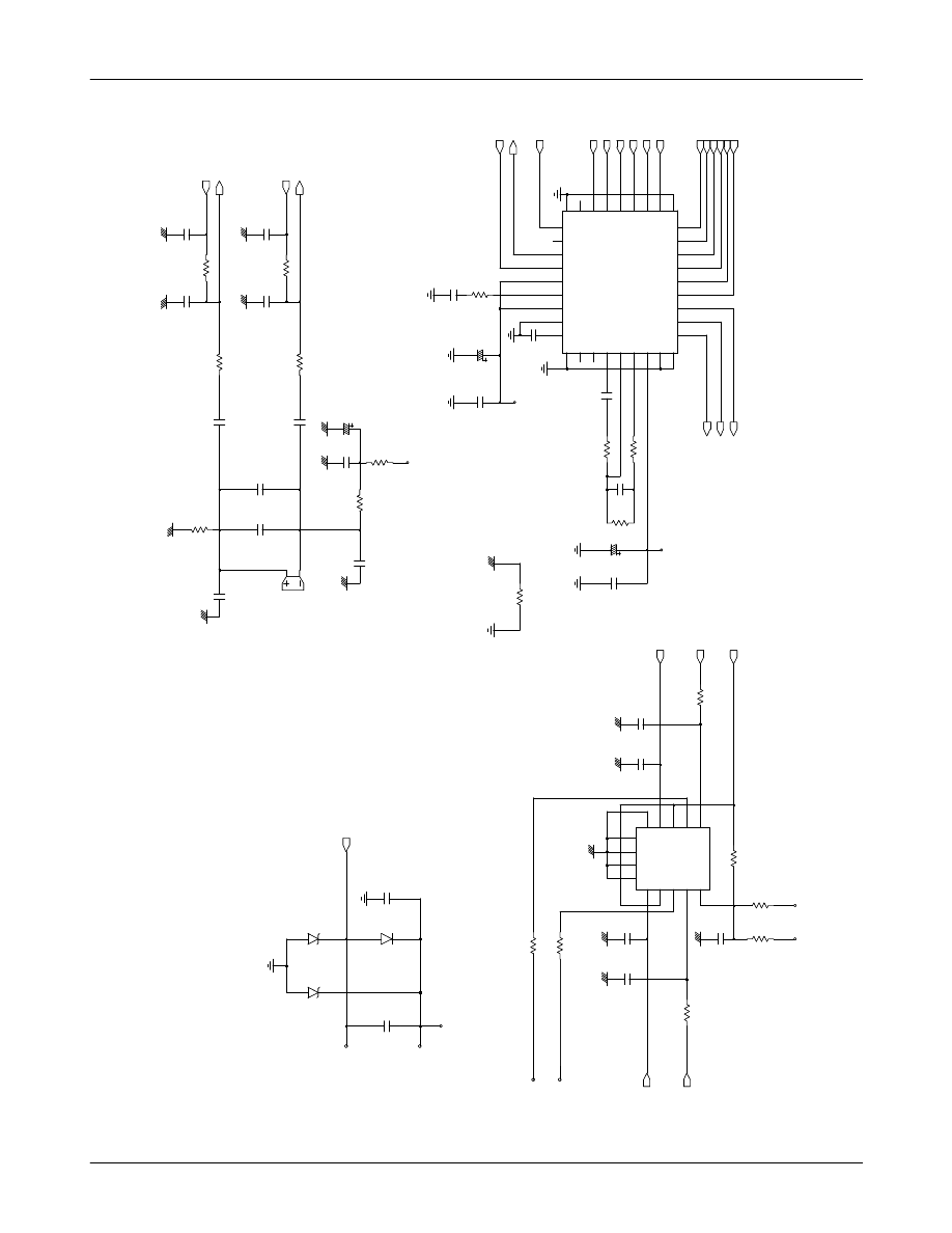
R424
100
1
IN
2
OUT
R422
12
U401
MS-156(02)
G1
3
G2
4
100NF
C422
10NF
C443
6.3V
22UF
C417
C431
100PF
C402
100PF
6.3V
C433
22UF
22PF
C410
C430
100PF
33PF
C436
VBAT
C435
22PF
VRF
R421
L402
33nH
R420
2.2K
560
10NF
PCS-RX
5
PCS-TX
11
VC1
1
6
VC2
C419
G
91
0
GG
12
G
14
GSM-R
X
2
3
GSM-R
X
GSM-T
X
13
4
PCS-RX
U402
LMSP54KA-246TEMP
8
ANT
G
7
C429
100PF
10K
C434
R423
1PF
C408
47PF
GND
2
OUT
3
4
VCC
VT
1
VC-TCXO-208C3
OSC401
L401
33nH
C411
1.5PF
C412
NC
C437
NC
VR
F
100PF
C440
18PF
C439
C409
1PF
1.5PF
C413
L405
33nH
NC
C452
10NF
C438
17
1
GSM850/900I
N
14
GSM850/900OUT
TX_EN
6
5
VBATT
12
VCC
4
VRAM
P
2
GND
GND
38
GND
GND
11
13
GND
GND
15
16
GND
GND
TQM7M4022
U403
7
BS
9
DCS/PCSI
N
10
DCS/PCSOUT
C414
47PF
10NF
C442
6.3V
100UF
C406
ANT2
NC
C404
100PF
C423
R426
0
NC
C453
NC
5.6nH
L403
L404
22PF
C407
10NF
C441
C401
100PF
26
XEN
8
XIN
27
XOUT
10
_PDN
12
_SEN
14
SDI
11
SDO
5
TXI
N
4
TXI
P
7
TXQN
6
TXQP
9
VDD
32
VDD
16
RFIPP
22
RFOD
23
RFOG
3
RXI
N
RXI
P
2
1
RXQN
28
RXQP
13
SCLK
GND 34
35
GND
GND
36
19
RFIDN
18
RFIDP
21
RFIGN
20
RFIGP
17
RFIPN
24
DIAG1
25
DIAG2
15
GND
29
GND
GND 30
31
GND
GND 33
27K,1%
U404
SI4205-BMF
2.7PF
R402
C450
0
R425
C449
10NF
SERLE
10NF C418
ANT
RXTXI
N
RXTXI
P
RXTXQN
RXTXQP
SERCLK
SERDAT
XOENA
CLK13M_RF
13MHZ_SI
SI_EN
GSM_PAM_I
N
DPCS_PAM_I
N
GSM_LNA_IN_P
GSM_LNA_IN_N
DCS_TX_EN
PCS_LNA_IN_P
PCS_LNA_IN_N
GSM_TX_OUT
TX_EN
GSM_PAM_I
N
DPCS_PAM_I
N
TX_BAND_SEL
AFC
CLK13M_RF
CLK13M_M
C
CLK13M_TR
13MHZ_SI
CLK13M_YM
U
GSM_TX_OUT
DCS_TX_OUT
PCS_LNA_IN_P
PCS_LNA_IN_N
GSM_LNA_IN_N
GSM_LNA_IN_P
GSM_TX_EN
DCS_TX_OUT
TXPOWER
Wyszukiwarka
Podobne podstrony:
Samsung SGH R200 service manual
Samsung SGH E710 service manual
Samsung SGH T500 service manual
Samsung SGH A408 service manual
Samsung SGH Q208 service manual
Samsung SGH N288 service manual
Samsung SGH A288 service manual
Samsung SGH S341i service manual
Samsung SGH E715 service manual
Samsung SGH X120 service manual
Samsung SGH Q100 service manual
Samsung SGH 2400 service manual
Samsung SGH N200 service manual
Samsung SGH R220E service manual
Samsung SGH Q105 service manual
Samsung SGH D410 service manual
Samsung SGH A200 service manual
więcej podobnych podstron