
13
Mask for Proximity X-Ray Lithography
Masatoshi Oda and Hideo Yoshihara
CONTENTS
13.1 PXL System
13.2 X-Ray Mask Structure
13.2.1 Membrane
13.2.2 Absorber
13.3.1 Mask Processes
13.3.2 EB Writing
13.3.3 Dry Etching
13.3.4 Frame Bonding
13.4 Defect Inspection and Repair
13.5 X-Ray Masks for LSI Fabrication
13.6 Summary
References
Proximity x-ray lithography (PXL) was proposed 30 years ago as a technology to perfectly
replicate mask patterns to a wafer using soft x-rays [1]. Although the PXL was confirmed
to have sufficient resolution to form patterns below 100 nm soon after its proposal [2], it
could not be used in industry for a long time because x-ray sources were too weak and
mask fabrication was too difficult. The development of a compact synchrotron radiation
(SR) ring [3] gave the industry an x-ray source that could produce x-rays at an intensity
strong enough for practical use. The SR ring together with improved mask technology has
made PXL the most promising technology for making sub-100-nm patterns. Here, x-ray
mask technology is introduced.
13.1
PXL System
A PXL system consists of an x-ray source, a mask, and a stepper, and uses soft x-rays with
wavelengths between 0.5 and 1.5 nm. x-rays with shorter wavelengths are not suitable
because their higher transparency makes both resist sensitivity and mask contrast too
low. On the other hand, x-rays at longer wavelength degrade pattern resolution due to the
large diffraction.
Rizvi / Handbook of Photomask Manufacturing Technology DK2192_c013 Final Proof page 305 7.3.2005 6:25pm
© 2005 by Taylor & Francis Group.
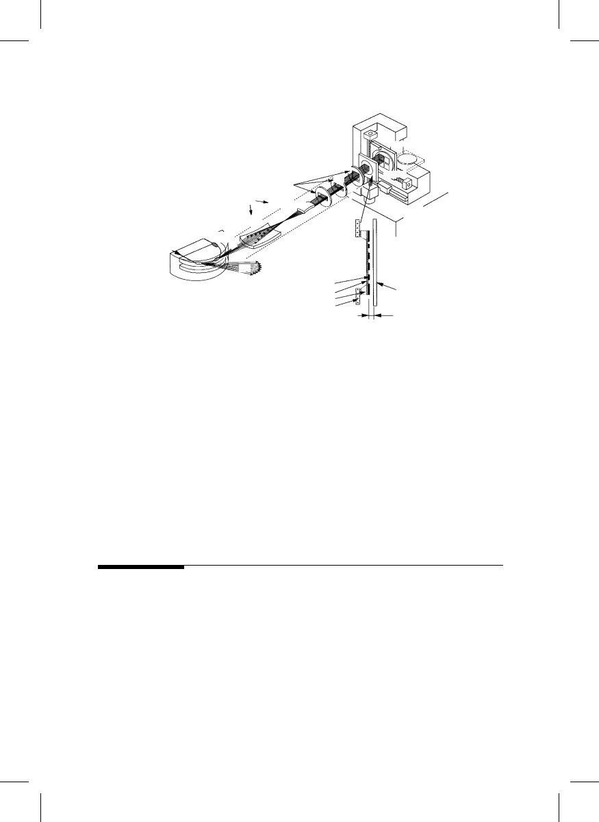
Figure 13.1 shows a PXL system using an SR ring. In this SR lithography system, x-rays
from the SR ring are directed to the mask through a beam line. A wafer coated with resist
is set behind the mask leaving a small proximity gap of the order of a few ten microm-
eters. The stepper aligns the wafer.
In PXL, the objective is to replicate to the wafer patterns that are of the same size as the
mask patterns. Thus, the mask patterns must be of the right size and all features must be
at right locations according to the design layout.
Furthermore, the substrate must be thin enough to allow maximum transmission of the
soft x-rays. On the other hand, the absorbers have to be thick enough to stop the x-rays
from reaching the wafer. The biggest issue is how to produce absorber patterns with high
accuracy on such a thin membrane.
13.2
X-Ray Mask Structure
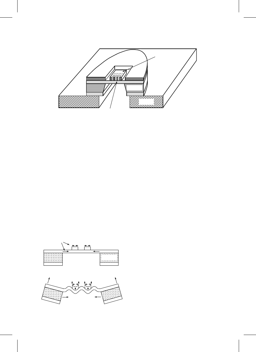
X-ray masks differ significantly in construction from the photomasks. An x-ray mask
consists of absorber patterns on a membrane held by a Si wafer, as shown in
where the Si wafer is mounted on a frame. The membrane corresponds to the glass
substrate of a photomask. The frame is made of materials having high rigidity, such as
Pyrex glass or SiC, which is needed so that the masks can be easily and safely handled.
For the membrane to stay flat, it must have tensile stress. The absorber patterns also
have stresses, though they are produced unintentionally. These stresses tend to deform
the mask as shown in
The deformation must be very small so that it does not
affect the accuracy of the x-ray masks. To keep the Si wafer from being deformed by
membrane stress, Si wafers as thick as 2 mm are used. Absorber stress must also be kept
small so as not to deform the membrane.
X-ray extraction window
X-ray mirror
Beam
convergence
High
vacuum
SiN
He
Vertical
x
−
y
stage
Ultra-high vacuum
Beamline
X-ray stepper
X-ray mask
X-ray source
(SR ring)
Wafer
10
−
30
µ
m
Absorber
Membrane
Si wafer
Frame
Scanning
SR
Electron
SR
Be
Wafer
FIGURE 13.1
Schematic of the SR lithography system.
© 2005 by Taylor & Francis Group.
13.2.1 Membrane
The essential membrane requirements are as follows: (a) high transparency to soft x-rays,
(b) good smoothness, (c) good flatness, (d) high dimensional stability, (e) high mechanical
strength, (f) high chemical durability, (g) high optical transparency, and (h) ease of
fabrication. To achieve high x-ray transparency, the membrane material must be made
of light elements with small x-ray absorption coefficients. Recently used membrane
materials are Si, SiN, SiC, and diamond (
In addition to these materials,
organic films, such as Mylar, have also been studied. Organic films, however, suffer
from dimensional and thermal stability problems.
The deposition of SiN [4] and SiC [5] is carried out by low-pressure (LP) CVD, whereas
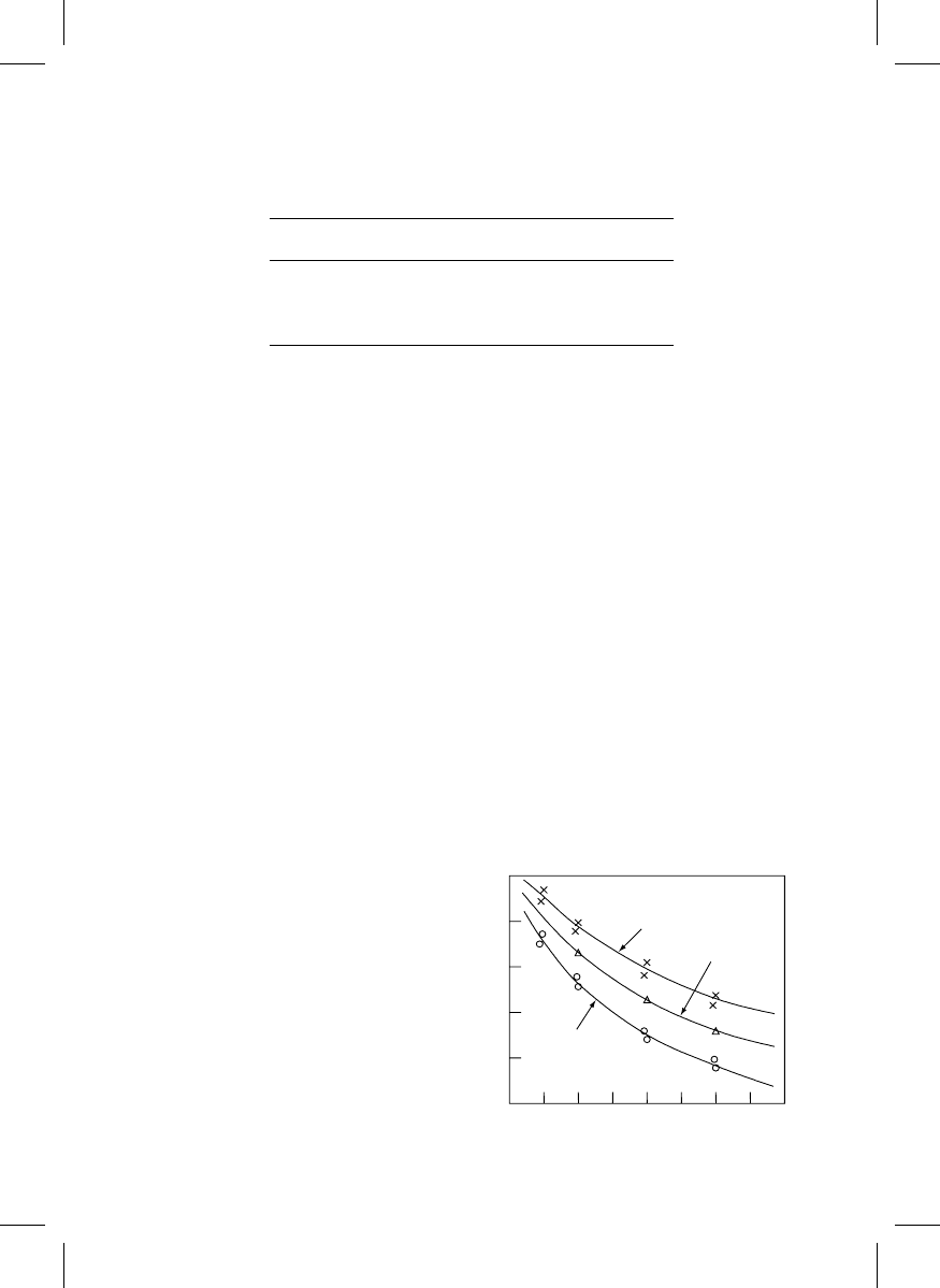
the deposition of diamond is typically done by microwave plasma CVD [6]. The stress of a
SiN film can be easily controlled by adjusting the temperature and gas flow ratio during
low-pressure CVD as shown in
[4]. Films with low tensile stress are deposited
at high temperatures or at a large NH
3
flow rate. The stresses of SiC and diamond can also
be controlled by adjusting deposition conditions. SiN is amorphous, so the film surface is
smooth after deposition. On the other hand, SiC [7] and diamond [6] are poly-crystals, so
Absorber patterns
Frame
Membrane
Si wafer
FIGURE 13.2
Schematic of an x-ray mask.
Si frame
Membrane
Absorber
Stress
(a) Stress
(b) Deformation
FIGURE 13.3
Membrane and absorber stress, and mask deformation
caused by the stress.
© 2005 by Taylor & Francis Group.
the surfaces are rough due to crystal grains. The roughness is removed by mechanical
polishing after deposition.
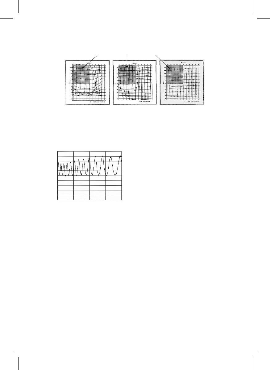
shows deformation of SiN, SiC, and diamond membranes caused by Ta
absorber stress. As the absorber patterns having compressive stress of about 30 MPa at the
upper left spread, the membranes deform. The deformation decreases as the membrane’s
Young’s modulus increases, and the smallest deformation is in the diamond membrane.
Young’s modulus is thus a very important factor for highly accurate masks.
For highly accurate optical alignment, highly optical transparency is needed. Figure
13.6 shows the transparency of diamond membrane for wavelengths ranging from 400 to
800 nm. The transparency varies periodically with wavelength, which results from inter-
ference from light reflected at the surfaces. The transparency can be improved to over 80%
at every wavelength between 500 and 800 nm by depositing antireflection material, such
as SiO
2
, on both sides of the membrane.
The membrane must have enough durability for x-rays. When the membrane contains
hydrogen atoms from the deposition source gasses, the stress and transparency are varied
by x-ray exposure [8]. It has been reported that SiC and diamond with good film quality
have good x-ray durability.
Unlike the Si-based materials in Table 13.1, the diamond does not have an x-ray
absorption edge near 0.7 nm because it has no Si element. Thus, x-rays having wave-
lengths shorter than 0.7 nm can be used.
Recently, it was reported that such short-wavelength x-rays make it possible to repli-
cate patterns smaller than a nanometer. The PXLs with short-wavelength x-rays are
referred as second-generation PXL [9].
TABLE 13.1
Properties of Membrane Materials
Young’s
Modulus (GPa)
Thermal Expansion
Coefficient (deg
1
)
Density
(g/cm
3
)
Si
160
3.7 10
6
2.33
SiN
160
2.1 10
6
3.18
SiC
460
4.6 10
6
3.21
Diamond
1050
3.5 10
6
3.52
FIGURE 13.4
SiN stress and deposition condition of low-pres-
sure CVD.
850
⬚
C
750
⬚
C
800
⬚
C
−
200
0
200
400
600
800
Stress (MPa)
(Tensile)
0
1
2
3
4
5
6
7
8
Gas flow ratio (SiH
2
Cl
2
/NH
3
)
Rizvi / Handbook of Photomask Manufacturing Technology DK2192_c013 Final Proof page 308 7.3.2005 6:25pm
© 2005 by Taylor & Francis Group.
13.2.2 Absorber
The required absorber properties are as follows: (a) a high absorption coefficient, (b) high
stress controllability, (c) capability of patterning below 100 nm, (d) high chemical and
radiation durability, and (e) the ease of fabrication. The high absorption coefficient
requirement is met by using high-density heavy metals as absorber. Au has been used
as an absorber material since the beginning of x-ray mask development [10] because it has
a large x-ray absorption coefficient, and fine patterns can easily be formed. Recently, Ta
[11], W [12], and their compounds [13,14] have been used as absorber materials, which
can be patterned by dry etching [11–14]. These materials have approximately the same
absorption coefficient as gold at x-ray wavelengths ranging from 0.5 to 1.5 nm. Physical
properties of absorber materials are summarized in
Absorber stress must be small so that it does not cause membrane distortion (
Generally, in films deposited by sputtering, the stress can be controlled by the
pressure during deposition.
shows the dependence of films’ (Ta, W, and Re)
stress on pressure. For each material, the stress changes from compressive to tensile, as
the pressure increases. For Ta, the tensile stress reduces again with pressure and is zero at
around 8.5 Pa. The stress of W and Re also comes close to zero when in the high-pressure
region. However, stress-free Ta film deposited at high pressure has smaller density than
30-MPa compressive absorber area
SiN (Max: 239 nm)
SiC (Max: 112 nm)
Diamond (Max: 56 nm)
FIGURE 13.5
Membrane material and its deformation caused by absorber stress.
400
500
600
700
800
0
50
100
Wavelength ( nm)
Transmittance (%)
FIGURE 13.6
Optical transmittance of diamond membrane.
© 2005 by Taylor & Francis Group.
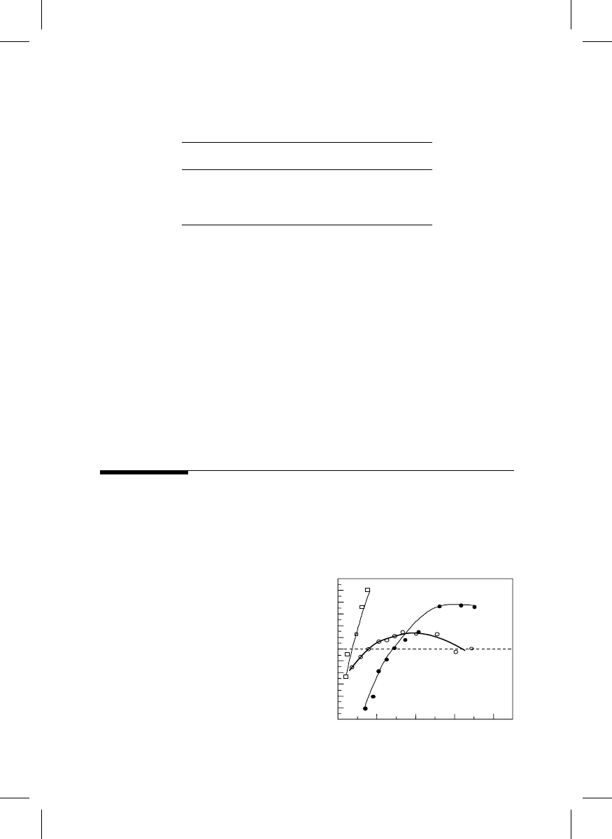
that deposited at low pressure. Thus, the low-pressure region is used for depositing Ta
absorber films. In Figure 13.7, the gradient of the stress–pressure curve near the stress-free
point is smaller for Ta than for Re or W, indicating the stress in Ta film can be controlled
more precisely.
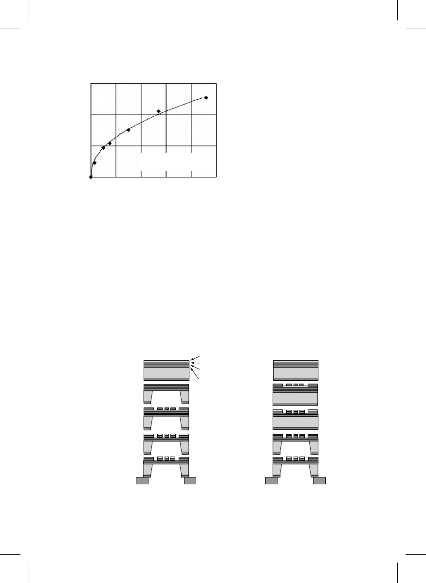
To control the stress even more precisely, annealing is performed after deposition. The
stress in Ta film shifts to compressive side by annealing as shown in
Ta films
deposited by sputtering have columnar grains. Oxygen diffuses along the grain bound-
aries from the film surface and causes oxidation in Ta films, making the stress compres-
sive. Stress-free Ta films can be obtained by depositing tensile films after annealing for an
appropriate time.
The stress in Ta or W compounds having an amorphous structure is more stable. These
films can also be deposited by sputtering, and stress control can be done in the same way
as for Ta film. However, contrary to Ta, the stress changes from compressive to tensile by
annealing [13].
13.3
Fabrication
The key areas in the fabrication of x-ray masks are: (1) processing (2) e-beam writing,
(3) dry etching, and (4) frame bonding, discussed in the following.
TABLE 13.2
Properties of Absorber Materials
Young’s
Modulus (GPa)
Thermal Expansion
Coefficient (deg
1
)
Density
(g/cm
3
)
Au
88
1.5 10
5
19.3
Ta
190
6.5 10
6
16.7
W
410
4.6 10
6
19.3
WTi, TaBN
—
—
15–16
FIGURE 13.7
Film stress and gas pressure during sputtering.
10
8
6
4
2
Re
Ta
W
Pressure (Pa)
Compressive
Stress (MPa)
0
200
400
600
800
1000
1200
−
400
−
600
−
800
−
1000
−
1200
−
200
Tensile
© 2005 by Taylor & Francis Group.
13.3.1 Mask Processes
There are two processes for making x-ray masks. One is a membrane process, in which
absorber patterning is carried out after back-etching [Figure 13.9(a)]. The other is a wafer
process, in which absorber patterning is done before back-etching [Figure 13.9(b)]. In the
wafer process, no membrane breakage occurs. However, improving the pattern place-
ment accuracy is difficult because large pattern shifts occurs during back-etching. In the
membrane process, masks with high pattern-placement accuracy can be produced, al-
though the apparatus must have special functions for handling wafers with a membrane.
In recent days, the membrane process has been mostly favored because the process leads
to highly accurate masks.
As shown in Figure 13.9(a), a 2-mm-thick SiC or diamond film is deposited on a 4-in. Si
wafer. A Ru film is deposited on the membrane to a thickness of 20 nm by sputtering.
Then Ta film is deposited on Ru by ECR-sputtering. Following this, SiO
2
is then deposited
on Ta by using ECR-plasma CVD technique. The Ru film stabilizes Ta stress [15], and the
0
20
40
60
80
100
0
50
100
150
Annealing time (min)
Stress change (MPa)
Ta thickness: 0.55
µ
m
Temperature: 250
⬚
C
FIGURE 13.8
Stress change of Ta film caused by annealing in
air.
ECR-Ta
Ru
SiC or
diamond
SiO
2
(a) Membrane process
(b) Wafer process
Deposition
Back-etching
EB writing
Etching
Frame bonding
Deposition
Back-etching
EB writing
Etching
Frame bonding
FIGURE 13.9
X-ray mask fabrication process.
© 2005 by Taylor & Francis Group.

SiO
2
is used as a mask for Ta etching. After the deposition of these films, back-etching is
carried out using KOH solution. Resist patterns are formed on the membrane with an
electron beam (EB) writer and the SiO
2
film is etched by reactive ion etching. Next, the Ta
film is etched using the SiO
2
as a mask. Finally, the Si wafer is bonded to a glass frame. In
the wafer process in
x-ray masks are produced using similar deposition
and patterning techniques.
To produce highly accurate x-ray masks, one can correct pattern position shifts by a
method known as previous analysis of distortion and transformation (PAT) of coordin-
ates [16] or product-specific emulation (PSE) [17]. In this method, first, send-ahead masks
are made to obtain information about pattern position shifts. Next, working masks are
produced by an EB writing process, in which patterns are delineated so as to compensate
for the pattern position shifts. If the pattern position shifts are sufficiently reproducible,
very highly accurate masks can be made. Nippon Telegraph and Telephone Corporation
(NTT) has produced x-ray masks with feature-placement accuracy below 25 nm by using
this method [18].
The membrane process has three key operations: EB writing to form resist patterns on
the thin membrane with high accuracy, etching of absorber film on the membrane, and
the frame bonding.
13.3.2 EB Writing
EB writing must be performed on a thin membrane supporting a heavy metal absorber.
Electrons scattering from the absorber strongly affect the formation of resist patterns.
Therefore, an EB writer with acceleration voltage of 100 keV was developed, which is
significantly higher than the conventional 30 keV systems (
[19]. This EB
writer can form resist patterns with a width of 50 nm. The high resolution comes from the
excellent beam sharpness and small forward-scattering in the resist film. Due to the high
acceleration voltage, most of the electrons pass through the membrane. The small num-
bers of electrons that scatter backward in the absorber disperse widely. Therefore, the
proximity effect is very small. Using this writer, even complex fine patterns, such as LSI
patterns (more complex than 4-Gbits DRAMs), can be formed with a large margin [14].
The mask holder for the EB writer must be designed carefully. The surface of the holder
has to be such that electrons passing through the membrane do not scatter backward [20].
13.3.3 Dry Etching
In an x-ray mask, pattern width precision must be as good as pattern placement accuracy.
Since the absorber patterns are thicker than 0.3 mm, the etching system must be able to
form precise patterns having an aspect ratio larger than 5. There are some dry etching
systems for metal etching. Here, electron cyclotron resonance (ECR) ion stream etching
[21] is introduced (
In this system, etching gases are effectively decomposed
in the low-pressure chamber by ECR discharge, and ion energy incident on the etched
surface is controlled to be below 100 eV. Therefore, large selectivity can be expected. The
main etching gas is C
12
for Ta and Ta compounds, and SF
6
for W compounds.
Generally, metal etching depends strongly on the substrate temperature. Therefore,
temperature control of the membrane during absorber etching is very important. Helium
cooling is very helpful in these etching systems.
Furthermore, in etching such small patterns, we must take into account the micro-
loading effect that means decreased etching rate with decreased pattern widths.
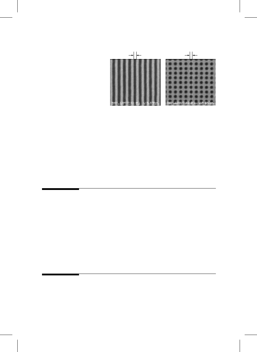
shows Ta patterns etched by ECR systems; 70-nm-wide patterns are clearly
formed.
© 2005 by Taylor & Francis Group.
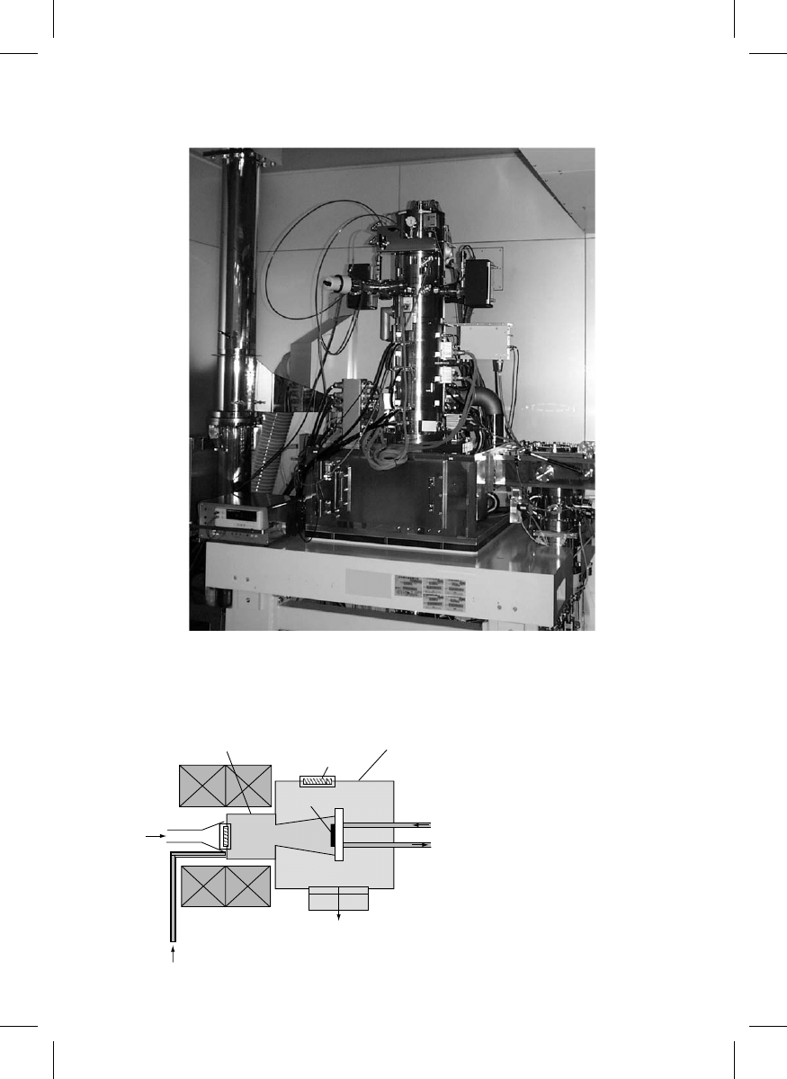
FIGURE 13.10
50-nm-wide resist patterns delineated by an EB writer with an acceleration voltage of 100 kV.
Plasma chamber
Etching chamber
View port
Microwaves
Sample
Chiller
Vacuum system
Magnet coils
Gas
ECR
Plasma
Ion stream
FIGURE 13.11
Schematic of the ECR ion stream
etching system.
© 2005 by Taylor & Francis Group.
13.3.4 Frame Bonding
The membrane can suffer deformation from frame bonding. There are two ways to
resolve this problem. One is to use a bonding method that does not deform the wafer.
For this purpose, the one-point bonding method [22] was developed. In this method, a
very small area of a wafer is bonded to a frame, and only that area contacts the frame
surface. This is useful for mask processes, in which bonding is the final step. The other
way is a process in which the bonding is done before patterning the absorber. In this
process, bonding must be very hard so that the wafer does not peel off during the
patterning process. Anodic bonding was developed for this purpose [23].
13.4
Defect Inspection and Repair
Defect inspection and repair are crucial to the production of x-ray masks for LSI processes.
A scanning electron beam system has been investigated for this purpose. For SiN or
diamond membrane, which is an insulator, it is difficult to inspect defects directly because
of the charge-up problem. Mask defects are therefore confirmed by inspecting wafers
having resist patterns replicating the mask patterns [24]. One can directly inspect defects
on SiC membrane because it has low conductivity. To repair defects in x-ray masks, a
focused-ion-beam repair system has been studied [25,26]. The system uses a Ga ion beam
focused to a spot less than 10 nm in diameter. Transparent defects are repaired by ion-
beam-induced deposition of Ta, and opaque defects are repaired by ion milling or gas-
assisted etching.
shows an example of a repair made to Ta absorber mask.
13.5
X-Ray Masks for LSI Fabrication
Many LSIs and devices have been produced using x-ray lithography. IBM developed x-
ray masks with 0.5-mm LSI patterns [27] and x-ray masks with 0.25-mm LSI patterns [28].
Mitsubishi Electric developed masks with 1-Gbit DRAM patterns in 1989 [29]. NEC
reported LSI masks in 1994 [30]. NTT developed x-ray masks with 200-nm [31] and 100-nm
[32] LSI patterns. NTT and Association of Super-Advanced Electronics Technologies
FIGURE 13.12
70-nm-wide Ta absorber patterns.
70 nm
67 nm
Lines and spaces
Holes
© 2005 by Taylor & Francis Group.
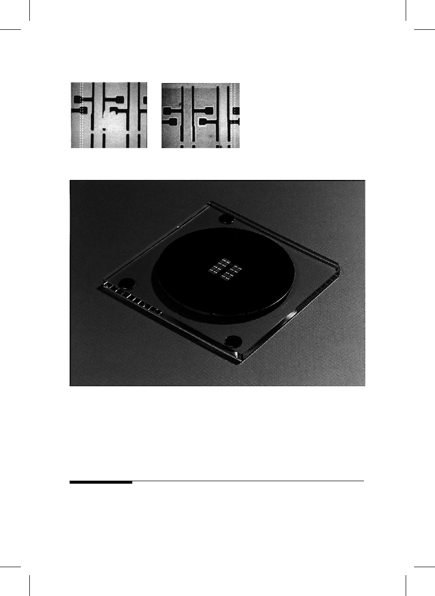
(ASET) developed masks with 100-nm LSI patterns with position accuracy of 25 nm in
1999 (Figure 13.14) [33]. The usefulness of x-ray lithography has been thoroughly proven
by these studies.
13.6
Summary
x-ray masks mainly consist of a thin membrane and absorber patterns. The membranes
are made of Si, SiN, SiC, or diamond film and Ta and W, or their compounds are used as
the absorbers. Stress control of these films is crucial in mask fabrication. An e-beam writer
(a) Before repair
(b) After repair
FIGURE 13.13
Ta absorber patterns repaired by a focused
ion-beam system.
FIGURE 13.14
X-ray mask.
Rizvi / Handbook of Photomask Manufacturing Technology DK2192_c013 Final Proof page 315 7.3.2005 6:25pm
© 2005 by Taylor & Francis Group.

with high acceleration voltage is necessary for pattern delineation on heavy metals.
Highly accurate masks can be fabricated by adopting a membrane process, in which
back-etching is carried out before the absorber film is patterned and then by correcting
any distortion. A scanning EB system and a focused-ion-beam system enable defect
inspection and repair. Highly accurate x-ray masks have been produced, and the useful-
ness of x-ray lithography has been proven.
References
1. D.L. Spears and H.I. Smith, High-resolution pattern replication using soft x-rays, Electron. Lett.,
8, 102–104 (1972).
2. R. Feder, E. Spiller, and J. Topalian, Replication of 0.1-mm geometries with x-ray lithography,
J. Vac. Sci. Technol., 12, 1332–1335 (1975).
3. T. Hosokawa, T. Kitayama, T. hayasaka, S. Ido, Y. Uno, A. Shibayama, J. Nakata, and
K. Nishimura, NTT superconducting storage ring—Super-ALIS, Rev. Sci. Instrum., 60, 1783–
1786 (1989).
4. M. Sekimoto, H. Yoshihara, and T. Ohkubo, Silicon nitride single-layer x-ray mask, J. Vac. Sci.
Technol., 21, 1017 (1982).
5. M. Yamada, M. Nakaishi, J. Kudou, T. Eshita, and Y. Furumura, An x-ray mask using Ta and
heteroepitaxially grown SiC, Microelectron. Eng., 88, 135–138 (1989).
6. H. Windischmann and G.F. Epps, Properties of diamond membranes for x-ray lithography,
J. Appl. Phys., 68, 5665–5673 (1990).
7. K. Yamashiro, M. Sugawara, H. Nagasawa, and Y. Yamaguchi, Smoothing roughness of SiC
membrane surface for x-ray masks, Jpn. J. Appl. Phys., 30, 3078–3082 (1991).
8. W.A. Johnson, R.A. Levy, D.J. Resnick, T.E. Saunders, A.W. Yanof, H. Betz, H. Huber, and
H. Oertel, Radiation damage effects in boron nitride mask membranes subjected to x-ray
exposures, J. Vac. Sci. Technol. B., 5, 257–261 (1987).
9. T. Kitayama, K. Itoga, Y. Watanabe, and S. Uzawa, Proposal for a 50 nm proximity x-ray
lithography system and extension to 35 nm by resist material selection, J. Vac. Sci. Technol. B.,
18, 2950–2954 (2000).
10. H.I. Smith, D.L. Spears, S.E. Bernacki, x-ray lithography: a complementary technique to electron
beam lithography, J. Vac. Sci. Technol., 10, 913–917 (1973).
11. H. Sekimoto, A. Ozawa, T. Ohkubo, and H. Yoshihara, A High Contrast Submicron x-ray Mask
with Ta Absorber Patterns, Extended Abstracts of the 16th (1984 International) Conference on
Solid State Devices and Materials, Kobe, 1984, pp. 23–26.
12. R.R. Kola, G.K. Celler, J. Frackoviak, C.W. Jurgensen, and L.E. Trimble, Stable low-stress
tungsten absorber technology for sub-half-micron x-ray lithography, J. Vac. Sci. Technol. B., 9,
3301–3304 (1991).
13. K. Marumoto, H. Yabe, S. Aya, K. Kise, and Y. Matsui, Total evaluation of W–Ti absorber for
X-ray mask, Proc. SPIE, 2194, 221–230 (1994).
14. S. Tsuboi, Y. Tanaka, T. Iwamoto, H. Sumitani, and Y. Nakayama, Recent progress in 1 x-ray
mask technology: feasibility study using ASET-NIST format TaXN x-ray masks with 100 nm
rule 4 Gbit dynamic random access memory test patterns, J. Vac. Sci. Technol. B., 19, 2416–2422
(2001).
15. M. Shimada, T. Tsuchizawa, S. Uchiyama, T. Ohkubo, S. Itabashi, I. Okada, T. Ono, and M. Oda,
Development of highly accurate x-ray mask with high-density patterns, Jpn. J. Appl. Phys., 38,
7071–7075 (1999).
16. S. Uchiyama, S. Ohki, A. Ozawa, M. Oda, T. Matsuda, and T. Morosawa, Improving x-ray mask
pattern placement accuracy by correcting process distortion in electron beam writing, Jpn.
J. Appl. Phys., 34, 6743–6747 (1995).
Rizvi / Handbook of Photomask Manufacturing Technology DK2192_c013 Final Proof page 316 7.3.2005 6:25pm
© 2005 by Taylor & Francis Group.

17. D. Pusito, M. Struns, and M. Lawliss, Overlay enhancement with product-specific emulation in
electron-beam lithography tools, J. Vac. Sci. Technol. B., 12, 3436–3439 (1994).
18. M. Oda, M. Shimada, T. Tsuchizawa, S. Uchiyama, I. Okada, and H. Yoshihara, Progress in
x-ray mask technology at NTT, J. Vac. Sci. Technol. B., 17, 3402–3406 (1999).
19. S. Ohki, T. Watanabe, Y. Takeda, T. Morosawa, K. Saito, T. Kunioka, J. Kato, A. Shimizu,
T. Matsuda, S. Tsuboi, H. Aoyama, H. Watanabe, and Y. Nakayama, Patterning performance
of EB-X3 x-ray mask writer, J. Vac. Sci. Technol. B., 18, 3084–3088 (2000).
20. K.K. Christenson, R.G. Viswanathan, and F.J. Hohn, x-ray mask fogging by electrons back-
scattered beneath the membrane, J. Vac. Sci. Technol. B., 8, 1618–1623 (1990).
21. T. Tsuchizawa, H. Iriguchi, C. Takahashi, M. Shimada, S. Uchiyama, and M. Oda, Electron
cyclotron resonance plasma etching of a-Ta for x-ray mask absorber using chlorine and fluoride
gas mixture, Jpn. J. Appl. Phys., 39, 6914–6918 (2000).
22. M. Oda, T. Ohkubo, and H. Yoshihara, One-point wafer bonding for highly accurate x-ray
masks, Proc. SPIE, 2512, 152–159 (1995).
23. J. Trube, J. Chlebek, J. Grimm, H.-L. Huber, B. Lochel, and H. Stauch, Investigation of process
latitude for quality improvement in x-ray lithography mask fabrication, J. Vac. Sci. Technol. B., 8,
1600–1603 (1990).
24. M. Sekimoto, H. Tsuyozaki, I. Okada, A. Shibayama, and T. Matsuda, x-ray mask inspection
using replicated resist patterns, Jpn. J. Appl. Phys., 33, 6913–6918 (1994).
25. I. Okada, Y. Saitoh, T. Ohkubo, M. Sekimoto, and T. Matsuda, Repairing x-ray masks with Ta
absorbers using focused ion beams, Proc. SPIE, 2512, 172–177 (1995).
26. A. Wangner, J.P. Levin, J.L. Maner, P.G. Blauner, S.J. Kirch, and P. Longo, x-ray mask repair
with focused ion beams, J. Vac. Sci. Technol. B., 8, 1557–1564 (1990).
27. R. Viswanathan, R.E. Acosta, D. Seeger, H. Voelker, A. Wilson, I. Babich, J. Maldonado,
J. Warlaumont, O. Vladimirsky, F. Hohn, D. Crockatt, and R. Fair, Fully scaled 0.5 mm metal–
oxide semiconductor circuits by synchrotron x-ray lithography: mask fabrication and charac-
terization, J. Vac. Sci. Technol. B., 6, 2196–2201 (1988).
28. R. Viswanathan, D. Seeger, A. Bright, T. Bucelot, A. Pomerene, K. Petrillo, P. Blauner, P. Agnello,
J. Warlaumont, J. Conway, and D. Patel, Fabrication of high performance 512Kb SRAMs in
0.25 mm CMOS technology using x-ray lithography, Microelectron. Eng., 23, 247–252 (1994).
29. N. Yoshioka, N. Ishio, N. Fujiwara, T. Eimori, Y. Watakabe, K. Kodama, T. Miyachi, and
H. Izawa, Fabrication of 1-Mbit DRAMs by using x-ray lithography, Proc. SPIE, 1089, 210–218
(1989).
30. K. Fujii, T. Yoshihara, Y. Tanaka, K. Suzuki, T. Nakajima, T. Miyatake, E. Orita, and K. Ito,
Applicability test for synchrotron radiation x-ray lithography in 64-Mb dynamic random access
memory fabrication processes, J. Vac. Sci. Technol. B., 12, 3949–3953 (1994).
31. K. Deguchi, K. Miyoshi, H. Ban, T. Matsuda, T. Ohno, and Y. Kado, Fabrication of 0.2 mm large
scale integrated circuits using synchrotron radiation x-ray lithography, J. Vac. Sci. Technol. B., 13,
3040–3045 (1995).
32. M. Oda, S. Uchiyama, T. Watanabe, K. Komatsu, and T. Matsuda, x-ray mask fabrication
technology for 0.1 mm very large scale integrated circuits, J. Vac. Sci. Technol. B., 14, 4366–4370
(1996).
33. H. Aoyama, T. Taguchi, Y. Matsui, M. Fukuda, K. Deguchi, H. Morita, M. Oda, T. Matsuda,
F. Kumasaka, Y. Iba, and K. Horiuchi, Overlay evaluation of proximity x-ray lithography in
100 nm device fabrication, J. Vac. Sci. Technol. B., 18, 2961–2965 (2000).
© 2005 by Taylor & Francis Group.
Document Outline
- Contents
- Section IV NGL Masks
Wyszukiwarka
Podobne podstrony:
CH13
Ch13 Q4
cisco2 ch13 concept DEPLAEMNY56CXKYBER7D5JJA4Y4E4WS45RAVJSI
Ch13 Drawing Views
Ch13 Q3
CH13 2
Ch13 Q1
Ch13
ch13
Ch13 Q2
Ch13 Shafts
Genomes3e ppt ch13
ch13
Ch13 PolutionAndItsControll
Ch13 rolling
Ch13 Pg441 484
CH13
Ch13 Q4
więcej podobnych podstron