HCC/HCF4585B
June 1989
4-BIT MAGNITUDE COMPARATOR
.
EXPANSION TO 8, 12, 16 ... 4 N BITS BY CAS-
CADING UNITS
.
MEDIUM-SPEED OPERATION : COMPARES
TWO 4-BIT WORDS IN 180ns (typ.) AT 10V
.
STANDARDIZED
SYMMETRICAL
OUTPUT
CHARACTERISTICS
.
5V, 10V, AND 15V PARAMETRIC RATINGS
.
INPUT CURRENT OF 100nA AT 18V AND 25
°
C
FOR HCC DEVICE
.
100% TESTED FOR QUIESCENT CURRENT
.
MEETS ALL REQUIREMENTS OF JEDEC TEN-
TATIVE STANDARD N
°
13A, ”STANDARD SPE-
CIFICATIONS FOR DESCRIPTION OF ”B”
SERIES CMOS DEVICES”
DESCRIPTION
The HCC4585B (extended temperature range) and
HCF4585B (intermediate temperature range) are
monolithic integrated circuits, available in 16-lead
dual in-line plastic or ceramic package, and plastic
micro package. The HCC/HCF4585B is a 4-bit mag-
nitude comparator designed for use in computer and
logic applications that require the comparison of two
4-bit words. This logic circuit determines whether
one 4-bit word (Binary or BCD) is ”less than”, ”equal
to”, or ”greater than” a second 4-bit word. The
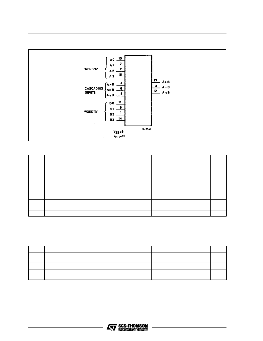
HCC/HCF4585B has eight comparing inputs (A3,
B3, through A0, B0), three outputs (A < B, A = B, A >
B) and three cascading inputs (A < B, A = B, A > B)
that permit systems designers to expand the com-
parator function to 8, 12, 16 ... 4 N bits. When a
single HCC/HCF4585B is used, the cascading in-
puts are connected as follows : (A < B) = low,
(A = B) = high, (A > B) = high. Cascading these units
for comparison of more than 4 bits is accomplished
as shown in typical application.
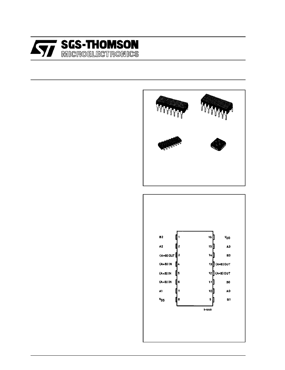
EY
(Plastic Package)
F
(Ceramic Frit Seal Package)
C1
(Plastic Chip Carrier)
ORDER CODES :
HCC4585BF
HCF4585BM1
HCF4585BEY
HCF4585BC1
PIN CONNECTIONS
M1
(Micro Package)
1/12
ABSOLUTE MAXIMUM RATINGS
Symbol
Parameter
Value
Unit
V
DD
*
Supply Voltage : HC C Types
H C F Types
– 0.5 to + 20
– 0.5 to + 18
V
V
V
i
Input Voltage
– 0.5 to V
DD
+ 0.5
V
I
I
DC Input Current (any one input)
±
10
mA
P
t o t
Total Power Dissipation (per package)
Dissipation per Output Transistor
for T
o p
= Full Package-temperature Range
200
100
mW
mW
T
o p
Operating Temperature : HCC Types
H CF Types
– 55 to + 125
– 40 to + 85
°
C
°
C
T
s t g
Storage Temperature
– 65 to + 150
°
C
Stresses above those listed under ”Absolute Maximum Ratings” may cause permanent damage to the device. This is a stress
rating only and functional operation of the device at these or any other conditions above those indicated in the operational sections
of this specification is not implied. Exposure to absolute maximum rating conditions for external periods may affect device reliability.
* All voltages are with respect to V
SS
(GND).
FUNCTIONAL DIAGRAM
RECOMMENDED OPERATING CONDITIONS
Symbol
Parameter
Value
Unit
V
DD
Supply Voltage : H CC Types
H C F Types
3 to 18
3 to 15
V
V
V
I
Input Voltage
0 to V
DD
V
T
o p
Operating Temperature : HCC Types
H CF Types
– 55 to + 125
– 40 to + 85
°
C
°
C
HCC/HCF4585B
2/12
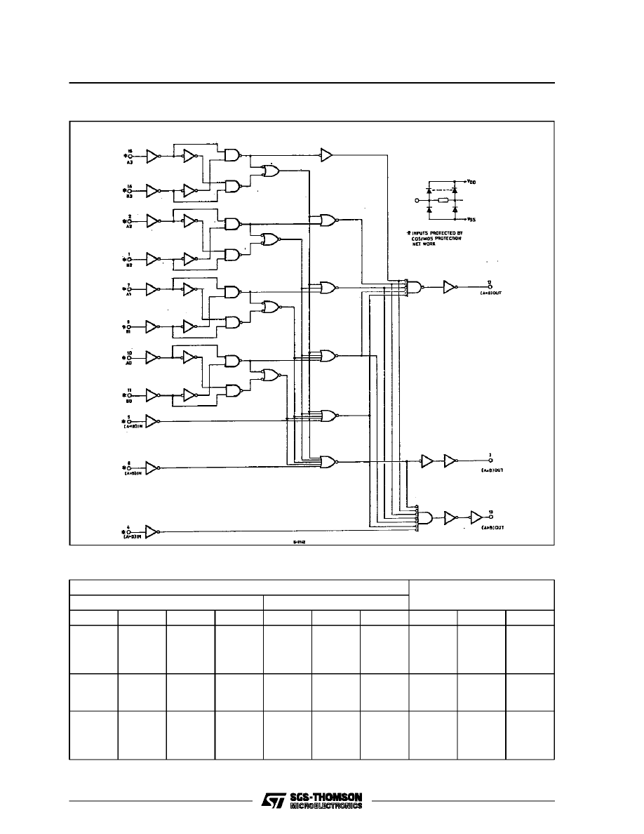
LOGIC DIAGRAM
Inputs
Compari ng
Cascading
Outputs
A 3 , B 3
A 2 , B 2 A 1 , B 1
A 0 , B 0
A < B
A = B
A > B
A < B
A = B
A > B
A3 > B3
A3 = B3
A3 = B3
A3 = B3
X
A2 > B2
A2 = B2
A2 = B2
X
X
A1 > B1
A1 = B1
X
X
X
A0 > B0
X
X
X
X
X
X
X
X
1
1
1
1
0
0
0
0
0
0
0
0
1
1
1
1
A3 = B3
A3 = B3
A3 = B3
A2 = B2
A2 = B2
A2 = B2
A1 = B1
A1 = B1
A1 = B1
A0 = B0
A0 = B0
A0 = B0
0
0
1
0
1
0
1
X
X
0
0
1
0
1
0
1
0
0
A3 = B3
A3 = B3
A3 = B3
A3 < B3
A2 = B2
A2 = B2
A2 < B2
X
A1 = B1
A1 < B1
X
X
A0 < B0
X
X
X
X
X
X
X
X
X
X
X
X
X
X
X
1
1
1
1
0
0
0
0
0
0
0
0
X = Don’t Care
Logic 1 = High Level
TRUTH TABLE
HCC/HCF4585B
3/12
STATIC ELECTRICAL CHARACTERISTICS (over recommended operating conditions)
Test Conditions
Value
V
I
V
O
|I
O
|
V
D D
T
L o w
*
25
°
C
T
Hi g h
*
Symbol
Parameter
(V)
(V)
(
µ
A)
(V)
Min. Max. Min. Typ. Max. Min. Max.
Unit
I
L
Quiescent
Current
HCC
Types
0/ 5
5
5
0.04
5
150
µ
A
0/10
10
10
0.04
10
300
0/15
15
20
0.04
20
600
0/20
20
100
0.08
100
3000
HCF
Types
0/ 5
5
20
0.04
20
150
0/10
10
40
0.04
40
300
0/15
15
80
0.04
80
600
V
O H
Output High
Voltage
0/ 5
< 1
5
4.95
4.95
4.95
V
0/10
< 1
10
9.95
9.95
9.95
0/15
< 1
15
14.95
14.95
14.95
V
O L
Output Low
Voltage
5/0
< 1
5
0.05
0.05
0.05
V
10/0
< 1
10
0.05
0.05
0.05
15/0
< 1
15
0.05
0.05
0.05
V
IH
Input High
Voltage
0.5/4.5
< 1
5
3.5
3.5
3.5
V
1/9
< 1
10
7
7
7
1.5/13.5
< 1
15
11
11
11
V
IL
Input Low
Voltage
4.5/0.5
< 1
5
1.5
1.5
1.5
V
9/1
< 1
10
3
3
3
13.5/1.5
< 1
15
4
4
4
I
O H
Output
Drive
Current
HCC
Types
0/ 5
2.5
5
– 2
– 1.6 – 3.2
– 1.15
mA
0/ 5
4.6
5
– 0.64
– 0.51 – 1
– 0.36
0/10
9.5
10
– 1.6
– 1.3 – 2.6
– 0.9
0/15
13.5
15
– 4.2
– 3.4 – 6.8
– 2.4
HCF
Types
0/ 5
2.5
5
– 1.53
– 1.36 – 3.2
– 1.1
0/ 5
4.6
5
– 0.52
– 0.44 – 1
– 0.36
0/10
9.5
10
– 1.3
– 1.1 – 2.6
– 0.9
0/15
13.5
15
– 3.6
– 3.0 – 6.8
– 2.4
I
O L
Output
Sink
Current
HCC
Types
0/ 5
0.4
5
0.64
0.51
1
0.36
mA
0/10
0.5
10
1.6
1.3
2.6
0.9
0/15
1.5
15
4.2
3.4
6.8
2.4
HCF
Types
0/ 5
0.4
5
0.52
0.44
1
0.36
0/10
0.5
10
1.3
1.1
2.6
0.9
0/15
1.5
15
3.6
3.0
6.8
2.4
I
IH
, I
IL
Input
Leakage
Current
HCC
Types
0/18
Any Input
18
±
0.1
±
10
– 5
±
0.1
±
1
µ
A
HCF
Types
0/15
15
±
0.3
±
10
– 5
±
0.3
±
1
C
I
Input Capacitance
Any Input
5
7.5
pF
* T
Lo w
= – 55
°
C for HCC device : – 40
°
C for HCF device.
* T
High
= + 125
°
C for HCC device : + 85
°
C for HCF device.
The Noise Margin for both ”1” and ” 0” level is : 1V min. with V
DD
= 5V, 2V min. with V
DD
= 10V, 2.5V min. with V
DD
= 15V.
HCC/HCF4585B
4/12
DYNAMIC ELECTRICAL CHARACTERISTICS (T
amb
= 25
°
C, C
L
= 50pF, R
L
= 200k
Ω
,
typical temperature coefficient for all V
DD
values is 0.3%/
°
C, all input rise and fall time = 20ns)
Test Conditions
Val ue
Symbol
Parameter
V
D D
(V)
Min.
Typ.
Max.
Unit
t
PHL
,
t
P L H
Propagation Delay Time
Comparing Inputs to Outputs
5
300
600
ns
10
125
250
15
80
160
Cascading Input to Outputs
5
200
400
ns
10
80
160
15
60
120
t
T HL
,
t
T L H
Transition Time
5
100
200
ns
10
50
100
15
40
80
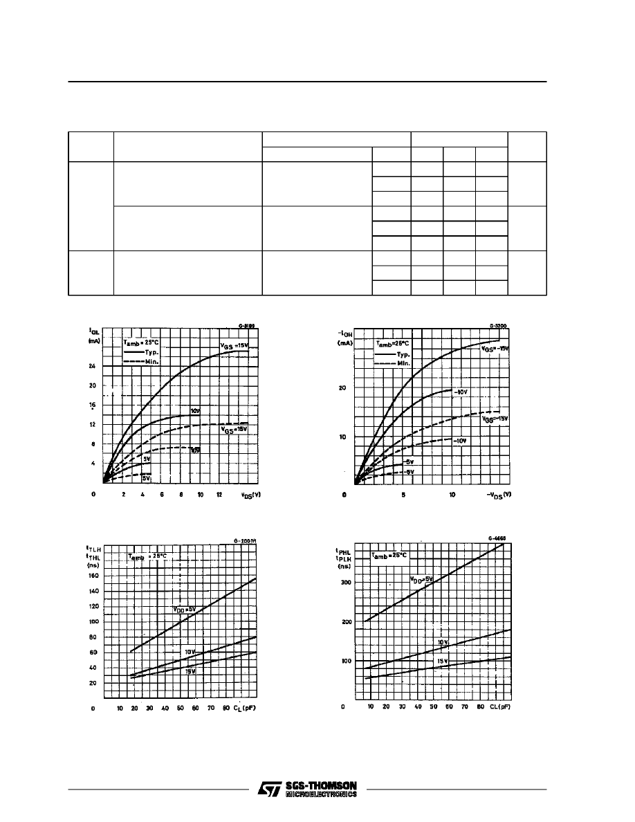
Output Low (sink) Current Characteristics.
Output High (source) Current Characteristics.
Typical Transition Time vs. Load Capacitance.
Typical Propagation Delay Time (comparing in-
puts to outputs) vs. Load Capacitance.
HCC/HCF4585B
5/12
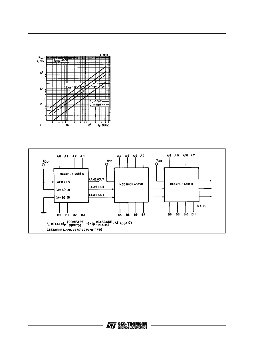
TYPICAL APPLICATION
TYPICAL SPEED CHARACTERISTICS OF A 12-BIT COMPARATOR
Typical Dynamic Power Dissipation vs. Clock
Input Frequency.
HCC/HCF4585B
6/12

TEST CIRCUITS
Quiescent Device Current.
Input Voltage.
Input Leakage Current.
Dynamic Power Dissipation.
HCC/HCF4585B
7/12
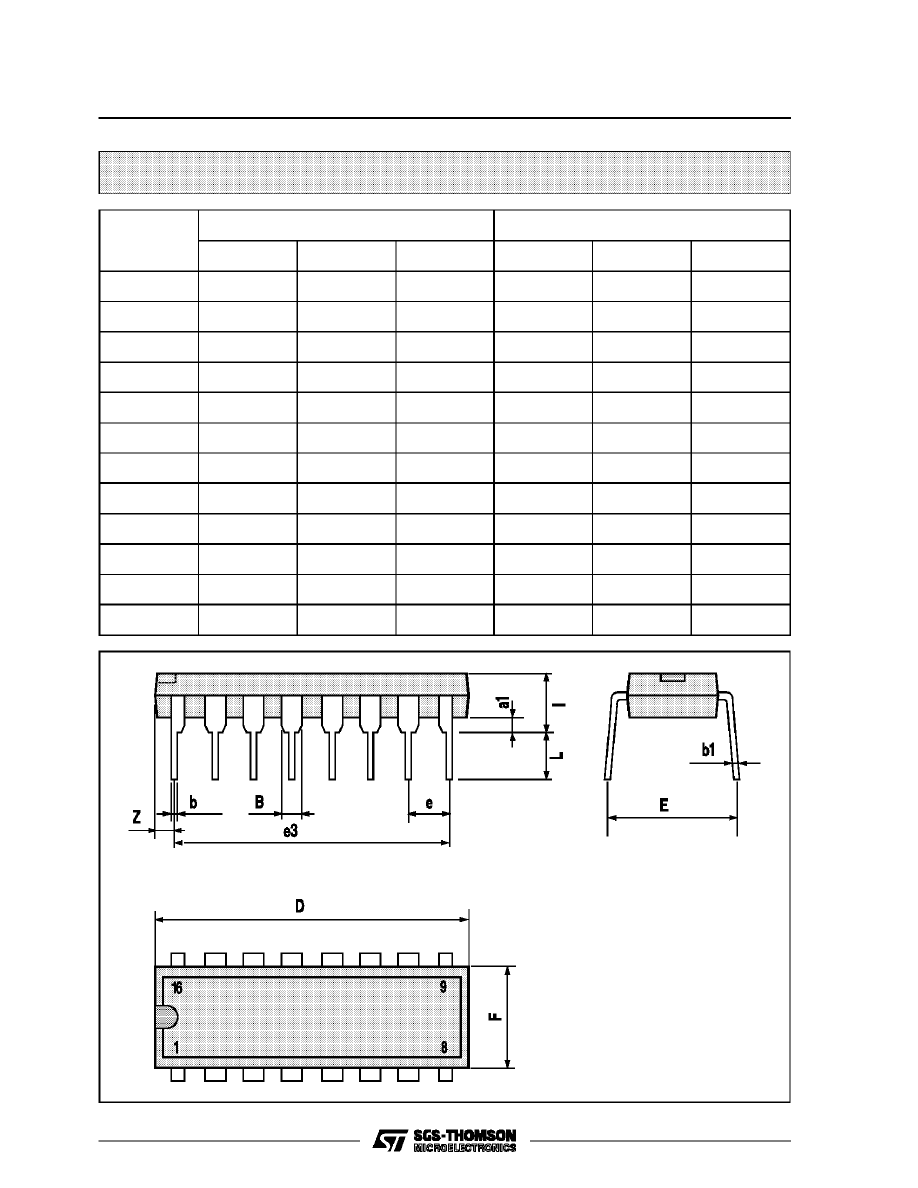
Plastic DIP16 (0.25) MECHANICAL DATA
DIM.
mm
inch
MIN.
TYP.
MAX.
MIN.
TYP.
MAX.
a1
0.51
0.020
B
0.77
1.65
0.030
0.065
b
0.5
0.020
b1
0.25
0.010
D
20
0.787
E
8.5
0.335
e
2.54
0.100
e3
17.78
0.700
F
7.1
0.280
I
5.1
0.201
L
3.3
0.130
Z
1.27
0.050
P001C
HCC/HCF4585B
8/12

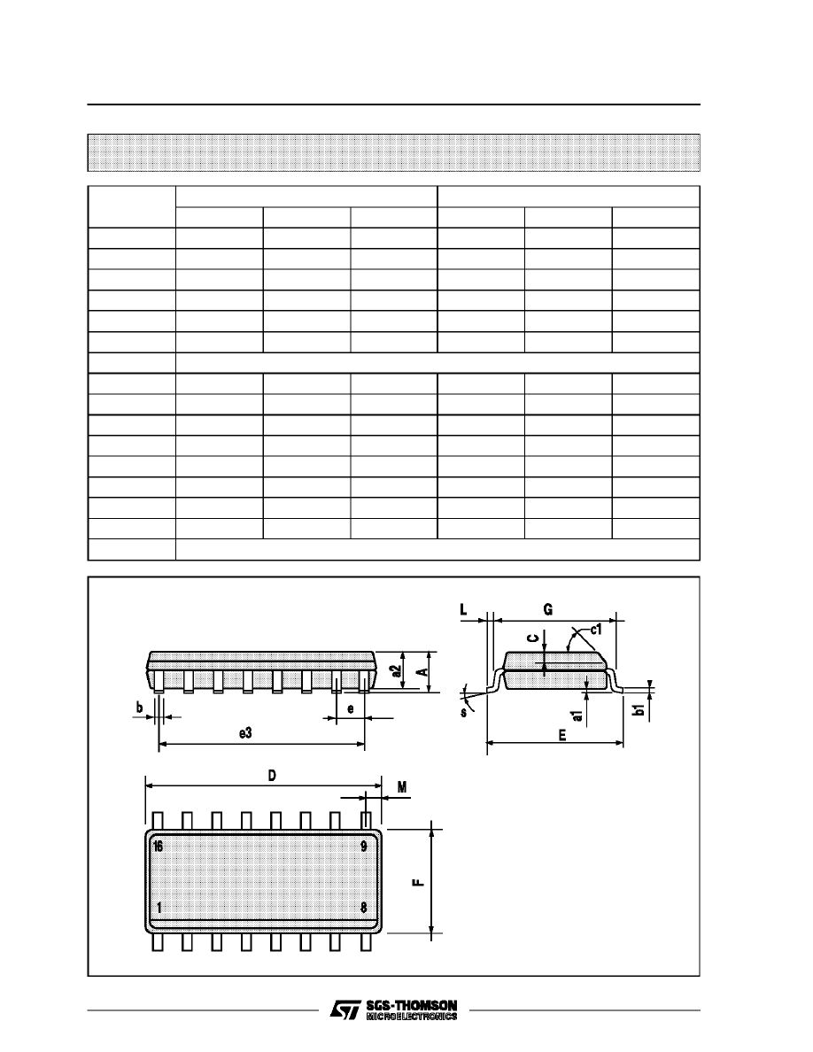
Ceramic DIP16/1 MECHANICAL DATA
DIM.
mm
inch
MIN.
TYP.
MAX.
MIN.
TYP.
MAX.
A
20
0.787
B
7
0.276
D
3.3
0.130
E
0.38
0.015
e3
17.78
0.700
F
2.29
2.79
0.090
0.110
G
0.4
0.55
0.016
0.022
H
1.17
1.52
0.046
0.060
L
0.22
0.31
0.009
0.012
M
0.51
1.27
0.020
0.050
N
10.3
0.406
P
7.8
8.05
0.307
0.317
Q
5.08
0.200
P053D
HCC/HCF4585B
9/12
SO16 (Narrow) MECHANICAL DATA
DIM.
mm
inch
MIN.
TYP.
MAX.
MIN.
TYP.
MAX.
A
1.75
0.068
a1
0.1
0.2
0.004
0.007
a2
1.65
0.064
b
0.35
0.46
0.013
0.018
b1
0.19
0.25
0.007
0.010
C
0.5
0.019
c1
45
°
(typ.)
D
9.8
10
0.385
0.393
E
5.8
6.2
0.228
0.244
e
1.27
0.050
e3
8.89
0.350
F
3.8
4.0
0.149
0.157
G
4.6
5.3
0.181
0.208
L
0.5
1.27
0.019
0.050
M
0.62
0.024
S
8
°
(max.)
P013H
HCC/HCF4585B
10/12
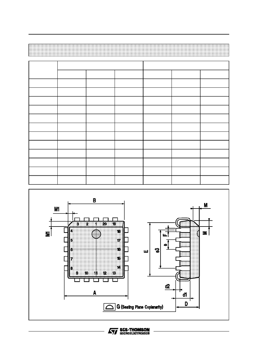
PLCC20 MECHANICAL DATA
DIM.
mm
inch
MIN.
TYP.
MAX.
MIN.
TYP.
MAX.
A
9.78
10.03
0.385
0.395
B
8.89
9.04
0.350
0.356
D
4.2
4.57
0.165
0.180
d1
2.54
0.100
d2
0.56
0.022
E
7.37
8.38
0.290
0.330
e
1.27
0.050
e3
5.08
0.200
F
0.38
0.015
G
0.101
0.004
M
1.27
0.050
M1
1.14
0.045
P027A
HCC/HCF4585B
11/12

Information furnished is believed to be accurate and reliable. However, SGS-THOMSON Microelectronics assumes no responsability for the
consequences of use of such information nor for any infringement of patents or other rights of third parties which may results from its use. No
license is granted by implication or otherwise under any patent or patent rights of SGS-THOMSON Microelectronics. Specifications mentioned
in this publication are subject to change without notice. This publication supersedes and replaces all information previously supplied.
SGS-THOMSON Microelectronics products are not authorized for use as critical components in life support devices or systems without express
written approval of SGS-THOMSON Microelectonics.
1994 SGS-THOMSON Microelectronics - All Rights Reserved
SGS-THOMSON Microelectronics GROUP OF COMPANIES
Australia - Brazil - France - Germany - Hong Kong - Italy - Japan - Korea - Malaysia - Malta - Morocco - The Netherlands -
Singapore - Spain - Sweden - Switzerland - Taiwan - Thailand - United Kingdom - U.S.A
HCC/HCF4585B
12/12
Wyszukiwarka
Podobne podstrony:
4585
03 A 2 Deck Linesid 4585
4585
praca-licencjacka-b7-4585, Dokumenty(8)
4585
4585, W3 - chemiczny
4585
4585
4585
IMSLP87936 SIBLEY1802 4585 d270 39087012433308Murschhauser
adamantyl cannabinoids a novel class of cannabinergic ligands j med chem 48 4576 4585 (2005)
więcej podobnych podstron