TIP100, TIP101, TIP102
NPN SILICON POWER DARLINGTONS
1
AUGUST 1978 - REVISED SEPTEMBER 2002
Specifications are subject to change without notice.
●
Designed for Complementary Use with
TIP105, TIP106 and TIP107
●
80 W at 25°C Case Temperature
●
8 A Continuous Collector Current
●
Maximum V
CE(sat)
of 2.5 V at I
C
= 8 A
absolute maximum ratings at 25°C case temperature (unless otherwise noted)
NOTES: 1. This value applies for t
p
≤ 0.3 ms, duty cycle ≤ 10%.
2. Derate linearly to 150°C case temperature at the rate of 0.64 W/°C.
3. Derate linearly to 150°C free air temperature at the rate of 16 mW/°C.
4. This rating is based on the capability of the transistor to operate safely in a circuit of: L = 20 mH, I
B(on)
= 5 mA, R
BE
= 100
Ω,
V
BE(off)
= 0, R
S
= 0.1
Ω, V
CC
= 20 V.
RATING
SYMBOL
VALUE
UNIT
Collector-base voltage (I
E
= 0)
TIP100
TIP101
TIP102
V
CBO
60
80
100
V
Collector-emitter voltage (I
B
= 0)
TIP100
TIP101
TIP102
V
CEO
60
80
100
V
Emitter-base voltage
V
EBO
5
V
Continuous collector current
I
C
8
A
Peak collector current (see Note 1)
I
CM
15
A
Continuous base current
I
B
1
A
Continuous device dissipation at (or below) 25°C case temperature (see Note 2)
P
tot
80
W
Continuous device dissipation at (or below) 25°C free air temperature (see Note 3)
P
tot
2
W
Unclamped inductive load energy (see Note 4)
½LI
C
2
10
mJ
Operating junction temperature range
T
j
-65 to +150
°C
Storage temperature range
T
stg
-65 to +150
°C
Lead temperature 3.2 mm from case for 10 seconds
T
L
260
°C
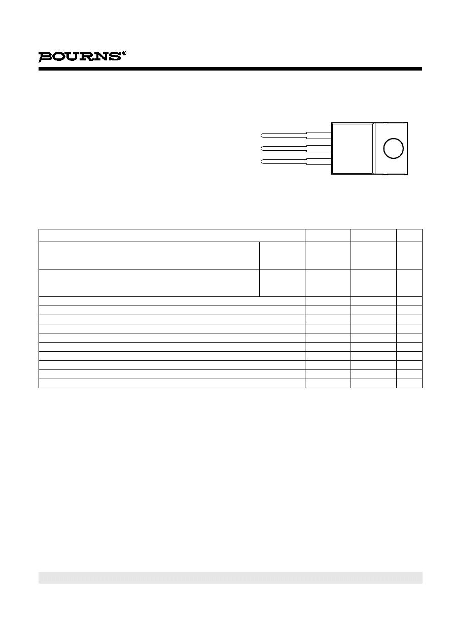
B
C
E
TO-220 PACKAGE
(TOP VIEW)
Pin 2 is in electrical contact with the mounting base.
MDTRACA
1
2
3
TIP100, TIP101, TIP102
NPN SILICON POWER DARLINGTONS
2
AUGUST 1978 - REVISED SEPTEMBER 2002
Specifications are subject to change without notice.
NOTES: 5. These parameters must be measured using pulse techniques, t
p
= 300 µs, duty cycle
≤ 2%.
6. These parameters must be measured using voltage-sensing contacts, separate from the current carrying contacts.
†
Voltage and current values shown are nominal; exact values vary slightly with transistor parameters.
electrical characteristics at 25°C case temperature
PARAMETER
TEST CONDITIONS
MIN
TYP
MAX
UNIT
V
(BR)CEO
Collector-emitter
breakdown voltage
I
C
= 30 mA
(see Note 5)
I
B
= 0
TIP100
TIP101
TIP102
60
80
100
V
I
CEO
Collector-emitter
cut-off current
V
CE
= 30 V
V
CE
= 40 V
V
CE
= 50 V
I
B
= 0
I
B
= 0
I
B
= 0
TIP100
TIP101
TIP102
50
50
50
µA
I
CBO
Collector cut-off
current
V
CB
= 60 V
V
CB
= 80 V
V
CB
= 100 V
I
E
= 0
I
E
= 0
I
E
= 0
TIP100
TIP101
TIP102
50
50
50
µA
I
EBO
Emitter cut-off
current
V
EB
= 5 V
I
C
= 0
8
mA
h
FE
Forward current
transfer ratio
V
CE
= 4 V
V
CE
= 4 V
I
C
= 3 A
I
C
= 8 A
(see Notes 5 and 6)
1000
200
20000
V
CE(sat)
Collector-emitter
saturation voltage
I
B
= 6 mA
I
B
= 80 mA
I
C
= 3 A
I
C
= 8 A
(see Notes 5 and 6)
2
2.5
V
V
BE
Base-emitter
voltage
V
CE
= 4 V
I
C
= 8 A
(see Notes 5 and 6)
2.8
V
V
EC
Parallel diode
forward voltage
I
E
= 8 A
I
B
= 0
(see Notes 5 and 6)
3.5
V
thermal characteristics
PARAMETER
MIN
TYP
MAX
UNIT
R
θJC
Junction to case thermal resistance
1.56
°C/W
R
θJA
Junction to free air thermal resistance
62.5
°C/W
C
θC
Thermal capacitance of case
0.9
J/°C
resistive-load-switching characteristics at 25°C case temperature
PARAMETER
TEST CONDITIONS
†
MIN
TYP
MAX
UNIT
t
d
Delay time
I
C
= 8 A
V
BE(off)
= -5 V
I
B(on)
= 80 mA
R
L
= 5
Ω
I
B(off)
= -80 mA
t
p
= 20 µs, dc
≤ 2%
35
ns
t
r
Rise time
350
ns
t
s
Storage time
1.8
µs
t
f
Fall time
2.45
µs
TIP100, TIP101, TIP102
NPN SILICON POWER DARLINGTONS
3
AUGUST 1978 - REVISED SEPTEMBER 2002
Specifications are subject to change without notice.
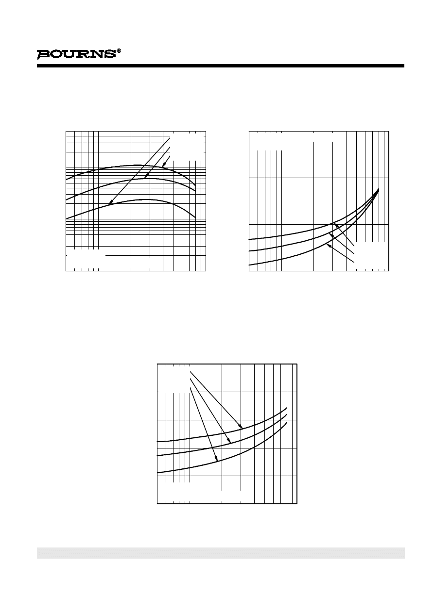
TYPICAL CHARACTERISTICS
Figure 1.
Figure 2.
Figure 3.
TYPICAL DC CURRENT GAIN
vs
COLLECTOR CURRENT
I
C
- Collector Current - A
0·5
1·0
10
h
FE
-
T
y
pi
c
a
l
D
C
Cu
rr
e
n
t
G
a
in
50000
100
1000
10000
TCS130AA
T
C
= -40°C
T
C
= 25°C
T
C
= 100°C
V
CE
= 4 V
t
p
= 300 µs, duty cycle < 2%
COLLECTOR-EMITTER SATURATION VOLTAGE
vs
COLLECTOR CURRENT
I
C
- Collector Current - A
0·5
1·0
10
V
C
E
(sat
)
- Co
ll
e
c
to
r-Em
itte
r Sa
tu
ra
ti
o
n
Vo
lt
a
g
e
- V
0·5
1·0
1·5
2·0
TCS130AB
T
C
= -40°C
T
C
= 25°C
T
C
= 100°C
t
p
= 300 µs, duty cycle < 2%
I
B
= I
C
/ 100
BASE-EMITTER SATURATION VOLTAGE
vs
COLLECTOR CURRENT
I
C
- Collector Current - A
0·5
1·0
10
V
B
E
(sat
)
- Ba
s
e
-E
m
itte
r Sa
tu
ra
ti
o
n
Vo
lt
a
g
e
- V
0·5
1·0
1·5
2·0
2·5
3·0
TCS130AC
T
C
= -40°C
T
C
= 25°C
T
C
= 100°C
I
B
= I
C
/ 100
t
p
= 300 µs, duty cycle < 2%
TIP100, TIP101, TIP102
NPN SILICON POWER DARLINGTONS
4
AUGUST 1978 - REVISED SEPTEMBER 2002
Specifications are subject to change without notice.
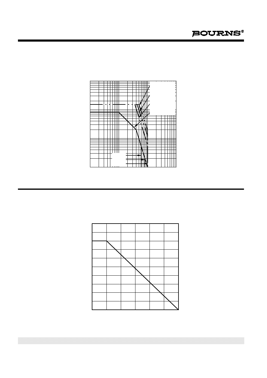
MAXIMUM SAFE OPERATING REGIONS
Figure 4.
THERMAL INFORMATION
Figure 5.
MAXIMUM FORWARD-BIAS
SAFE OPERATING AREA
V
CE
- Collector-Emitter Voltage - V
1·0
10
100
1000
I
C
- Co
ll
e
c
to
r Cu
rre
n
t
- A
0·1
1·0
10
100
SAS130AA
TIP100
TIP101
TIP102
t
p
= 100 µs,
d = 0.1 = 10%
t
p
= 1 ms,
d = 0.1 = 10%
t
p
= 5 ms,
d = 0.1 = 10%
DC Operation
MAXIMUM POWER DISSIPATION
vs
CASE TEMPERATURE
T
C
- Case Temperature - °C
0
25
50
75
100
125
150
P
to
t
-
M
a
x
im
u
m
P
o
w
e
r D
iss
ip
at
io
n
-
W
0
20
40
60
80
100
TIS130AA
Wyszukiwarka
Podobne podstrony:
TIP100, TIP101, TIP102 (Fairchild Semiconductor)
TIP125, TIP126, TIP127 (Bourns)
TIP100
TIP150, TIP151, TIP152 (Bourns)
TIP102, TIP107 (STMicroelectronics)
TIP130, TIP131, TIP132 (Bourns)
TIP30 (Bourns)
TIP102 105 107
TIP29 (Bourns)
więcej podobnych podstron