TIP150, TIP151, TIP152
NPN SILICON POWER DARLINGTONS
1
JUNE 1973 - REVISED SEPTEMBER 2002
Specifications are subject to change without notice.
●
80 W at 25°C Case Temperature
●
7 A Continuous Collector Current
●
10 A Peak Collector Current
●
Maximum V
CE(sat)
of 2 V at I
C
= 5 A
●
I
CEX(sus)
7 A at rated V
(BR)CEO
absolute maximum ratings at 25°C case temperature (unless otherwise noted)
NOTES: 1. This value applies for t
p
≤ 5 ms, duty cycle ≤ 10%.
2. Derate linearly to 150°C case temperature at the rate of 0.64 W/°C.
3. Derate linearly to 150°C free air temperature at the rate of 16 mW/°C.
RATING
SYMBOL
VALUE
UNIT
Collector-base voltage (I
E
= 0)
TIP150
TIP151
TIP152
V
CBO
300
350
400
V
Collector-emitter voltage (I
B
= 0)
TIP150
TIP151
TIP152
V
CEO
300
350
400
V
Emitter-base voltage
V
EBO
8
V
Continuous collector current
I
C
7
A
Peak collector current (see Note 1)
I
CM
10
A
Continuous base current
I
B
1.5
A
Continuous device dissipation at (or below) 25°C case temperature (see Note 2)
P
tot
80
W
Continuous device dissipation at (or below) 25°C free air temperature (see Note 3)
P
tot
2
W
Operating junction temperature range
T
j
-65 to +150
°C
Storage temperature range
T
stg
-65 to +150
°C
Lead temperature 3.2 mm from case for 10 seconds
T
L
260
°C
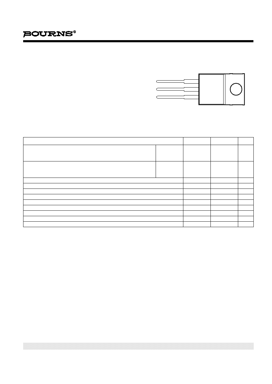
B
C
E
TO-220 PACKAGE
(TOP VIEW)
Pin 2 is in electrical contact with the mounting base.
MDTRACA
1
2
3
TIP150, TIP151, TIP152
NPN SILICON POWER DARLINGTONS
2
JUNE 1973 - REVISED SEPTEMBER 2002
Specifications are subject to change without notice.
NOTES: 4. These parameters must be measured using pulse techniques, t
p
= 300 µs, duty cycle
≤ 2%.
5. These parameters must be measured using voltage-sensing contacts, separate from the current carrying contacts.
†
Voltage and current values shown are nominal; exact values vary slightly with transistor parameters.
electrical characteristics at 25°C case temperature
PARAMETER
TEST CONDITIONS
MIN
TYP
MAX
UNIT
V
(BR)CBO
Collector-base
breakdown voltage
I
C
= 1 mA
I
E
= 0
TIP150
TIP151
TIP152
300
350
400
V
V
(BR)CEO
Collector-emitter
breakdown voltage
I
C
= 10 mA
(see Note 4)
I
B
= 0
TIP150
TIP151
TIP152
300
350
400
V
I
CEO
Collector-emitter
cut-off current
V
CE
= 300 V
V
CE
= 350 V
V
CE
= 400 V
I
B
= 0
I
B
= 0
I
B
= 0
TIP150
TIP151
TIP152
250
250
250
µA
I
CEX(sus)
Collector-emitter
sustaining current
V
CLAMP
= V
(BR)CEO
7
A
I
EBO
Emitter cut-off
current
V
EB
= 8 V
I
C
= 0
15
mA
h
FE
Forward current
transfer ratio
V
CE
= 5 V
V
CE
= 5 V
V
CE
= 5 V
I
C
= 2.5 A
I
C
= 5A
I
C
= 7 A
(see Notes 4 and 5)
150
50
15
V
CE(sat)
Collector-emitter
saturation voltage
I
B
= 10 mA
I
B
= 100 mA
I
B
= 250 mA
I
C
= 1 A
I
C
= 2 A
I
C
= 5 A
(see Notes 4 and 5)
1.5
1.5
2
V
V
BE(sat)
Base-emitter
saturation voltage
I
B
= 100 mA
I
B
= 250 mA
I
C
= 2 A
I
C
= 5 A
(see Notes 4 and 5)
2.2
2.3
V
V
EC
Parallel diode
forward voltage
I
E
= 7 A
I
B
= 0
(see Notes 4 and 5)
3.5
V
h
fe
Small signal forward
current transfer ratio
V
CE
= 5 V
I
C
= 0.5 A
f = 1 kHz
200
|
h
fe
|
Small signal forward
current transfer ratio
V
CE
= 5 V
I
C
= 0.5 A
f = 1 MHz
10
C
ob
Output capacitance
V
CB
= 10 V
I
E
= 0
f = 1 MHz
100
pF
thermal characteristics
PARAMETER
MIN
TYP
MAX
UNIT
R
θJC
Junction to case thermal resistance
1.56
°C/W
R
θJA
Junction to free air thermal resistance
62.5
°C/W
C
θC
Thermal capacitance of case
0.9
J/°C
inductive-load-switching characteristics at 25°C case temperature
PARAMETER
TEST CONDITIONS
†
MIN
TYP
MAX
UNIT
t
sv
Voltage storage time
I
C
= 5 A
V
(clamp)
= V
(BR)CEO
I
B(on)
= 250 mA
R
BE
= 47
Ω
3.9
µs
t
si
Current storage time
4.7
µs
t
rv
Voltage transition time
1.2
µs
t
ti
Current transition time
1.2
µs
t
xo
Cross-over time
2.0
µs
TIP150, TIP151, TIP152
NPN SILICON POWER DARLINGTONS
3
JUNE 1973 - REVISED SEPTEMBER 2002
Specifications are subject to change without notice.
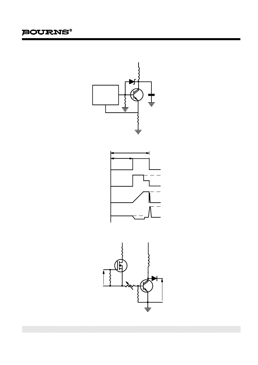
PARAMETER MEASUREMENT INFORMATION
Figure 1. Functional Test Circuit
Figure 2. Functional Test Waveforms
Figure 3. Switching Test Circuit
Driver and
Current
Limiting
Circuit
0.22
µF
V z
24 V
L = 7 mH
100
Ω
0.2
Ω
TUT
Vclamp
Collector
Emitter
Voltage
16.6 ms
11.6 ms
0
0
0
0
Input
Signal
Base
Current
Collector
Current
24 V
IB
IC
40 V
12 V
0.056
Ω
IRF140
1 k
Ω
47
Ω
TUT
BY205-600
7 mH
Vclamp
Adjust for
I B
= 10 V
V in
TIP150, TIP151, TIP152
NPN SILICON POWER DARLINGTONS
4
JUNE 1973 - REVISED SEPTEMBER 2002
Specifications are subject to change without notice.
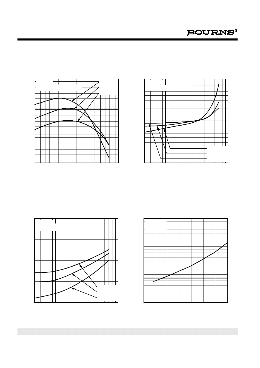
TYPICAL CHARACTERISTICS
Figure 4.
Figure 5.
Figure 6.
Figure 7.
TYPICAL DC CURRENT GAIN
vs
COLLECTOR CURRENT
I
C
- Collector Current - A
0·4
1·0
10
h
FE
-
T
y
p
ic
a
l
D
C
C
u
rre
n
t
Ga
in
10
100
1000
10000
TCD150AA
V
CE
= 5 V
t
p
= 300 µs, duty cycle <2%
T
C
= 125°C
T
C
= 25°C
T
C
= -30°C
COLLECTOR-EMITTER SATURATION VOLTAGE
vs
COLLECTOR CURRENT
I
C
- Collector Current - A
0·4
1·0
10
V
C
E
(sat
)
- Co
ll
e
c
to
r-Em
itte
r Sa
tu
ra
ti
o
n
Vo
lt
a
g
e
- V
0·1
1·0
10
TCD150AB
I
C
/ I
B
= 20
t
p
= 300 µs, duty cycle < 2%
T
C
= 125°C
T
C
= 25°C
T
C
= -30°C
BASE-EMITTER SATURATION VOLTAGE
vs
COLLECTOR CURRENT
I
C
- Collector Current - A
0·4
1·0
10
V
B
E
(sat
)
- Ba
s
e
-E
m
it
te
r Sa
tu
ra
ti
o
n
Vo
lt
a
g
e
- V
1·0
1·5
2·0
2·5
3·0
TCP150AC
T
C
= -30°C
T
C
= 25°C
T
C
= 125°C
I
C
/ I
B
= 20
t
p
= 300µs, duty cycle < 2%
COLLECTOR CUT-OFF CURRENT
vs
CASE TEMPERATURE
T
C
- Case Temperature - °C
-50
-25
0
25
50
75
100
125
I
CE
O
- Co
ll
e
c
to
r Cu
t-o
ff Cu
rr
e
n
t - µ
A
1·0
10
100
1000
TCD150AD
V
CE
= 400 V
I
B
= 0
TIP150, TIP151, TIP152
NPN SILICON POWER DARLINGTONS
5
JUNE 1973 - REVISED SEPTEMBER 2002
Specifications are subject to change without notice.
MAXIMUM SAFE OPERATING REGIONS
Figure 8.
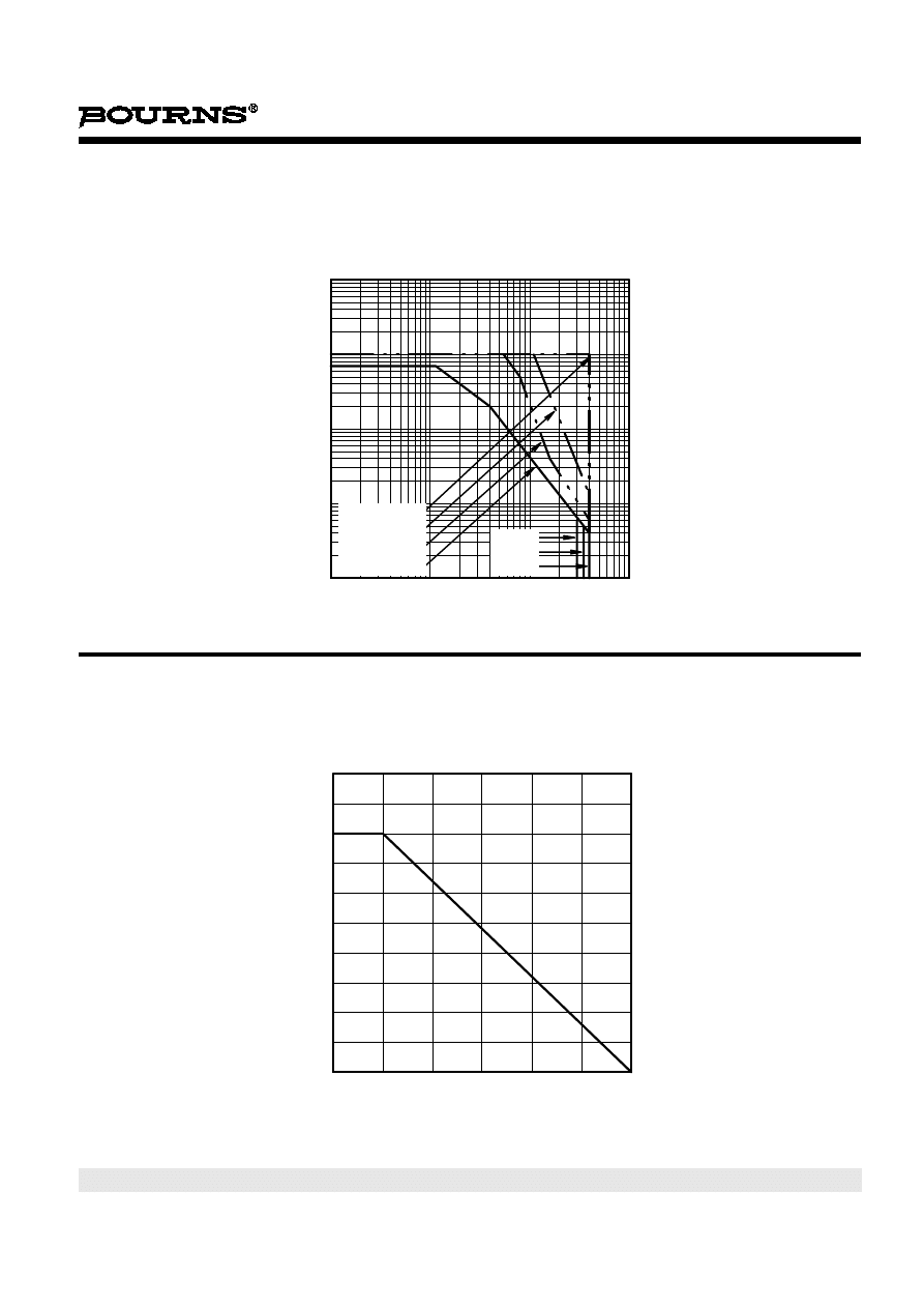
THERMAL INFORMATION
Figure 9.
MAXIMUM FORWARD-BIAS
SAFE OPERATING AREA
V
CE
- Collector-Emitter Voltage - V
1·0
10
100
1000
I
C
- Co
ll
e
c
to
r Cu
rre
n
t - A
0·01
0.1
1·0
10
100
SAD150AA
TIP150
TIP151
TIP152
t
p
= 0.1 ms
t
p
= 1 ms
t
p
= 5 ms
DC Operation
MAXIMUM POWER DISSIPATION
vs
CASE TEMPERATURE
T
C
- Case Temperature - °C
0
25
50
75
100
125
150
P
to
t
-
Ma
xi
mu
m
P
o
w
e
r D
issi
p
a
ti
o
n
-
W
0
20
40
60
80
100
TID150AA
Wyszukiwarka
Podobne podstrony:
TIP125, TIP126, TIP127 (Bourns)
TIP100, TIP101, TIP102 (Bourns)
TIP130, TIP131, TIP132 (Bourns)
TIP30 (Bourns)
TIP29 (Bourns)
więcej podobnych podstron