TIP125, TIP126, TIP127
PNP SILICON POWER DARLINGTONS
1
DECEMBER 1971 - REVISED SEPTEMBER 2002
Specifications are subject to change without notice.
●
Designed for Complementary Use with
TIP120, TIP121 and TIP122
●
65 W at 25°C Case Temperature
●
5 A Continuous Collector Current
●
Minimum h
FE
of 1000 at 3 V, 3 A
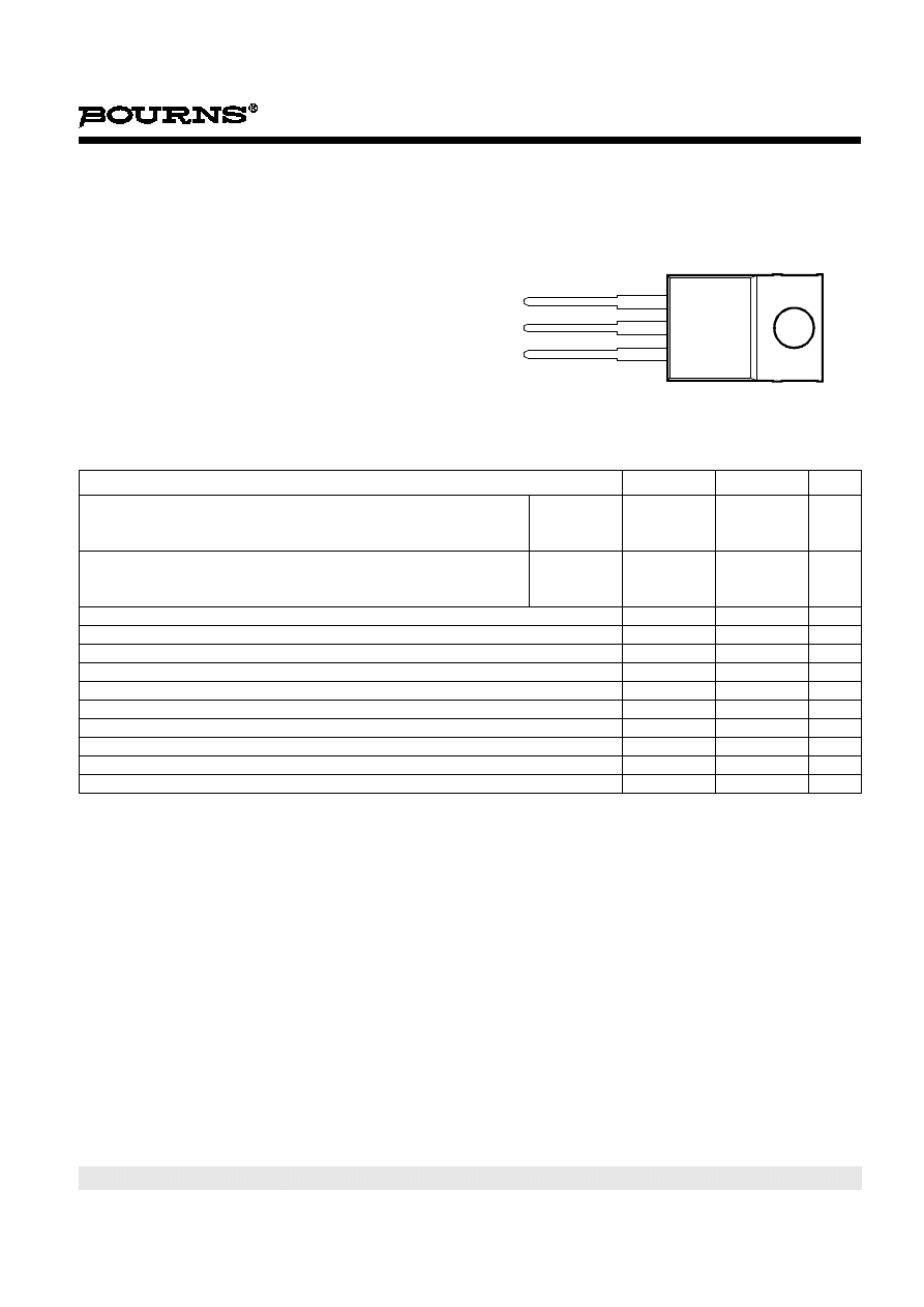
B
C
E
TO-220 PACKAGE
(TOP VIEW)
Pin 2 is in electrical contact with the mounting base.
MDTRACA
1
2
3
absolute maximum ratings at 25°C case temperature (unless otherwise noted)
NOTES: 1. This value applies for t
p
≤ 0.3 ms, duty cycle ≤ 10%.
2. Derate linearly to 150°C case temperature at the rate of 0.52 W/°C.
3. Derate linearly to 150°C free air temperature at the rate of 16 mW/°C.
4. This rating is based on the capability of the transistor to operate safely in a circuit of: L = 20 mH, I
B(on)
= -5 mA, R
BE
= 100
Ω,
V
BE(off)
= 0, R
S
= 0.1
Ω, V
CC
= -20 V.
RATING
SYMBOL
VALUE
UNIT
Collector-base voltage (I
E
= 0)
TIP125
TIP126
TIP127
V
CBO
-60
-80
-100
V
Collector-emitter voltage (I
B
= 0)
TIP125
TIP126
TIP127
V
CEO
-60
-80
-100
V
Emitter-base voltage
V
EBO
-5
V
Continuous collector current
I
C
-5
A
Peak collector current (see Note 1)
I
CM
-8
A
Continuous base current
I
B
-0.1
A
Continuous device dissipation at (or below) 25°C case temperature (see Note 2)
P
tot
65
W
Continuous device dissipation at (or below) 25°C free air temperature (see Note 3)
P
tot
2
W
Unclamped inductive load energy (see Note 4)
½LI
C
2
50
mJ
Operating junction temperature range
T
j
-65 to +150
°C
Storage temperature range
T
stg
-65 to +150
°C
Lead temperature 3.2 mm from case for 10 seconds
T
L
260
°C
TIP125, TIP126, TIP127
PNP SILICON POWER DARLINGTONS
2
DECEMBER 1971 - REVISED SEPTEMBER 2002
Specifications are subject to change without notice.
NOTES: 5. These parameters must be measured using pulse techniques, t
p
= 300 µs, duty cycle
≤ 2%.
6. These parameters must be measured using voltage-sensing contacts, separate from the current carrying contacts.
†
Voltage and current values shown are nominal; exact values vary slightly with transistor parameters.
electrical characteristics at 25°C case temperature
PARAMETER
TEST CONDITIONS
MIN
TYP
MAX
UNIT
V
(BR)CEO
Collector-emitter
breakdown voltage
I
C
= -30 mA
(see Note 5)
I
B
= 0
TIP125
TIP126
TIP127
-60
-80
-100
V
I
CEO
Collector-emitter
cut-off current
V
CE
= -30 V
V
CE
= -40 V
V
CE
= -50 V
I
B
= 0
I
B
= 0
I
B
= 0
TIP125
TIP126
TIP127
-0.5
-0.5
-0.5
mA
I
CBO
Collector cut-off
current
V
CB
= -60 V
V
CB
= -80 V
V
CB
= -100 V
I
E
= 0
I
E
= 0
I
E
= 0
TIP125
TIP126
TIP127
-0.2
-0.2
-0.2
mA
I
EBO
Emitter cut-off
current
V
EB
= -5 V
I
C
= 0
-2
mA
h
FE
Forward current
transfer ratio
V
CE
= -3 V
V
CE
= -3 V
I
C
= -0.5 A
I
C
= -3 A
(see Notes 5 and 6)
1000
1000
V
CE(sat)
Collector-emitter
saturation voltage
I
B
= -12 mA
I
B
= -20 mA
I
C
= -3 A
I
C
= -5 A
(see Notes 5 and 6)
-2
-4
V
V
BE
Base-emitter
voltage
V
CE
= -3 V
I
C
= -3 A
(see Notes 5 and 6)
-2.5
V
V
EC
Parallel diode
forward voltage
I
E
= -5 A
I
B
= 0
(see Notes 5 and 6)
-3.5
V
thermal characteristics
PARAMETER
MIN
TYP
MAX
UNIT
R
θJC
Junction to case thermal resistance
1.92
°C/W
R
θJA
Junction to free air thermal resistance
62.5
°C/W
resistive-load-switching characteristics at 25°C case temperature
PARAMETER
TEST CONDITIONS
†
MIN
TYP
MAX
UNIT
t
on
Turn-on time
I
C
= -3 A
V
BE(off)
= 5 V
I
B(on)
= -12 mA
R
L
= 10
Ω
I
B(off)
= 12 mA
t
p
= 20 µs, dc
≤ 2%
1.5
µs
t
off
Turn-off time
8.5
µs
TIP125, TIP126, TIP127
PNP SILICON POWER DARLINGTONS
3
DECEMBER 1971 - REVISED SEPTEMBER 2002
Specifications are subject to change without notice.
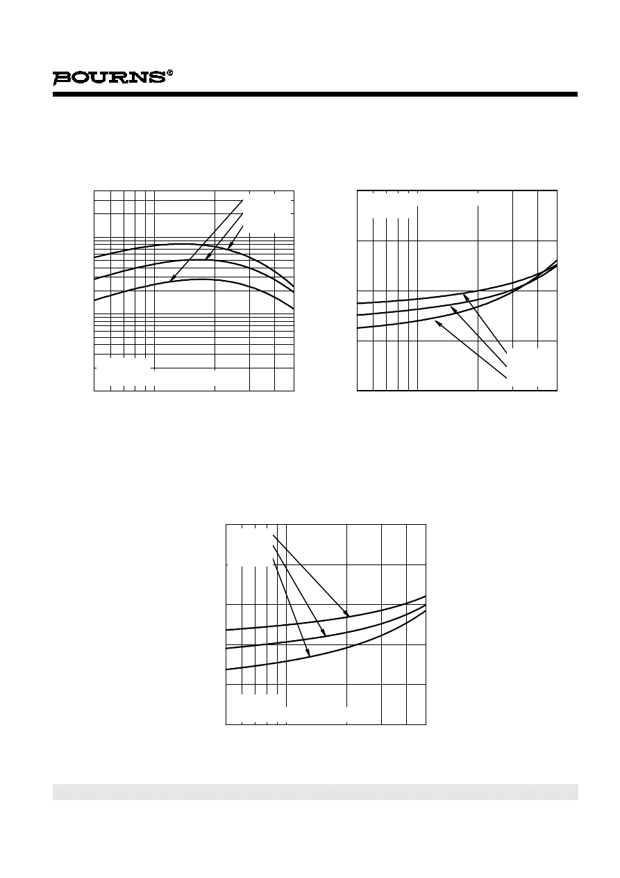
TYPICAL CHARACTERISTICS
Figure 1.
Figure 2.
Figure 3.
TYPICAL DC CURRENT GAIN
vs
COLLECTOR CURRENT
I
C
- Collector Current - A
-0·5
-5·0
-1·0
h
FE
-
T
y
pi
c
a
l
D
C
Cu
rr
e
n
t
G
a
in
40000
100
1000
10000
TCS125AA
T
C
= -40°C
T
C
= 25°C
T
C
= 100°C
V
CE
= -3 V
t
p
= 300 µs, duty cycle < 2%
COLLECTOR-EMITTER SATURATION VOLTAGE
vs
COLLECTOR CURRENT
I
C
- Collector Current - A
-0·5
-5·0
-1·0
V
CE
(s
a
t)
- Co
ll
e
c
to
r-E
m
itte
r
Sa
tu
ra
ti
o
n
Vo
lt
a
g
e
- V
-2·0
-1·5
-1·0
-0·5
0
TCS125AB
T
C
= -40°C
T
C
= 25°C
T
C
= 100°C
t
p
= 300 µs, duty cycle < 2%
I
B
= I
C
/ 100
BASE-EMITTER SATURATION VOLTAGE
vs
COLLECTOR CURRENT
I
C
- Collector Current - A
-0·5
-5·0
-1·0
V
BE
(s
a
t)
- Ba
s
e
-Em
itte
r Sa
tu
ra
ti
o
n
Vo
lt
a
g
e
- V
-3·0
-2·0
-2·5
-1·0
-1·5
-0·5
TCS125AC
T
C
= -40°C
T
C
= 25°C
T
C
= 100°C
I
B
= I
C
/ 100
t
p
= 300 µs, duty cycle < 2%
TIP125, TIP126, TIP127
PNP SILICON POWER DARLINGTONS
4
DECEMBER 1971 - REVISED SEPTEMBER 2002
Specifications are subject to change without notice.
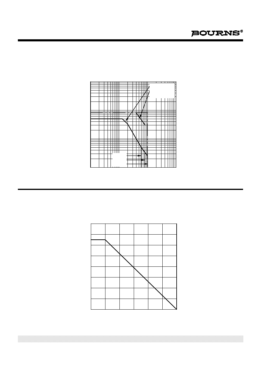
MAXIMUM SAFE OPERATING REGIONS
Figure 4.
THERMAL INFORMATION
Figure 5.
MAXIMUM FORWARD-BIAS
SAFE OPERATING AREA
V
CE
- Collector-Emitter Voltage - V
-1·0
-10
-100
-1000
I
C
- Co
ll
e
c
to
r Cu
rre
n
t - A
-0·1
-1·0
-10
-100
SAS125AA
DC Operation
t
p
= 300 µs,
d = 0.1 = 10%
TIP125
TIP126
TIP127
MAXIMUM POWER DISSIPATION
vs
CASE TEMPERATURE
T
C
- Case Temperature - °C
0
25
50
75
100
125
150
P
to
t
-
Ma
xi
mu
m
P
o
w
e
r D
is
s
ip
at
io
n
-
W
0
10
20
30
40
50
60
70
80
TIS120AA
Wyszukiwarka
Podobne podstrony:
TIP120, TIP121, TIP122, TIP125, TIP126, TIP127 (CDIL)
TIP125, TIP126, TIP127 (Fairchild Semiconductor)
TIP120, TIP121, TIP122, TIP125, TIP126, TIP127 (STMicroelectronics)
TIP150, TIP151, TIP152 (Bourns)
TIP125 127 (darlington)
TIP100, TIP101, TIP102 (Bourns)
TIP130, TIP131, TIP132 (Bourns)
TIP30 (Bourns)
TIP127
TIP29 (Bourns)
więcej podobnych podstron