Spectrum Analyzer Updates
Last update, Saturday, June 10, 2000
This part of the web page deals with the spectrum analyzer that Terry White (K7TAU)
and I described in QST for August and September of 1998, and the related Tracking
Generator appearing in November 1999.
The complete article is now available to be viewed and downloaded in
PDF format from ARRL. Go to the
and do a search on
spectrum analyzer. This will then get you to a point where the two part
paper can be downloaded.
Click this photo to see some tutorial info on the analyzer.
Crystal Filter for 30 kHz Resolution Bandwidth.
4May00
The latest refinement to the spectrum analyzer is a narrow filter using monolithic crystal
filter modules from ECS. These readily available parts offer an easy way to get a
resolution bandwidth of about 30 kHz, very useful for a variety of applications. (I
routinely use a 30 kHz RBW for IMD measurements here at W7ZOI.) This filter is the
collaborative effort of Fred Holler,W2EKB, and Jack Glandon, WB4RNO.
The first filter, built by Fred, uses a 4 pole filter set, sold as a set in two cans by Mouser.
The filter is designed to be terminated in 3Kat each end. This is realized with 0.5 inch
OD ferrite transformers using type 61material. This is a relatively low permeability
material (125)compared with some of the more popular mixes, which means that more
turns are required to achieve the needed inductance. (Jack also got good results with -43
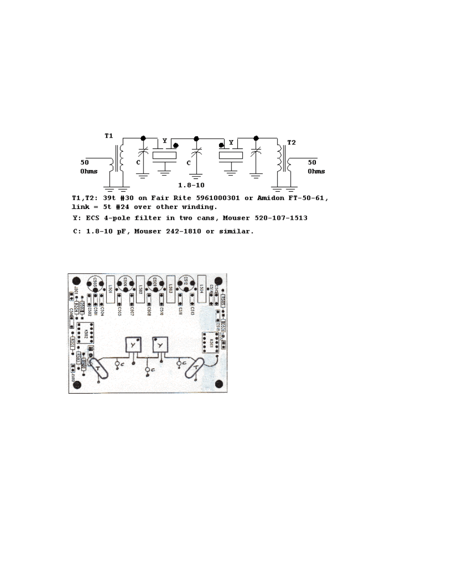
material, so use what you have.) The 4 pole filter is shown in the following schematic.
The filter elements are NOT symmetrical, so dots indicate the end next to the variable
coupling capacitor.
The next figure shows the layout used by Fred on the Kanga IF PC board.
The photo below shows two of the filters that Jack built. Shields were tried between
sections, but were not to be needed. The two filters were measured. Then, the two were
cascaded and measured again. The results are summarized in the table below.
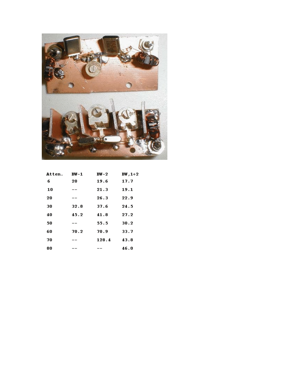
Bandwidth in kHz for various attenuation
values in dB.
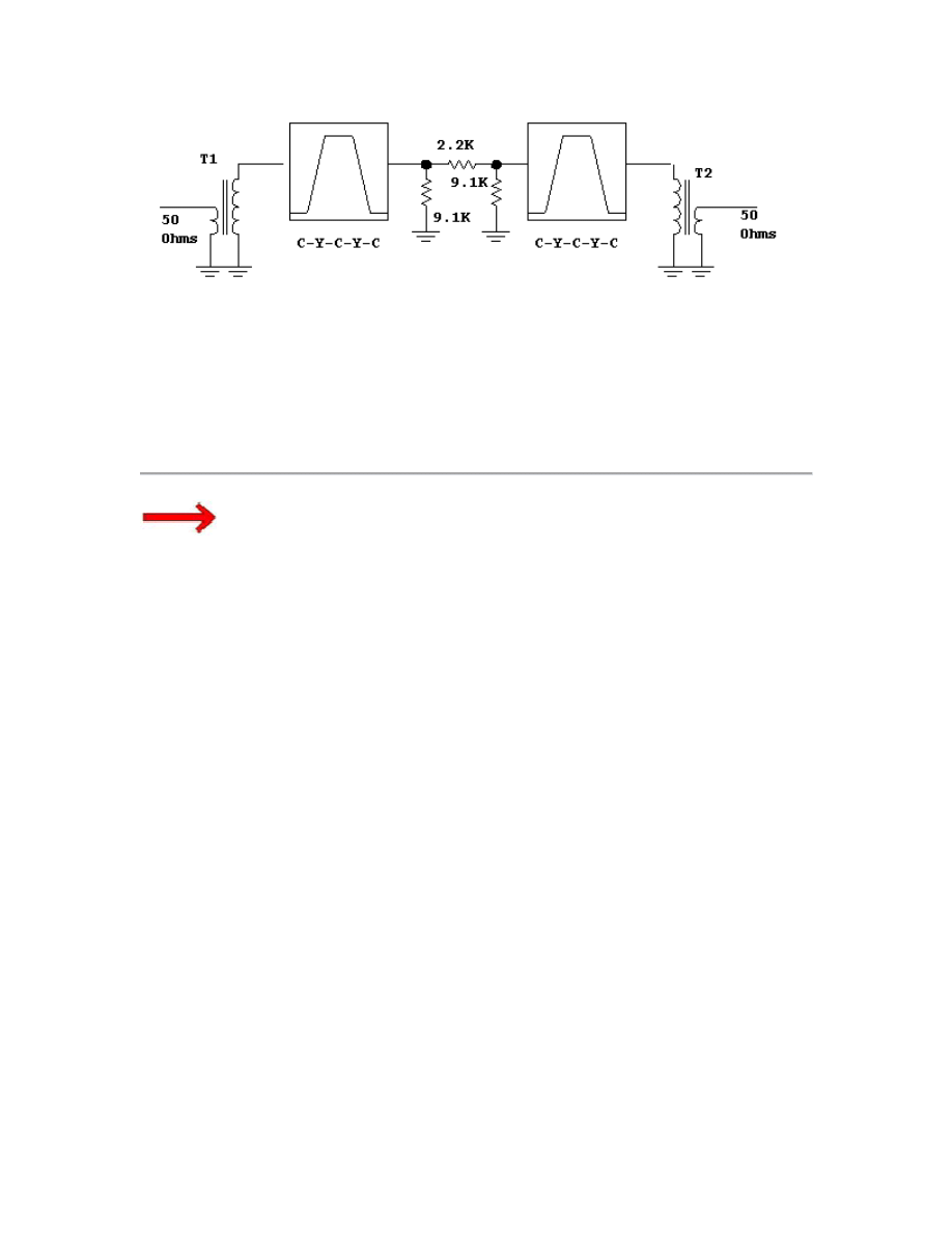
The schematic below is recommended by ECS when cascading two 4-polesets for an 8
pole response. The attenuator is a 6 dB pad with a Z0 of3K Ohms.
Jack has built this
topology and installed it in his analyzer. He reports a stopband attenuation over 90 dB.
Many thanks to both Fred and Jack fortheir efforts.
The results really look
outstanding, especially with 8 resonators. Narrow bandwidth is important in determining
resolution. Stopband attenuation should always be at least as much as the on -screen
display range. Indeed, even higher stopband attenuation is useful, for the analyzer can be
overdriven in some measurements.
(Jan10)
Coax Cable Applications in Building the SA and TG
As some of the builders start to get the tracking generator working, we are beginning to
see a few problems. Some are severe, but they are solvable.
It is important to recognize that the combination of a spectrum analyzer and a tracking
generator is a very difficult thing to build, mainly a result of the extreme shielding and
signal isolation required. The spectrum analyzer is a narrow bandwidth receiver capable
of displaying sub microvolt level signals. Yet the tracking generator is a transmitter that
is always generating a signal that is at exactly the same frequency as the sensitive
receiver. With an output of 0 dBm, the TG is at least 100dB higher than the sensitivity of
the analyzer, so this is the level of isolation required.
So, how do we get there? Good coax connectors should be used. The SA front-end, the
TG, and the SA 2nd LO and mixer should all be in well shielded boxes.The Hammond
boxes (1590B and 1590BB) have worked well for this application and are not terribly
expensive. All power and control lines in and out of the modules should route through
feedthrough capacitors.
In spite of these precautions, problems have been encountered. Here are some things that
can help:
First, the way the figures were presented in the QST articles lead to confusion. For
example, Fig. 8 of the August 1998 paper is partially duplicated as the "before" case
below. The "Preferred" case is the way we should have shown it.
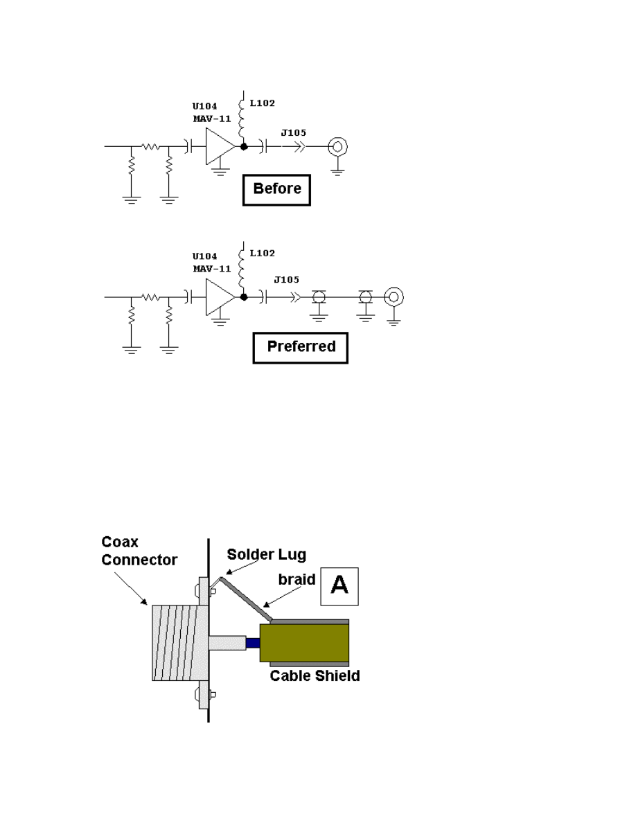
The difference between
the two circuits is in the use of coax cable. The
before
merely showed a wire from the
edge of the board to the coax connector center pin while the
preferred
form emphasizes
that
coaxial cable
should route the signal to the connector. The coax should be grounded
at both ends. This was
not
an ARRL drafting error, but a goof on our part in not being
more careful with our schematics.
Signals out of the tracking generator or into the SA front end should occur in a well
preserved coaxial environment. This has to do with the way we get from the internal
modules to the edge of the box housing the equipment.
This figure shows the way we
often use a coaxial connector. The connector resides in a hole in the panel. The coaxial
center wire from, for example the SA low pass filter, attaches to the center of the
connector while the braid is attached to the panel with a solder lug. This is a potential
problem, a shielding error. There is an open loop. Some signals that are flowing on the
inside
surface of the front panel will be near the connector. These will end upon the same
surfaces that carry the signals that are on their way to the SA low pass filter on the inside
of the coax. This constitutes mutual coupling between the two surfaces that will
intermingle them.
Here's one way to fix the problem:
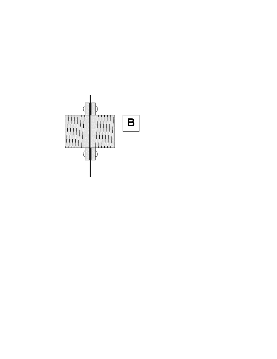
A bulkhead type coaxial connector is
now used to route signals from the "outside world," through the front panel to the coax on
the inside of the analyzer reaching the circuit modules. A male connector is needed on
each end of the inside cable, adding to expense. Moreover, the bulkhead connector is
expensive. But it is worthwhile. Prior to installing a bulkhead connector in my analyzer, I
could see a couple of spurious responses from local TV stations. When the bulkhead
connector (Fig. B above) replaced the BNC with solder lug (Fig. A above), the spurs
disappeared, even when the lid was off the box.
The same effect can be achieved with an extended shield:
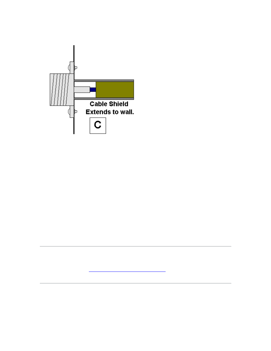
Here we extend the shield all the way to the front panel. The extension shown in the
figure is rather ideal, for it will come close to preserving the 50 Ohm environment. This s
not as vital at low frequencies as is the shielding integrity. It would be suitable, for
example, to push the braid up on the cable, solder the inner connector and insulate it, pull
the shield back down, and clamp a cylinder around coax to the wall. There should ideally
be no gaps in the shield surface such that there is no mutual surface shared by the inside
of the coax and the surfaces on the outside. Clearly there is room here for ingenuity.
These precautions are important for the analyzer input connections as well as the tracking
generator output. The integrity of the cable between the VCO and the tracking generator
is also important.
Many thanks to Jack, WB4RNO for his experimental results with the tracking generator.
Not all of the tracking generators built by hams are the simple ones like we have done
for low frequencies. For a homebrew TG that covers from DC to 1.8 GHz, take a look at
the work of KE5FX at
http://www.qsl.net/ke5fx/tr503.html
(Feb 9, 00).
Tracking Generator Errors
We have discovered a number of documentation problems with the Tracking Generator.
The board itself is fine, but some of the designators are wrong on the sheets going out
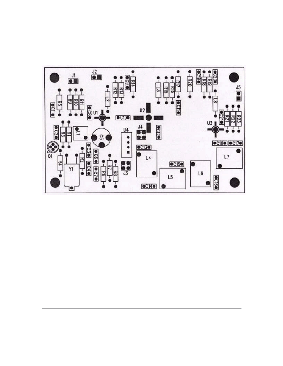
with the boards. Most of the errors occurred inthe crystal oscillator portion of the
schematic. The QST diagram (Fig.2) is OK and should be used for reference. C1 is 470
pF, although not very critical. C2 is .01 or 0.1 uf, again very non-critical. An updated
component map is shown in the figure below.
A capacitor, C20, was omitted from the QST schematic. This part is on the board and is a
470 pF disc. It's in parallel with C19. (In hindsight, this was a poor design choice! It's not
generally a good idea to parallel two bypass capacitors of differing value, for the
inductance of the larger capacitor can go parallel resonant with the smaller capacitor,
forming a high impedance at some frequency. A better wideband bypass would be twoor
more parallel caps, all with the same value. This was not a critical application and we
didn't get in trouble! Whew!)
The "roadmap" above and the schematic distributed with the Kanga boards have J
designator to go with the board input/output connections. They are properly shown above
and will be fixed in later Kanga schematics. The functions: J1=RF input from VCO,
J2=+15 volt supply, J3=Crystal oscillator power test point, J4=LO power test, and J5=RF
output. Note that U4 is the TUF-1H mixer.
Many thanks to Masa, JA3FR, and Sam, AE4GX for feedback on these errors.
Adding 2dB per division to the Spectrum Analyzer
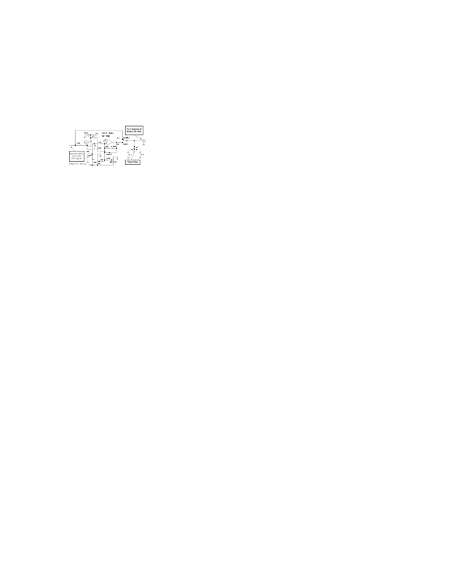
The majority of spectrum analyzer measurements are done with a vertical scale of 10 dB
per division. The log amp in the analyzer allows one to see about a 70 dB range of signals
at any one time with this setting. But, there are many situations when 1 or 2 dB per
division would be useful. These include filter adjustment and loss determination, filter
and resonator bandwidth measurements, and noise evaluation as part of a noise figure
measurement. A circuit to perform this is shown in the attached figure.
Click this photo for a larger view.
The circuit is nothing more than a DC amplifier with a voltage gain of 5. A signal change
that formerly occupied 1 vertical division now takes5,allowing one to see smaller
changes.
Circuit behavior is evident when you turn the analyzer on and calibrate it: Begin by
injecting a -30 dBm signal at the analyzer input with the scale factor set to 10 dB per
division. Calibrate the analyzer as before by adjusting IF gain to bring the response to the
top of the screen. Juggle the log gain and IF gain to achieve 10 dB per division, as
observed with the step attenuator. Now, with the signal still at the reference level (top of
the screen), switch to 2 dB per division. A signal may or may not be on screen, but
adjustment of R1 and/or R2 will produce it. You can now decrease the signal in 1 dB
steps with a step attenuator and watch the signal drop.
Set the scale back to 10 dB per division and reduce the generator signal to a value that
produces a signal just a few dB over the noise floor. Switching back to 2 dB/div and
adjustment of R1 and R2 will allow this signal to be observed.
This circuit has a side effect. The expanded resolution allows the deficiencies of the log
amp to be more easily observed. My present thinking is that it may be time to replace the
inexpensive and readily available MC3356 with the superior, but harder to obtain Analog
DevicesAD8307 log amp. Whenever one refines a measurement system, the deficiencies
become more observable.
The new circuit consists of two cascaded inverting amplifiers. The first has a gain of 2
while the second runs with a gain of 2.5, for a net gain of 5. The use of two inverting
stages allows an adjustable offset to be injected while maintaining constant gain. The new
circuit is added at the coax connector that feeds the Y-axis signal to the oscilloscope. Use
1or 2% tolerance resistors in this circuit, or at least in the gain determining parts.
The video filter circuit was modified to provide two video bandwidths. The newer one
(with the 3.3 uF) allows noise from a noise-diode to be averaged to produce a relatively
smooth line, useful in noise figure measurements. S2 is a center-off toggle switch
mounted on the front panel.

Construction is not critical. The signals are DC baseband values that have already been
detected and filtered, so they are not susceptible to the contamination that might plague
RF circuits. I built my amp on a small board scrap using "ugly" methods with the board
tucked into a corner of the instrument after operation was confirmed. There is no need to
shield this part of the circuit. About any dual op-amp will function well in this circuit. I
ran out of front panel room in my analyzer, so R1, R2 and S1are mounted on the side,
close to the front panel where adjustment is still easy. S1 is a miniature toggle type.
If desired, the circuit could be configured for 1 dB per division. This would require a DC
gain of 10, probably realized with gains of 3 and 3.33 in the two stages. The present
instrument produces a 4 volt Y-axis signal. A gain of 3 would crowd ranges, so it would
probably be convenient to re-calibrate the instrument for an oscilloscope sensitivity of 0.2
volt/division instead of the 0.5 presently used. This is easily done.
Give this refinement a try. It's simple, but adds a lot to the operational convenience. We
have no plans for boards for this--it's just too simple.
Attenuator Part Error
. The six input resistors in the 20 watt attenuator of Fig. 16 (Sept. 98
QST, p40) should be
620Ohms, 2 watt
, rather than 820 Ohms as shown.
Many thanks to
Jon, EA2SN.
Harmonic Distortion Measurements
One of the most common measurements we do with a spectrum analyzer is that of
harmonic distortion. This seemingly simple chore can be more difficult than we might
imagine, for harmonics can be created within the spectrum analyzer used for the
measurement.
Evaluation of a low power transmitter is an example of harmonic distortion measurement.
We assume that the transmitter output power has been measured. A power attenuator is
connected to the transmitter to drop the output tolevels that cannot damage the analyzer.
Some power attenuators built byW2EKB are shown below.
We must evaluate the spectrum analyzer to determine it's cleanliness before the
transmitter can be evaluated. This can be done with easily built outboard filters. The SA
that we described in QST was evaluated with the following experiments: First, an
HP8654A signal generator was set for a14 MHz output of -20 dBm and attached to the
analyzer. For harmonic distortion measurements, the analyzer is always operated with 10
dB attenuation, or more. We calibrated the analyzer to the -20 dBm signal and noted a
2ndharmo<
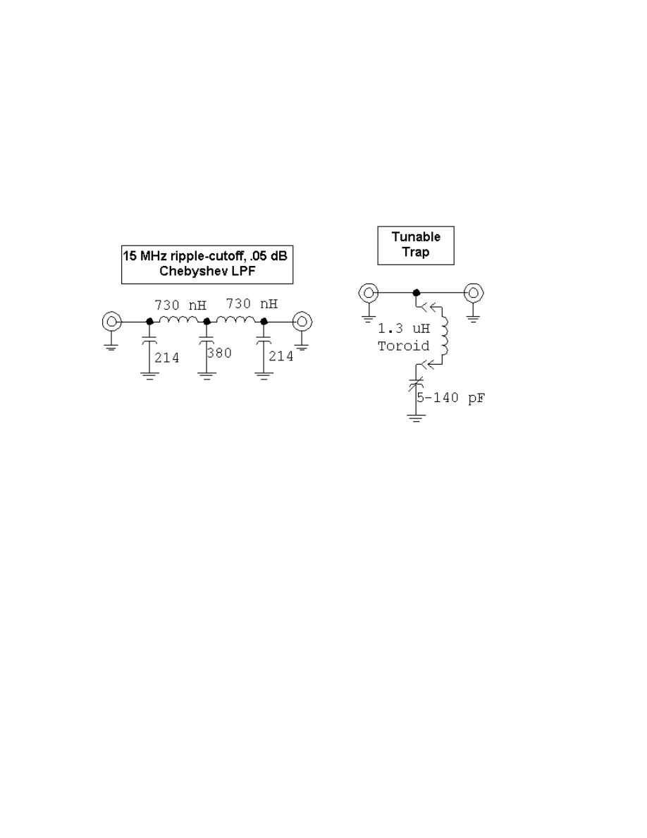
The low pass filter is removed and replaced with a tunable trap. This circuit was tuned to
attenuate the 14 MHz fundamental. This signal dropped by 37 dB, leaving the harmonic
unchanged. If the harmonic had been generated by the analyzer, there would have been a
substantial (well over 37 dB) drop in the harmonic's power level.
The trap was re-tuned to the 28 MHz 2nd harmonic. This dropped that level to -53 dBc,
leaving the fundamental power stable at -20 dBm. The displayed harmonic level would
not have changed if it had been generated in the analyzer front-end. The filter circuits are
shown below:
The low pass filter and trap were cascaded and placed between the generator and the
analyzer. This combination pushed the 2nd harmonic into the background noise, even
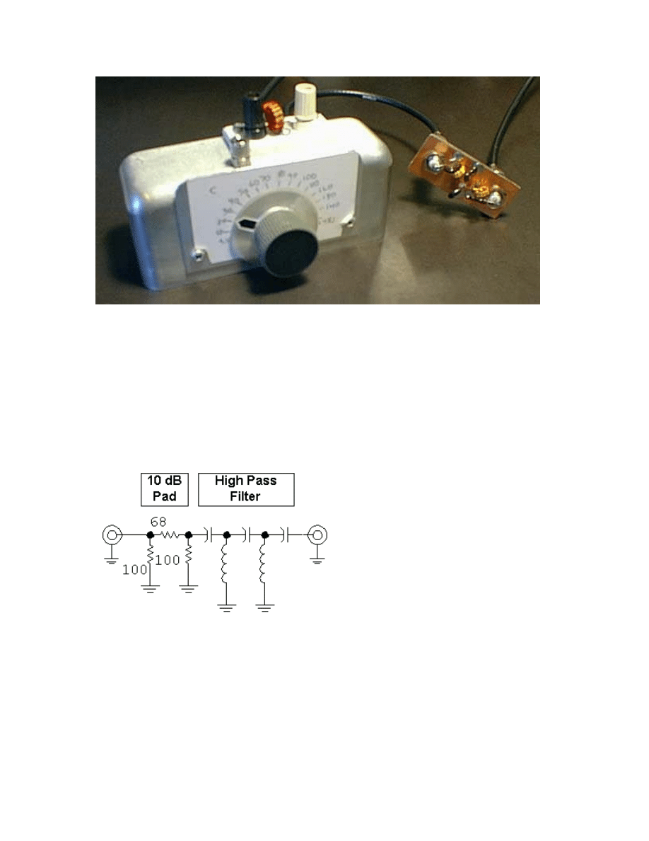
with the fundamental 10 dB above the top of the screen. The test set is shown in the
photo below:
These measurements have confirmed the cleanliness of the analyzer for harmonic
measurements. We can now attach the attenuated transmitter output to the analyzer and
meaningfully determine harmonic distortion.
But, what would we do if the analyzer was generating some harmonics in its own front-
end? This is a common situation with many commercial analyzers. All is not lost.
Harmonics can be evaluated by a two step measurement. The fundamental power is first
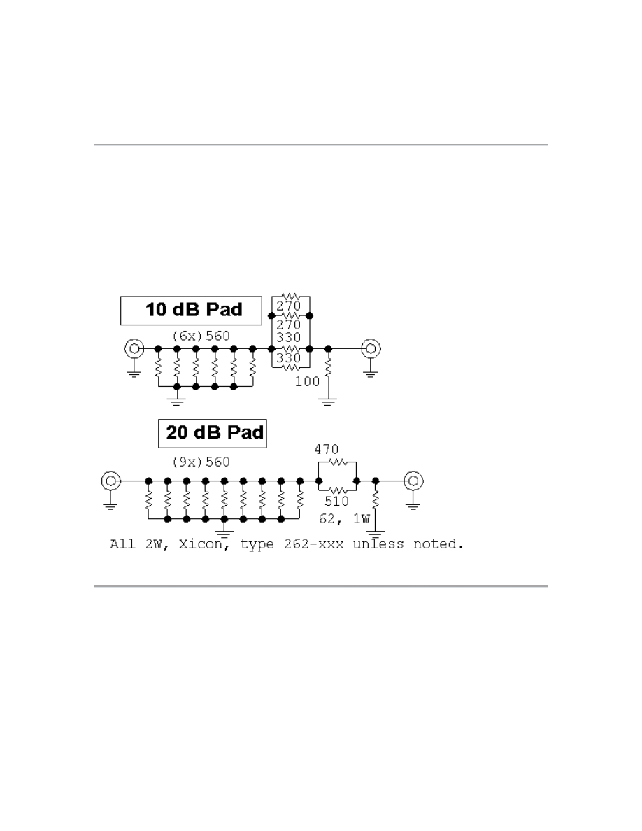
determined by examining the output of the source being studied. The following circuit is
then inserted in the source output line.
The input of this module is a pad with approximately 10 dB attenuation. Analyzer gain
must be increased by this amount to compensate for the loss. The extra pad guarantees
that the source sees a wideband 50 Ohm load. The pad is followed by a 5th order high
pass filter that drives the analyzer. This serves to attenuate the fundamental by 25 to 30
dB if the filter was designed for a ripple cutoff just below the 28 MHz 2nd harmonic
frequency. This will probably push the self-generation of harmonics within the analyzer
to the point that they are no longer significant.
The tuned trap shown earlier can also be used in this application. It's still useful to insert
the extra pad. The function we seek is to reduce the "loud" signal reaching the analyzer
that causes the internal distortion.
Power attenuators
are needed ahead of the analyzer when testing transmitters. We
presented one in the article, but then discovered that the 2 watt AB resistors we used are
no longer available, a familiar story these days. But Fred, W2EKB, came to the rescue.
He purchased some Xicon resistors from the current Mouser catalog and built a couple of
pads, shown below. He used some copper straps to improve the grounding. The circuits
were built in the Hammond 1590B boxes. Testing showed that they were clean through
150 MHz.
Many thanks Fred !
Using RCA connectors
Here's a great tip for folks fighting the problem of expensive coaxial cable and the even
more expensive connectors; a scheme for using
RCA connectors
. Here's what Barry
Lennox sent to us on this subject:
1. Take a 4" pigtail of good high coverage braid (I use silver-plated stuff from RG-
400) and sweat it all around the outer metal rim of the phono plug.I have made a
little jig from wood and a bit of wire and tube, to support things, and make several

in one sitting as they only take a few minutes, and are very useful to have in-
stock.
2. When you need to terminate a cable, bare about 0.5" of the inner, and about4" of
the outer jacket leaving the braid exposed.
3. Push the cable inside the pigtail braid (pre-expand it a bit) then use a 4" length of
heat-shrink to clamp the two braids together.
4. Finally solder the inner wire to the pin, as normal; and you have a fast and neat
connection.
The reason for preparing the connectors and braid ahead of time is to prevent melting
insulation.
Many thanks, Barry!
Update: I recently needed a cable for an RCA connector and tried this scheme. It works
great, although it took some practice on the first connector. (Oct 99)
MAV-11 pinout
: Some of the data sheets that went out with the Kanga boards were in
error with regard to pinout for these parts. The dot is on pin three, which is the output pin
in the MAV-11. The information in the paper was correct.13 Feb 99.
A Block Converter
Our lab includes a tunable block converter. This consists of nothing more than a POS200
VCO (approximately 100 to 200 MHz), a three dB pad, and a SBL-1 mixer. The mixer
was available in the junk box and can be driven directly from the POS mixers. A front
panel pot tunes the VCO, allowing the VHF range to be hetrodyned down to the analyzer
baseband. The pad is in the signal path, bringing the overall conversion loss to an even
10dB. Other mixers and VCOs will allow other parts of the spectrum to be examined. No
schematic is presented.
The converters are used with an external step attenuator. 13Feb99.
A Zero-Span Mode.
A common feature in commercial spectrum analyzers is a "zero span" mode. This mode
merely eliminates the sweeping of the VCO, turning the analyzer into a receiver that is
tuned with the center frequency control. This is especially useful if you wish to measure
the local oscillator with a frequency counter to establish center frequency. The zero-span
mode is realized in our box by placing a switch in the path from the sweep generator to
the VCO. This is easily performed with a JFET switch as shown in the figure
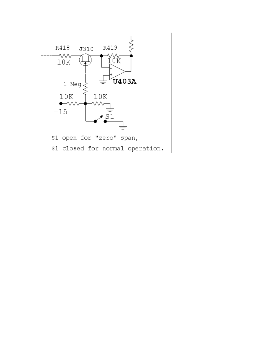
This modification has been added to an analyzer built by Jim Cotton,N8QOH, at Western
Michigan University. Jim used an ECG457 FET as a replacement for the J310 suggested.
As Jim points out, about any N channel JFET should work fine. A small error occurs
when the sweep is stopped that causes about a 20 or 30 kHz shift in VCO frequency, but
this is not a problem with wide resolution bandwidths. The tracking generator sample
output from the VCO is counted when the zero-span mode is active. Many thanks for the
feedback Jim!
If you want to see Jim's analyzer in detail,
has a wonderful collection of
photos, including inside shots of most modules. Nice job Jim!
Fred, W2EKB, suggested an even easier mod to achieve the "zero span" modification.
This is shown below:
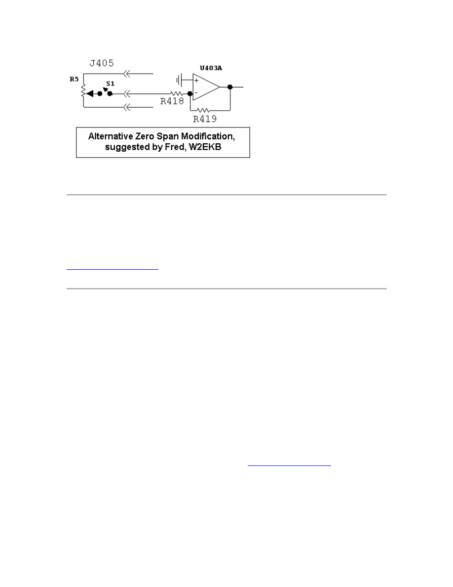
This variant has the advantage that
no change is required on the time base board. Many thanks Fred!
Component Collections:
Circuit boards and Parts "Kits" are available through Kanga USA for both the spectrum
analyzer and the tracking generator. These are not kits in the traditional "Heath" sense,
for they have no step by step instruction manuals. For more information go to
Parts Problems--Sources for Purchasing.
Some folks have encountered parts procurement problems. I have had good luck with
special items by ordering from Future Active Electronics, Inc. They have local offices all
over the country, but they are a mail order house. I was able, through Future, to buy
Motorola MC3356P chips, Analog Device IF chips, J310 JFETs, to name just a few
items. I've had friends within the industry also offer positive comments about these folks.
Try1-800-655-0006. A US address to obtain a catalog or place an order is Department
SF1, 41 Main Street, Bolton, MA 01740. Future Active is an international company with
outlets in several countries. Some outlets WILL NOT sell in small quantities.
Quartz Crystals are always a problem these days. The classic source that we could all
depend upon in the past seems to have dried-up for the amateur market--they now have a
minimum order that is just large enough that it is not possible to purchase just one crystal
at a time! But, as is usually the case, anew supplier shows up to take over. My new
choice is Hy-Q International. Their web address is
After getting
to the home page, go to the appropriate country. The phone number in the US is 606-283-
5000.Standard delivery time is 3 weeks (which they met with my order), the price sare
very competitive, and they didn't flinch at my wanting to order a single crystal.
The LO crystal to order is a 5th overtone, HC-49, 20 pF (not critical) 0-50 ° C , 10 ppm
Temperature drift, 5 ppm Calibration accuracy. This is what I ordered, but few
parameters are critical in this application. One could even get by with a free running LC
oscillator in this application.
Two crystals I ordered arrived and were tested (Sept. 15
th
). They both came up without
problem with the same output power that was extracted from an earlier crystal. The
frequency I measured was just over 1 kHz below 100 MHz, which is well within the
specifications that I used when ordering. It's a thumbs up vote on Hy-Q from W7ZOI
.
T301
is
10 bifilar turns on an Amidon FT37-43 or similar ferrite core. Wire size
really doesn't matter and #28 is fine. This is not a critical part use whatever ferrite you
have in the junk box. (Thanks to KG0SB, KA7EXM,and others who caught this.)
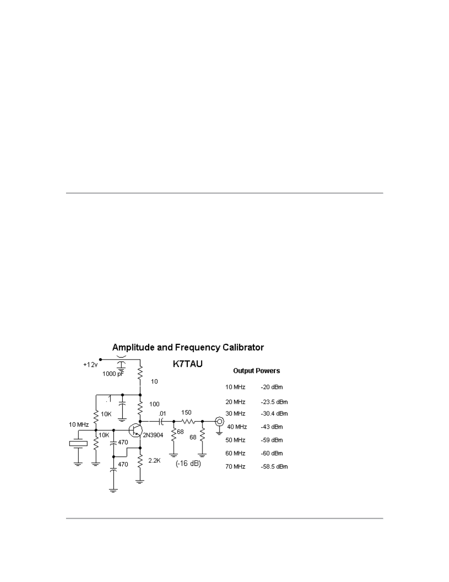
A Crystal Calibrator
The analyzer that was photographed for the QST article was the one that Terry built. He's
the resident
master
craftsperson around this part of the world. His analyzer included the
calibrator shown below.
This circuit is a crystal controlled Colpitts oscillator with output extracted from the
collector, a point in the circuit that is rich in harmonics. The pad (16 dB in Terry's
analyzer) is adjusted to provide an output of-20 dBm at the 10 MHz fundamental. If you
want to add a pot to adjust the amplitude, replace the 150 Ohm resistor in the pad with a
100 Ohm pot and100 Ohm series fixed R. The calibrator is calibrated against a high
quality signal generator, if available.

Assorted Comments and Errors
In
Figure 9
,J12 should be shown connecting to J3, Figure 8; J13 connects to J4 in
Figure 7. tnx to Bill Dawson, K6VPE via W1VD via N1FB at ARRL.
MiniCircuits MAV-11 ICs are used in three places in the analyzer. They are biased with a
pair of paralleled 220 Ohm resistors. The power dissipation in a single 110 Ohm R would
exceed 1/4 watt. Note that the dot on the MAV-11 goes with pin 3, the output.
The question of a narrow
,
homebrew crystal filter
has come up in
discussions. We will do some experiments and report the results here. Right now, it looks
like 3 kHz is about as narrow as you should go. Even then, the filter should be one with 2
to4 crystals, ideally with a rounded peak shape. You don't want the same flat topped filter
here that you might use for communications. If even narrower bandwidths were used, the
first LO would need to be phase locked to a stable reference. The crystal filters we used
were from a local surplus source and are not generally available. The analyzer is
practical, even without the crystal filter, so you can add it later.
A commercial crystal filter could be used. The builder would then have to add matching
networks at the filter input and output to transform from 50 Ohms to the impedance that
the filter "wants." The networks, even if they use toroids, may need some shielding to
keep one network from coupling to the other.
The
10 MHz filter board
includes a 4
th
order LC bandpass filter for the wider
resolution bandwidth. The board layout was done for 8 mm variable capacitors, but the
QST schematics called for the 10 mm plastic variables. The larger parts still fit on the
board.
The 10 MHz L/C filter is easily moved to 10.7 MHz, if you happen to have crystal filters
at that frequency. To move the LC filter, changeC504 and C513 from 120 to 110 pF, and
shift C507 and C510 from 180 to 160pF. Many thanks to Steve, AA7U.
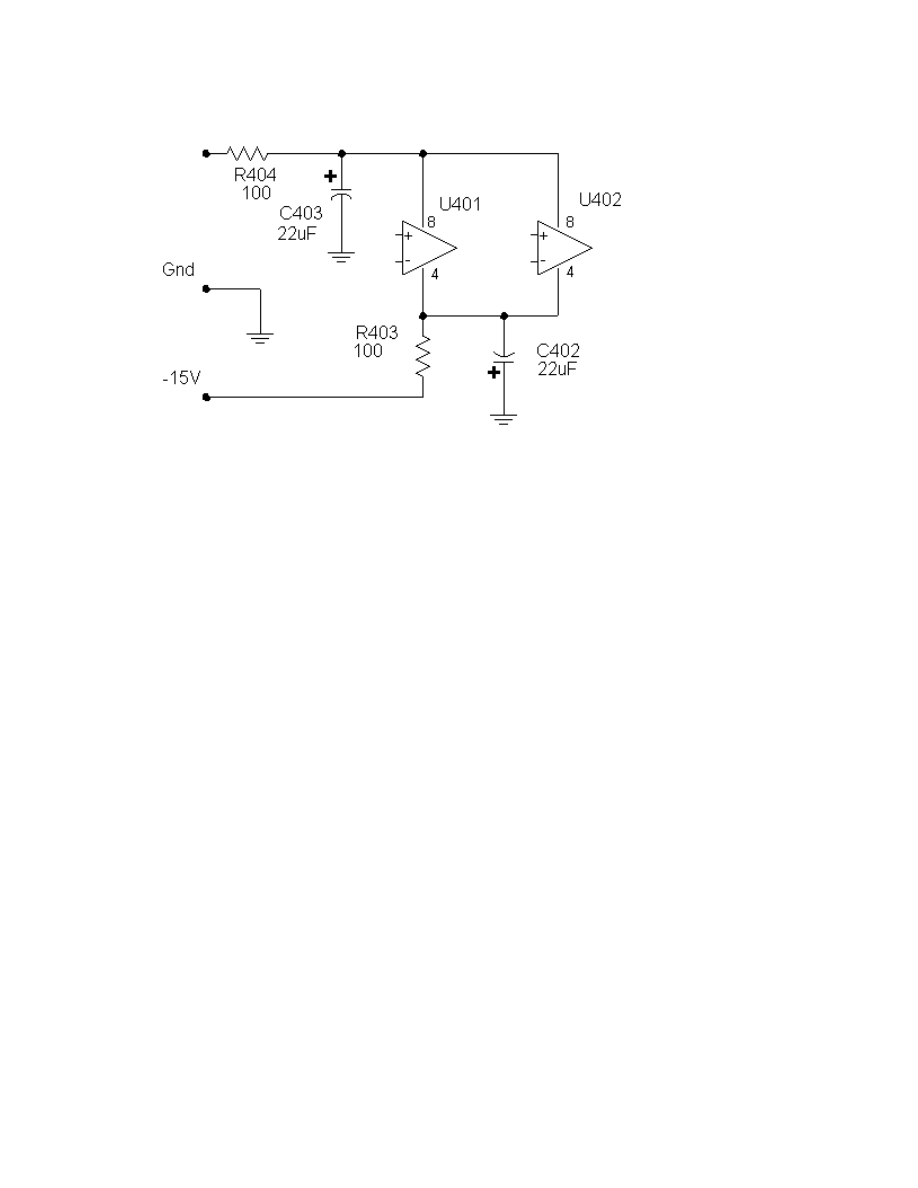
Figure 2, the Time Base
, had a colossal mistake in it. In the upper left corner of the
figure we find that the +15 volt power supply is grounded. We really didn't want to do
this, and the boards do not include this "feature." The correct schematic is shown below
ina figure that presents just the power supply connections for U401 and U402.The 3
rd
op-
amp, U403, has its own similar de-coupling network. Many thanks to reader Nicholas
Caruso!
Many thanks
to all the builders who have offered feedback.
Wyszukiwarka
Podobne podstrony:
EMC Spectrum Analyzer v2
EMC Spectrum Analyzer v2
How the ABI Prism 310 Genetic Analyzer Works
updatejpegprocessing(1)
cpu364 update instructions
In vivo MR spectroscopy in diagnosis and research of
Bluetooth update AVIC Fxxx Ver330
2wyklad 06 analyzer id 32779 Nieznany (2)
Instrukcja Aktualizacji modelu KDL 32EX720 TV Firmware update
cpu363 update instructions
5 4 5 Lab Create Accounts and Update
spectral tworzywa sztuczne, Elektra boczki
Quick Look at Gun Control Analyzing the Issue From Both Si
mpdm upDATE
SOP, Sop-wyklady Brzezinski update!, Programowanie współbieżne
Instalacja ROMów KDZ Updater LG L9 P760
Optical Spectroscopy Of Nanophase
więcej podobnych podstron