
JOURNAL OF MICROELECTROMECHANICAL SYSTEMS, VOL. 7, NO. 1, MARCH 1998
69
Low-Stiffness Silicon Cantilevers with Integrated
Heaters and Piezoresistive Sensors for High-Density
AFM Thermomechanical Data Storage
Benjamin W. Chui,
Student Member, IEEE,
Timothy D. Stowe, Yongho Sungtaek Ju,
Kenneth E. Goodson, Thomas W. Kenny, H. Jonathon Mamin, Bruce D. Terris,
Robert P. Ried,
Member, IEEE,
and Daniel Rugar,
Member, IEEE
Abstract— Single-crystal silicon cantilevers 1
m thick have
been demonstrated for use in high-density atomic-force micro-
scopy (AFM) thermomechanical data storage. Cantilevers with
integrated piezoresistive sensors were fabricated with measured
sensitivities
1R=R up to 7.5 2 10
07
per ˚
A in close agreement
with theoretical predictions. Separate cantilevers with integrated
resistive heaters were fabricated using the same basic process.
Electrical and thermal measurements on these heating devices
produced results consistent with ANSYS simulations. Geometric
variants of the cantilever were also tested in order to study the
dependence of the thermal time constant on device parameters.
Depending on the design, time constants as low as 1
s were
achieved. A thermodynamic model was developed based on the
cantilevers geometry and material properties, and the model was
shown to predict device behavior accurately. A comprehensive
understanding of cantilever functionality enabled us to optimize
the cantilever for high-speed thermomechanical recording. [264]
I. I
NTRODUCTION
M
ICROMACHINED cantilevers have been widely used
in atomic-force microscopy (AFM) for imaging pur-
poses [1]–[3]. Alternate uses have also been explored, for
example in nanolithography [4]–[6] and high-density data
storage [7]–[10]. This paper describes recent developments
in one AFM-based recording technique in particular, that
of thermomechanical data storage [11], with a focus on the
integration of heating and deflection-sensing elements onto the
micromachined cantilevers.
In AFM thermomechanical data storage, digital information
is represented as submicron data pits on a rotating substrate.
In a typical implementation, the sharp tip of a cantilever
is kept in continuous contact with a spinning polycarbonate
disk by a weak loading force on the order of 10
N. For
writing, the cantilever tip is heated above the glass transition
Manuscript received April 17, 1997; revised October 25, 1997. Subject Edi-
tor, K. Petersen. This work was supported by an IBM Cooperative Fellowship,
the National Science Foundation CAREER Program (ECS-9 502 046), the
National Science Foundation Instrumentation for Materials Research Program
(DMR-9 504 099), and the Charles Lee Powell Foundation. The work of H.
J. Mamin and R. P. Ried was supported in part by ARPA Contract DABT63-
95-C-0019.
B. W. Chui, T. D. Stowe, Y. S. Ju, K. E. Goodson, and T. W. Kenny are
with the Departments of Electrical Engineering and Mechanical Engineering,
Stanford University, Stanford, CA 94305-4021 USA.
H. J. Mamin, B. D. Terris, R. P. Ried, and D. Rugar are with IBM Research
Division, Almaden Research Center, San Jose, CA 95120-6099 USA.
Publisher Item Identifier S 1057-7157(98)02038-1.
(a)
(b)
Fig. 1.
Principle of thermomechanical data storage using (a) cantilevers
with built-in heaters for writing and (b) integrated piezoresistive sensors for
readback.
temperature of polycarbonate (which is approximately 120 C
while subjected to the loading force, thereby melting data pits
onto the substrate. For reading, the cantilever deflection is
measured as the tip rides over the pits. Bit densities up to
30 Gb/in (50 times CD-ROM) have been demonstrated [12].
With low-mass cantilevers, readback rates up to 1.2 Mb/s have
been achieved [12].
Originally, writing was achieved by heating the tip with
a laser beam, and reading was achieved by measuring the
deflection of a second laser beam off the cantilever. A major
disadvantage of this method is that the lasers are bulky and
require precise alignment. While some simplification has been
obtained using a tapered optical fiber as a cantilever [13], the
ultimate goal is to develop cantilevers with integrated reading
or writing elements that do not rely on lasers, as shown in
Fig. 1. For this purpose, we have developed single-crystal
silicon cantilevers with piezoresistive elements for readback,
based on the approach of Tortonese et al. [14]–[16]. We have
also made separate cantilevers with integrated resistive heaters
for writing [17], [18].
The ideal integrated cantilever will have to satisfy many
conditions simultaneously. In order to read marks at densities
of 20–50 Gb/in , it must have a tip with a radius of curvature
below 500 ˚
A To achieve adequate signal-to-noise ratio, it
needs a sensor capable of detecting 10 ˚
A of motion in the
readback bandwidth. The device must be soft, with a stiffness
of 1 N/m or less, to allow for operation at loads below 10
N, which is necessary to avoid wear of the tip or sample. At
the same time, the resonant frequency should be as high as
possible. The combination of low stiffness and high frequency
requires the cantilever to have low mass. For writing, an
1057–7157/98$10.00
1998 IEEE
Authorized licensed use limited to: Politechnika Slaska. Downloaded on May 29, 2009 at 04:22 from IEEE Xplore. Restrictions apply.
70
JOURNAL OF MICROELECTROMECHANICAL SYSTEMS, VOL. 7, NO. 1, MARCH 1998
Fig. 2.
Fabrication process for 1-
m-thick cantilevers.
integrated element for heating the tip is required, and the
thermal time constant should be as short as possible, preferably
on the order of 1
s.
In this work, we have focused on two areas in partic-
ular. First, we have integrated piezoresistive sensors with
cantilevers that are at least two times thinner than previous
devices [14]–[16]. With a cantilever of stiffness 1 N/m, we
have measured a deflection sensitivity of 0.016 ˚
A
Hz and
a calculated resonant frequency of 280 kHz. To achieve
this combination, we had to use novel processing techniques
involving rapid thermal anneal to make thin cantilevers 1
m thick with piezoresistors confined to less than half the
cantilever thickness. Second, we have fabricated cantilevers
with integrated electrical heating elements and have observed
thermal time constants as low as 1
s We have implemented
both types of cantilevers on a rotating sample to demonstrate
reading and writing without lasers.
II. C
ANTILEVER
F
ABRICATION
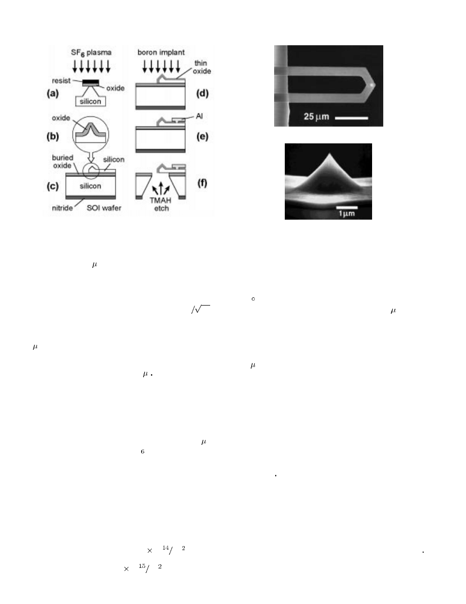
The fabrication process for the cantilevers, shown in Fig. 2,
has been adapted from reference [16]. The starting material
is a silicon-on-insulator (SOI) wafer [19] with a 5- m-top
silicon layer. In Fig. 2(a), an SF
plasma etch is used to
undercut an oxide-resist mask to form a blunt tip, which is
then sharpened by low-temperature oxidation [Fig. 2(b)]. In
Fig. 2(c), the cantilever itself is patterned and 1000 ˚
A of
thermal oxide is grown to form an electrical passivation layer.
(Because the oxide layer is thin, the curvature of the finished
cantilever due to stress in the oxide layer is insignificant.)
After this step, in a departure from [16], which calls for
preoxidation implantation, a series of boron implants are
performed through the 1000 ˚
A of oxide [Fig. 2(d)]. In the
case of the piezoresistive cantilevers, a first boron implant is
performed at 40 keV with a dose 5
10
cm to form the
piezoresistive layer, and a second boron implant is performed
at 40 keV with a dose of 5
10
cm to produce heavily
(a)
(b)
Fig. 3.
Scanning electron microscope images of (a) released cantilever and
(b) tip.
doped ohmic contact regions. (The implant sequence used to
make the heaters is slightly different and will be described
in the next section.) Instead of a conventional furnace anneal,
the implants are activated by a 10-s rapid thermal anneal at
1000
C in order to minimize boron diffusion. This results
in a shallow piezoresistive layer extending 0.4
m below
the cantilever surface [20]. In general, the shallower the
piezoresistive layer relative to the overall cantilever thickness,
the better the performance of the resulting piezoresistive
sensor. A variant of this rapid thermal anneal method has been
adopted by Ried et al. in producing piezoresistive cantilevers
0.34
m thick [21]. In Fig. 2(e), contact vias are etched
through the oxide, and aluminum is deposited and patterned
to form electrical connections to the cantilever. A backside
etch in tetramethyl ammonium hydroxide solution is used to
remove the bulk silicon underneath the cantilever [Fig. 2(f)].
A low-stress polyimide layer and a one-sided etch setup is
used to protect the front side of the wafer during this step.
Finally, the polyimide is removed in an oxygen plasma etch
to release the cantilevers.
Fig. 3 shows an scanning electron microscope (SEM) mi-
crograph of a fabricated cantilever and a close-up of the tip.
The tip is seen to be very sharp, with a radius of curvature
below 300 ˚
A Such a tip should be suitable for reading and
writing marks on a 1000- ˚
A scale.
III. C
HARACTERIZATION OF
P
IEZORESISTIVE
C
ANTILEVERS
The sensitivity of the piezoresistive cantilevers was mea-
sured by placing the cantilever on a piezoelectric actuator
(which is part of an AFM) and oscillating the cantilever
support with the tip in contact with a fixed surface. Typ-
ical oscillation amplitudes were on the order of 1000 ˚
A
The piezoresistive response for a given oscillation amplitude
was measured with a simple full bridge circuit based on a
Authorized licensed use limited to: Politechnika Slaska. Downloaded on May 29, 2009 at 04:22 from IEEE Xplore. Restrictions apply.

CHUI et al.: CANTILEVERS WITH HEATERS AND SENSORS FOR DATA STORAGE
71
TABLE I
C
OMPARISON OF
P
IEZORESISTIVE
C
ANTILEVERS FROM
T
HIS
W
ORK AND
T
ORTONESE
et al.
Fig. 4.
Noise spectrum of a 75-
m piezoresistive cantilever. The theoretical
Johnson noise floor is shown as the dotted line. Inset: cantilever response to
100- ˚
A modulation.
Burr–Brown INA103 instrumentation amplifier. This amplifier
has an input noise of 1 nV
Hz and a gain-bandwidth product
of 100 MHz. We operated with a bridge supply voltage of
5 V (i.e., 2.5 V across each resistor) and a gain of 100.
Since the cantilever resistance was 5–30 k
(depending on
length and doping concentration), the power dissipated in the
cantilever was 1 mW or less. Measured values of piezoresistive
sensitivity obtained for cantilevers of various lengths were in
close agreement with theory [16], [17].
For a 75- m-long cantilever, a piezoresistive sensitivity
of 7.5
10
per ˚
A was measured. This compares
favorably to other piezoresistive sensors, while our device has
much lower stiffness. Compared with Tortonese et al. [15],
[16], our cantilever has a more favorable force figure of merit
due to its lower spring constant (Table I).
Fig. 4 shows the noise spectrum of a 75- m-long cantilever.
The observed noise floor of 1.6 10
˚
A
Hz is very close to
the Johnson noise floor of 1.3
10
˚
A
Hz With its knee
around 200 Hz, the integrated
noise from 1–200 Hz is
only about 0.5 ˚
A The inset of Fig. 4 shows the response of the
cantilever to a 100- ˚
A oscillation applied with the AFM. The
measurement bandwidth used in this experiment was 1–100
kHz, within which the minimum detectable displacement was
below 10 ˚
A Since data pits on the polycarbonate disk are
typically 100–200 ˚
A deep, piezoresistive readback of real data
pits should be possible at this bandwidth.
Fig. 5 shows readback signals obtained simultaneously for
a pair of 150- m-long piezoresistive cantilevers operated in
parallel. The cantilevers were operated on a spinning silicon
test sample with a rectilinear pattern of 1100- ˚
A-deep grooves.
The bandwidth in this case was 30 kHz, and the linear velocity
Fig. 5.
Readback signals obtained in parallel with two 150-
m piezoresistive
cantilevers operated on a spinning test sample with 1100- ˚
A-deep grooves.
was approximately 20 mm/s. No independent load control was
used for the cantilevers. Because of the low stiffness of the
cantilevers, however, it was possible to bring both tips into
contact with the sample while maintaining acceptably low
loading forces, in this case below 5
10
N. Because these
cantilevers were relatively long, the sensitivity and bandwidth
were not as high as with the 75- m cantilever described in
Fig. 4. Still, this experiment does show the basic feasibility
of parallel piezoresistive readback with a reasonable signal-
to-noise ratio on a fast-rotating sample.
It is also desirable to perform similar readback tests with the
tip in contact with a polycarbonate sample instead of a silicon
sample. Such an environment is more representative of the
actual data-storage application and is expected to reduce tip-
sample wear. Long-term tip-sample wear characteristics have
been studied in greater detail in a separate experiment [22].
IV. C
ANTILEVERS WITH
I
NTEGRATED
H
EATERS
In addition to piezoresistive cantilevers, the fabrication
process of Fig. 2 has also been used to produce heater-
cantilevers by selectively doping different parts of the can-
tilever. This is possible because the cantilever material is
single-crystal silicon, which can be doped to give a wide range
of resistivity. This is convenient for electrical heating, as it al-
lows us to make the heating element and the leads of the same
material. Single-crystal silicon cantilevers have intrinsically
low stress and high thermal conductivity. Other approaches to
micromachined heating elements include polysilicon [23] and
nickel silicide [24].
Authorized licensed use limited to: Politechnika Slaska. Downloaded on May 29, 2009 at 04:22 from IEEE Xplore. Restrictions apply.

72
JOURNAL OF MICROELECTROMECHANICAL SYSTEMS, VOL. 7, NO. 1, MARCH 1998
(a)
(b)
Fig. 6.
Scanning electron microscope images of (a) Type-A boron-doped “nonconstricted” heater and (b) Type-B phosphorus-doped “constricted” heater. In
each case, the region enclosed by the brackets represents the lightly doped resistive heater while the rest of the cantilever is heavily doped.
The ion implant sequence used to make the heater-
cantilevers is slightly different from that for the piezoresistive
cantilevers. First, a low-dosage blanket implant is performed
on the entire cantilever and furnace-annealed for an extended
amount of time in order to establish an essentially uniform
background doping level. After that, the cantilever is subjected
to a heavy implant step during which a region around the tip
is masked off, and the implant is activated by rapid thermal
anneal. The masked region becomes a relatively lightly doped
region at the tip of the cantilever—the resistive heater—which
is electrically connected to the base via highly conducting legs
(see Fig. 6). The actual resistivity of the heater region can be
adjusted by changing the dosage of the first blanket implant
step. To operate the heater, a current pulse is passed through
the cantilever to cause significant power dissipation in the
heater region, resulting in a localized temperature rise. After
the pulse has passed, the heat is carried away mainly by
conduction down the legs to the base.
We have fabricated and tested two types of heater-
cantilevers: Type-A heaters [Fig. 6(a)] are boron doped, with
a background implant of 8
10
cm and a heavy implant
of 5
10
cm
Type-B heaters [Fig. 6(b)] are phosphorus
doped, with a background implant of 1.5
10
cm and a
heavy implant of 10
cm
An advantage of Type-A heaters
is that it is possible to make piezoresistive cantilevers and
heaters on the same die with shared boron implant steps.
An advantage of Type-B heaters is that with phosphorus it
is possible to dope silicon to higher electrical conductivity,
reducing the resistance of the cantilever legs. To improve
heating and cooling efficiency, Type-B devices also have
shorter, wider legs as well as a heater constriction.
V. T
HERMAL AND
E
LECTRICAL
M
EASUREMENTS
The thermal characteristics of the heaters can be probed
electrically, by using the temperature-dependent resistivity
of the heater as an on-board thermometer. This method of
measurement has previously been used to characterize micro-
lamps [23] as well as commercial AFM cantilevers [25]. With
this method, it is first necessary to determine the tempera-
ture coefficient of resistance of the heaters. The temperature
coefficient of resistance has been measured for a 200- m-
long Type-A cantilever with an 8- m heater region. The
device chip was placed on a temperature-controlled chuck,
and an HP4155A semiconductor parametric analyzer was used
to apply a 100-mV test voltage across the 9-k
cantilever
resistance and to measure the resulting current. Measurements
indicate positive temperature coefficients of resistance for the
legs and the heater region of approximately 0.1% and 0.3%/ C,
respectively. One would therefore expect that when a voltage
pulse is applied to the cantilever, its resistance would increase
as it heats up. This increase in resistance can be measured by
monitoring the current through the cantilever. After the pulse
has elapsed, the heater resistance would gradually decrease to
its room-temperature value as it cools. If a small dc test voltage
is present across the cantilever after the pulse has ended, this
decrease in resistance can be measured as well. It is therefore
possible to measure the temperature of the heater during both
the heating stage and the cooling stage. The rate of cooling
corresponds to the thermal time constant and determines how
fast successive marks can be written, i.e., the data writing
speed.
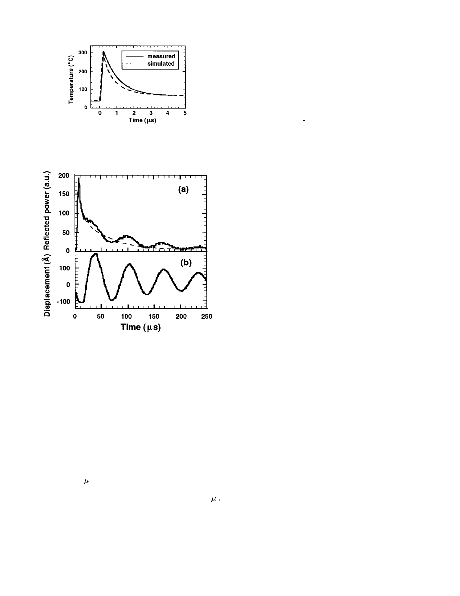
In one experiment, an 11-V 5- s heating pulse [Fig. 7(a)]
was applied across the Type-A heater. The instantaneous
current through the cantilever was determined from the voltage
across a 100-
series resistor, and the oscilloscope trace is
reproduced in Fig. 7(b). Knowing the voltage and current,
the heater resistance can be calculated at every point in time.
Because the cantilever legs have a much greater thermal mass
than the heater region, its temperature excursions are small in
comparison, and therefore changes in its electrical resistance
introduce only a slight error into the calculations, below 5%
in this case.
To be able to continue monitoring the heater resistance after
the voltage pulse has elapsed, a constant 1-V dc offset was
applied. The value of 1 V was chosen to avoid significant
self-heating. The calculated heater resistance during and after
the heating pulse was converted to a temperature scale based
on the heater’s previously measured temperature coefficient
of resistance. The derived heater temperature is shown in
Fig. 7(c). It is seen the heating pulse caused the heater
temperature to rise to approximately 200 C [Fig. 7(c), solid
line]. Afterwards, the heater cooled toward room temperature
Authorized licensed use limited to: Politechnika Slaska. Downloaded on May 29, 2009 at 04:22 from IEEE Xplore. Restrictions apply.

CHUI et al.: CANTILEVERS WITH HEATERS AND SENSORS FOR DATA STORAGE
73
TABLE II
ANSYS F
INITE
-E
LEMENT
A
NALYSIS
P
ARAMETERS
. N
OTE
T
HE
U
SE OF
T
EMPERATURE
-D
EPENDENT
M
ATERIAL
P
ROPERTIES
(T
HERMAL
C
ONDUCTIVITY
, S
PECIFIC
H
EAT
,
AND
E
LECTRICAL
R
ESISTIVITY
)
Fig. 7.
Electrical measurements for estimating Type-A heater temperature
during and after a heating pulse. (a) Applied voltage pulse (amplitude is 12
V at time 0–5
s and 1 V at all other times). (b) Measured current using a
100-
sense resistor. (c) Derived heater temperature showing a thermal time
constant of approximately 10
s:
with a thermal time constant of about 10
s compared with
350–450
s for a commercial silicon cantilever without a
localized heater [25].
The thermal time constant of Type-B heaters was measured
using a similar electrical method. In this case, a 10-V 0.2-
s pulse was applied, and the result is shown in Fig. 8. It
is seen that the time constant for a 100- m-long cantilever
is approximately 0.8
s, one order of magnitude better than
for Type-A heaters. This is due to several reasons. First, the
Type-B geometry has shorter, wider legs, which form a better
thermal connection between the heater region and the base.
Second, the legs are phosphorus doped to higher conductivity,
allowing electrical power to be delivered more efficiently to
the heater and shorter heating pulses to be used. A shorter
heating pulse allows less time for the heat to diffuse from
the heater region to the surrounding silicon. The total heat-
affected volume is reduced and therefore easier to cool. Third,
the heater is now located in a constriction, which has a smaller
thermal mass that can be heated and cooled more efficiently.
VI. F
INITE
-E
LEMENT
A
NALYSIS
Finite-element analysis with ANSYS software was per-
formed to corroborate the experimental measurements on the
Type-A and Type-B heaters. The cantilever was represented
by a thermal/electrical finite-element model. Standard values
of silicon thermophysical properties [26] were used except
for thermal conductivity values, which were adjusted down
to reflect an experimentally observed reduction due to heavy
doping [27], [28], especially in thin silicon films [29]. (At-
tempts are being made to understand this phenomenon more
fully [30].) The variation of thermal conductivity and heat
capacity with temperature was represented by a temperature-
dependent property table in ANSYS. Two different sets of
material properties were defined, one for the heavily doped
cantilever legs and another for the more lightly doped heater
region.
To reduce simulation time without sacrificing accuracy, a
variable mesh size was used for the finite-element model,
with the mesh being finest around the heater region where the
temperature gradient was expected to be steepest. Variable time
steps were also used to reduce simulation time. The smallest
time steps were used at the beginning of the simulation period,
when the temperature was expected to be changing most
rapidly due to the heating pulse. The simulation parameters
are listed in Table II.
The actual ANSYS simulation was performed as a transient
analysis in which a voltage pulse was applied to the finite-
element model, and the temperature rise at the heater region
was calculated at specified time intervals. The simulated
results, shown by the dotted line in Fig. 7(c) (for the Type-A
heater) and Fig. 8 (for the Type-B heater), agree closely with
experiment.
VII. L
ASER
T
HERMOMETRY AND
V
IBROMETRY
M
EASUREMENTS
A supplementary type of measurement laser thermometry
was used to corroborate the electrical measurements of the
Authorized licensed use limited to: Politechnika Slaska. Downloaded on May 29, 2009 at 04:22 from IEEE Xplore. Restrictions apply.
74
JOURNAL OF MICROELECTROMECHANICAL SYSTEMS, VOL. 7, NO. 1, MARCH 1998
Fig. 8.
Time-domain temperature variation of Type-B heater subjected to
single heating pulse. The measured thermal time constant is approximately
0.8
s, representing an order-of-magnitude improvement over Type-A heaters.
The dotted line shows finite-element simulation data obtained with ANSYS.
Fig. 9.
(a) Reflected laser power from Type-A heater subjected to heating
pulse: the dotted line represents the estimated reflectivity curve without
mechanical vibration. (b) Laser vibrometer output signal showing mechanical
vibration of cantilever tip.
heaters’ thermal behavior. Laser thermometry relies on the
fact that the optical reflectance of most materials varies with
temperature. While this type of measurement is commonly
used with metals with up to picosecond-level resolution, in
some cases it has been adapted for investigating semiconductor
devices [31] such as SOI power transistors [32]. In our
experimental setup, a low-power laser beam is focused on
a heater-cantilever, and the reflected power is measured at
different points in time. The results are used to estimate the
heater temperature and the thermal time constant.
Fig. 9 shows the reflected laser power from a location near
the tip of a 200- m-long Type-A cantilever in response to a
heating pulse. This curve shows two distinct phenomena: an
oscillation at 14 kHz and a decay time on the order of 10
s
The overall decay is believed to be related to the cantilever’s
temperature coefficient of reflectivity; the time constant for this
decay is consistent with the electrical resistance measurements.
In addition, the oscillation is believed to be due to a thermally
induced vibration. Since the cantilever has a 1000- ˚
A oxide
layer, it is expected to show differential thermal expansion
when heated.
To confirm this hypothesis, we used a laser vibrometer
[33] to study the pure mechanical behavior of a cantilever
in response to a heating pulse. In this technique, a laser
interferometer is used to measure the motion of the cantilever
tip with angstrom-level resolution. The output of the vibrom-
eter is shown in Fig. 9. A decaying sinusoidal oscillation is
observed, confirming the mechanical origins of the oscillation
in Fig. 9. From Fig. 9(b), the initial amplitude of the vibration
is estimated at 300 ˚
A It should be pointed out that our
measurement of heat-induced mechanical oscillation in the
cantilevers does not imply a limitation to their use in data
storage. In operation, the cantilevers are placed in continuous
contact with the polycarbonate substrate, and the heat pulses do
not cause sufficient mechanical oscillation for loss of contact
to occur.
As supplementary techniques to electrical measurements,
laser thermometry and vibrometry make it possible to char-
acterize cantilever behavior in detail. Laser thermometry can
provide spatially and temporally resolved measurements of
cantilever temperature; laser vibrometry can do the same for
cantilever motion. These two types of measurement will be
useful for developing improved cantilevers for thermomechan-
ical data storage and other applications.
VIII. F
REQUENCY
-D
OMAIN
T
HERMAL
A
NALYSIS
The time-domain electrical resistance measurements de-
scribed above revealed only one of the characteristic time
constants of the cantilever. It is possible that longer secondary
time constants exist that were not readily observable due to
the short time scales used in the measurements. To further
understand the relationship between thermal time constants
and cantilever geometry, a frequency-domain measurement of
a Type-B heater was performed.
In this thermal analysis, a 1.5-V dc signal with a 0.1-V ac
component was applied across a Type-B cantilever. An HP
89410 vector analyzer was used to measure the input voltage
and the current through the heater (via a series sensing resistor)
and to calculate the resulting resistance in real time. This
resistance is expected to vary at the same frequency as the ac
component of the applied voltage, since the electrical power
supply to the heater varies at that frequency. The variation in
the resistance of the heater is therefore an indication of its
thermal fluctuation. By repeating the measurement at various
frequencies between 100 Hz to 1 MHz, a thermal response
profile can be obtained for the heater.
Certain general predictions can be made about the frequency
response. When the frequency of the ac component is low, the
heater temperature is expected to be able to fully follow the
variation in the electrical power supply. This is because the
heater region (i.e., the tip of the cantilever) can essentially
equilibrate itself with the remainder of the structure (i.e.,
the constriction, the legs and the base) at every point in
time by virtue of heat conduction through the cantilever.
At higher frequencies, however, the fluctuation in heater
temperature will decrease in amplitude because heat diffusion
along the cantilever legs is not rapid enough to allow full
thermal equalization between the constriction and the base. At
Authorized licensed use limited to: Politechnika Slaska. Downloaded on May 29, 2009 at 04:22 from IEEE Xplore. Restrictions apply.

CHUI et al.: CANTILEVERS WITH HEATERS AND SENSORS FOR DATA STORAGE
75
(a)
(b)
Fig. 10.
(a) Frequency-dependent temperature fluctuation of Type-B heater
subjected to sinusoidally varying-input power. The higher the frequency
of variation, the smaller the thermal fluctuation. Note the pole at 1 kHz
(corresponding to the time constant of the cantilever legs) and a less dis-
tinct one around 100 kHz (corresponding to that of the heater constric-
tion). The 0-dB point on the
y axis is arbitrary. (b) Capacitor-resistor
thermodynamic model based on the cantilever’s geometry and material
properties. The output signal is measured at point V. Component val-
ues:
R1 = 12 000 K/W; C1 = 0:6 nJ/K; R2 = 6000 K/W; and
C2 = 0:01 nJ/K:
even higher frequencies, the constriction itself cannot support
adequate heat exchange between the heater and the legs, so
the heater temperature will remain nearly constant.
This prediction is confirmed by the experimental results
shown in Fig. 10(a). At low frequencies the temperature
fluctuation of the heater is largely constant, but beyond 1 kHz
the amplitude of fluctuation decays rapidly with frequency,
with an accelerated rate of decay occurring above 100 kHz.
Of special interest is the pole on the graph at 1 kHz. This pole
corresponds to a “slow” time constant of about 150
s and is
believed to be associated with the cantilever legs. This “slow”
time constant was not readily observable from the electrical
resistance measurements of Fig. 8.
For calibration purposes, the measurement was also per-
formed on a carbon-film resistor, which undergoes no ap-
preciable heating, and in this case essentially no apparent
resistance variation was observed except at frequencies ap-
proaching 1 MHz. This variation is believed to be associated
with signal distortion in the measurement circuitry rather than
the device under test, and the data in Fig. 10 has been adjusted
to account for this effect.
To verify the results of the frequency-domain analysis, we
analyzed the Type-B heater in SPICE using a thermodynamic
model based on the thermal resistances and capacitances of the
(a)
(b)
Fig. 11.
Atomic-force microscopy image of sample data tracks written with
(a) Type-A heater using 16-V 20-
s pulses with a period of 90–200 s (about
10 kb/s). (b) Type-B heater using 30-V 0.2-
s pulses with a period of 7–14
s (about 100 kb/s).
cantilever. These values were calculated based on the actual
dimensions of the cantilever and the thermal conductivity
and heat capacity of silicon. The distributed nature of the
thermal resistances and capacitances was accounted for by
using multiple resistor and capacitor elements to represent each
of two sections of the cantilever (the leg and the constriction).
The heating element was modeled with an ac current source at
the heater tip [see Fig. 10(b)]. Using this model, a simulated
frequency response was obtained in good agreement with the
measured response. This result shows that it is indeed possible
to generate an accurate thermodynamic model for the heater-
cantilever based on its dimensions and material properties.
This type of thermodynamic modeling will prove useful for
designing future devices.
IX. T
HERMAL
W
RITING
E
XPERIMENTS
Basic functionality of the heaters have been demonstrated,
as shown by the AFM micrograph in Fig. 11. Sample data
tracks were written with the heater on a rotating polycarbonate
sample. The writing was very reliable, and different-sized
marks could be written by varying the pulse conditions.
The smallest marks in Fig. 11 correspond to bit densities
approaching 10 Gb/in , assuming a standard (2,7) code. Since
this experiment was aimed at comparing the writing speeds
of Type-A and Type-B heaters, the test conditions were not
necessarily optimized to produce the maximum bit density.
Authorized licensed use limited to: Politechnika Slaska. Downloaded on May 29, 2009 at 04:22 from IEEE Xplore. Restrictions apply.
76
JOURNAL OF MICROELECTROMECHANICAL SYSTEMS, VOL. 7, NO. 1, MARCH 1998
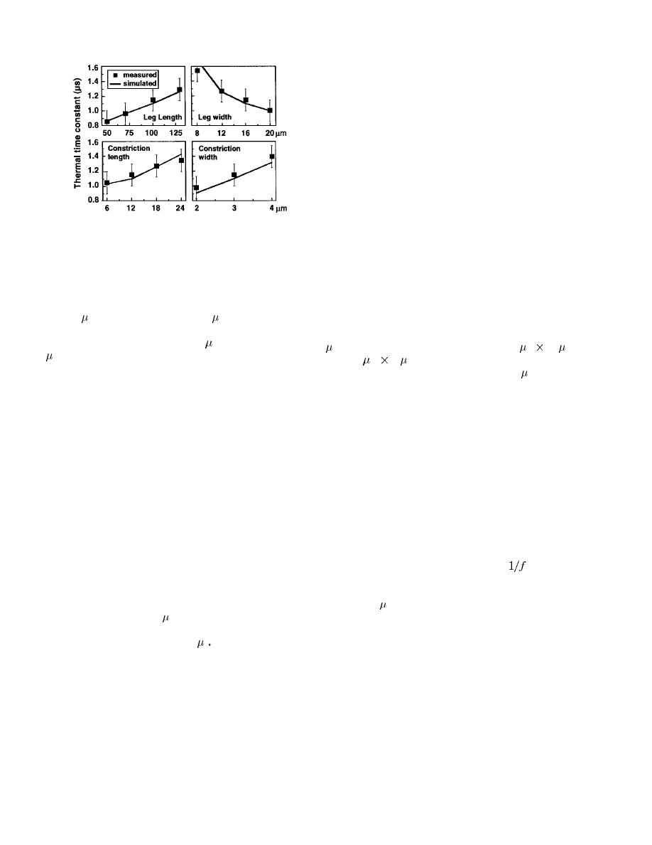
Fig. 12.
Measured and simulated thermal time constants for families of
Type-B heaters under repeated-pulse conditions. In general, it is seen that
shorter wider legs and smaller heater constrictions give rise to shorter time
constants. The “nominal” cantilever geometry from which variants are derived
[see Fig. 6(b)] has dimensions 100
2 16 2 1 m (for each leg) and
12
2 3 2 1 m (for the constriction).
With Type-A heaters, typical pulse parameters were 16 V
and 20
s with a period of 90–200
s, implying a writing
speed of approximately 10 kb/s. With Type-B heaters, the
pulse parameters were 30 V and 0.2
s with a period of 7–14
s, implying a writing speed of approximately 100 kb/s, or a
tenfold improvement.
X. H
EATER
D
ESIGN
O
PTIMIZATION
In an attempt to find the optimal heater design and to show
that the cantilever behavior is understandable and predictable,
families of Type-B cantilevers with different geometric config-
urations were fabricated and tested. Finite-element simulations
were also performed for comparison. The measured and simu-
lated thermal time constants are shown in Fig. 12. Cantilever
dimensions being varied include the length and width of the
cantilever legs as well as the length and width of the heater
constriction.
The measurements were performed with repeated heating
pulses rather than isolated ones, since the former condition
more closely resembles actual operation. In this case, the ther-
mal time constant is expected to differ from the isolated-pulse
scenario because the cantilever assumes a pseudosteady-state
temperature profile in which the legs experience appreciable
heating. For the Type-B cantilever measured earlier, which
had a time constant of 0.8
s under isolated-pulse conditions,
it was found that under repeated-pulse conditions the time
constant increased slightly to 1.2
s This can be attributed
to the reduced heat-sinking capability of the legs, which were
at an elevated temperature. ANSYS modeling of this scenario
confirmed the slight increase in time constant and the elevated
temperature profile of the legs.
Measurements on the families of Type-B cantilevers
showed, not surprisingly, that the time constant decreases
with decreasing constriction length, decreasing leg length,
increasing leg width, and decreasing constriction width. The
first three trends can be explained by the fact that a smaller
thermal resistance from the heater (the cantilever tip) to the
heat sink (the cantilever base) is present when the constriction
is shorter and the legs are shorter and wider. The last trend
is most likely due to the fact that the smaller thermal mass
associated with a narrower constriction can be heated and
cooled more efficiently—this effect apparently more than
offsets the reduced conductivity of the constriction itself.
From the measured data, it is seen that the optimal heater
design calls for as short and wide legs as possible and
as short and narrow a heater constriction as possible. This
rule is obviously subject to practical constraints imposed
by fabrication technology, mechanical robustness, and, most
importantly, the data-storage system itself. For example, the
constriction cannot be made too narrow or the cantilever
may break too easily. In addition, the heater region cannot
be made too small, in which case its electrical resistance
is overwhelmed by that of the legs, making it difficult to
deliver power to the heater itself. Most importantly, the
cantilever cannot be made too short and too wide, otherwise,
its spring constant exceeds the limit for wear-free operation on
polycarbonate substrates (approximately 1 N/m in this case).
An effective way of reducing the thermal time constant is
to use thinner cantilevers, since this allows shorter and wider
legs to be used without increasing the spring constant. For
example, given a required spring constant of 1 N/m, a 0.34-
m-thick cantilever can be designed with 40
m
16- m legs
and a 4
m
2- m constriction. This cantilever is expected
to have a thermal time constant below 0.5
s, according to
ANSYS modeling.
XI. C
ONCLUSIONS
In this report, we have described two novel capabilities
of AFM cantilevers. First, we have added built-in sensing
functionality onto low-stiffness cantilevers with integrated tips.
A new process was developed that allows for considerably
thinner piezoresistive cantilevers than previously possible, and
the process is scalable to even thinner cantilevers. Measured
sensitivity is in agreement with predictions, so that we can
calculate with confidence the type of cantilever needed to
achieve a given level of performance. The current cantilevers
are adequate for detecting 100–200- ˚
A-deep features in a 100-
kHz bandwidth. They also show excellent
noise behavior.
A heater process was developed on separate cantilevers to
allow thermal writing without a laser. Thermal time constants
as low as 1
s were achieved with the appropriate cantilever
geometry and doping method. Systematic measurement and
simulation of different families of cantilevers enabled us to
predict an optimized heater design. The accuracy of ANSYS-
based finite-element analysis and SPICE simulations was
established by virtue of their close agreement with experiment.
Furthermore, a thermodynamic model based on the cantilevers
material properties proved to be a valuable tool for understand-
ing the thermal behavior of the device. Taken together, these
measurement and simulation techniques form a reliable design
methodology for future micromachined heaters.
Possibilities for future improvement in AFM thermome-
chanical data storage include the fabrication of combined
read/write devices based on the separately optimized piezore-
sistive cantilevers and resistive heaters described in this article.
Another area of improvement is the use of cantilever arrays
Authorized licensed use limited to: Politechnika Slaska. Downloaded on May 29, 2009 at 04:22 from IEEE Xplore. Restrictions apply.

CHUI et al.: CANTILEVERS WITH HEATERS AND SENSORS FOR DATA STORAGE
77
to raise the data throughput. Simultaneous readback with two
piezoresistive cantilevers has already been demonstrated, as
shown in Fig. 5. Furthermore, the operation of cantilevers
in parallel has also been reported in AFM microscopy [34]
and nanolithography [35]. One of the advantages of microma-
chining is that the components are batch fabricated, so that
arrays of tips can be easily made. We have been routinely
able to fabricate arrays of four cantilevers with high yield,
and believe that even larger arrays are possible. Ultimately,
parallel operation may prove to be a very effective way of
improving the level of performance of AFM thermomechanical
data storage.
A
CKNOWLEDGMENT
We would like to thank C. F. Quate, S. C. Minne, and H. T.
Soh of Stanford for sharing their expertise in AFM cantilever
technology and J. D. Plummer of Stanford and L. S. Fan of
IBM for their insight on heater behavior. We are also grateful
to M. Tortonese of Park Scientific Instruments for helpful
discussions and to O. W. K¨ading for his help with the laser
thermometry setup.
R
EFERENCES
[1] T. R. Albrecht, S. Akamine, T. E. Carver, and C. F. Quate, “Microfab-
rication of cantilever styli for the atomic force microscope,” J. Vac. Sci.
Technol., vol. 8, pp. 3386–3396, 1990.
[2] J. Brugger, R. A. Buser, and N. F. de Rooij, “Silicon cantilevers and
tips for scanning force microscopy,” Sens. Actuators A, vol. 34, pp.
193–200, 1992.
[3] O. Wolter, Th. Bayer, and J. Greschner, “Micromachined silicon sensors
for scanning force microscopy,” J. Vac. Sci. Technol. B, vol. 9, pp.
1353–1357, 1991.
[4] A. Majumdar, P. I. Oden, J. P. Carrejo, L. A. Nagahara, J. J. Graham,
and J. Alexander, “Nanometer-scale lithography using the atomic force
microscope,” Appl. Phys. Lett., vol. 6, pp. 2293–2295, 1992.
[5] E. S. Snow and P. M. Campbell, “Fabrication of Si nanostructures with
an atomic force microscope,” Appl. Phys. Lett., vol. 64, pp. 1932–1934,
1994.
[6] S. C. Minne, H. T. Soh, P. Flueckiger, and C. F. Quate, “Fabrication
of 0.1
m metal oxide semiconductor field-effect transistors with the
atomic force microscope,” Appl. Phys. Lett., vol. 66, pp. 703–705, 1995.
[7] H. J. Mamin, B. D. Terris, L. S. Fan, S. Hoen, R. C. Barrett, and D.
Rugar, “High-density data storage using proximal probe techniques,”
IBM J. Res. Develop., vol. 39, pp. 681–699, 1995.
[8] R. Barrett and C. F. Quate, “Charge storage in a nitride-oxide-silicon
medium by scanning capacitance microscopy,” J. Appl. Phys., vol. 70,
pp. 2725–2733, 1991.
[9] S. Hosaka, H. Koyanagi, and A. Kikukawa,“Nanometer recording on
graphite and Si substrate using an atomic force microscope in air,” Jpn.
J. Phys., vol. 32, pp. L464–467, 1993.
[10] H. Kado and T. Tohda, “Nanometer-scale recording on chalcogenide
films with an atomic force microscope,” Appl. Phys. Lett., vol. 66, pp.
2961–2962, 1995.
[11] H. J. Mamin and D. Rugar, “Thermomechanical writing with an atomic
force microscope tip,” Appl. Phys. Lett., vol. 61, pp. 1003–1005, 1992.
[12] H. J. Mamin, L. S. Fan, S. Hoen, and D. Rugar, “Tip-based data storage
using micromechanical cantilevers,” Sens. Actuators A, vol. 48, pp.
215–219, 1994.
[13] S. Hoen, H. J. Mamin, and D. Rugar, “Thermomechanical data storage
using a fiber optic stylus,” Appl. Phys. Lett., vol. 64, pp. 267–269, 1994.
[14] M. Tortonese, R. C. Barrett, and C. F. Quate, “Atomic resolution with
an atomic force microscope using piezoresistive detection,” Appl. Phys.
Lett., vol. 62, pp. 834–836, 1993.
[15] M. Tortonese, Ph.D. dissertation, Stanford University, Stanford, CA,
1994.
[16]
, “Atomic force microscopy using a piezoresistive cantilever,” in
Proc. Transducers ’91, Int. Conf. Solid-state Sensors and Actuators, San
Francisco, CA, pp. 448–51.
[17] B. W. Chui, H. J. Mamin, B. D. Terris, T. D. Stowe, D. Rugar, and
T. W. Kenny, “Low-stiffness silicon cantilevers for thermal writing and
piezoresistive readback with the atomic force microscope,” Appl. Phys.
Lett., vol. 69, pp. 2767–2769, 1996.
[18] B. W. Chui, H. J. Mamin, B. D. Terris, R. P. Ried, D. Rugar, T. D.
Stowe, H. T. Soh, S. C. Minne, C. F. Quate, Y. S. Ju, K. E. Goodson,
and T. W. Kenny, “Improved cantilevers for AFM thermomechanical
data storage,” in Proc. Solid-State Sensor and Actuator Workshop, Hilton
Head, SC, June 2–6, 1996, pp. 219–224.
[19] IBIS Technology Corp., Danvers, MA 01923 USA.
[20] Solecon Laboratories, San Jose, CA 95131 USA.
[21] R. P. Ried, H. J. Mamin, B. D. Terris, L. S. Fan, and D. Rugar,
“6-MHz 2-N/m piezoresistive atomic-force-microscope cantilevers with
INCISIVE tips,” IEEE J. Microelectromech. Syst., vol. 6, no. 4, pp.
294–302, 1997.
[22] B. D. Terris, S. A. Rishton, H. J. Mamin, R. P. Ried, and D. Rugar,
“Atomic force microscope based data storage: Track servo and wear
study,” Appl. Phys. A, to be published.
[23] C. H. Mastrangelo, J. H.-J. Yeh, and R. S. Muller, “Electrical and optical
characteristics of vacuum-sealed polysilicon microlamps,” IEEE Trans.
Electron Devices, vol. 39, pp. 1363–75, 1992.
[24] J. H. Das and N. C. MacDonald, “Micromachined field emission
cathode with an integrated heater,” J. Vac. Sci. Technol. B, vol. 13, pp.
2432–2435, 1995.
[25] H. J. Mamin, “Thermal writing using a heated atomic force microscope
tip,” Appl. Phys. Lett., vol. 69, pp. 433–435, 1996.
[26] F. P. Incropera and D. P. de Witt, Fundamentals of Heat and Mass
Transfer, 3rd ed.
New York: Wiley, 1990, Appendix A1.
[27] G. A. Slack, “Thermal conductivity of pure and impure silicon, silicon
carbide, and diamond,” J. Appl. Phys., vol. 35, pp. 3460–3466, 1964.
[28] L. Weber and E. Gmelin, “Transport properties of silicon,” Appl. Phys.
A, vol. 53, pp. 136–140, 1991.
[29] M. Asheghi, M. N. Touzelbaev, Y. K. Leung, S. S. Wong, and K.
E. Goodson, “Temperature-dependent thermal conductivity of single-
crystal silicon layers in SOI substrates,” ASME J. Heat Transfer, vol.
120, pp. 1–7, 1998.
[30] M. Asheghi, B. W. Chui, T. W. Kenny, and K. E. Goodson, “Thermal
conduction in single-crystal silicon cantilevers,” to be published.
[31] P. W. Epperlein, “Micro-temperature measurements on semiconductor
laser mirrors by reflectance modulation: A newly developed technique
for laser characterization,” Jpn. J. Appl. Phys., vol. 32, pp. 5514–5522,
1993.
[32] Y. S. Ju, O. W. K¨ading, Y. K. Leung, S. S. Wong, and K. E. Goodson,
“Short-timescale thermal mapping of semiconductor devices,” IEEE
Electron Device Lett., vol. 18, pp. 169–171, 1997.
[33] Polytec Laser Vibrometer OVF-501-0, Polytec P. I., Inc., Costa Mesa,
CA.
[34] S. C. Minne, S. R. Manalis, and C. F. Quate, “Parallel atomic force
microscopy using cantilevers with integrated piezoresistive sensors
and integrated piezoelectric actuators,” Appl. Phys. Lett., vol. 67, pp.
3918–3920, 1995.
[35] S. C. Minne, S. R. Manalis, A. Atalar, and C. F. Quate, “Independent
parallel lithography using the atomic force microscope,” J. Vac. Technol.
B, vol. 14, pp. 2456–2459, 1996.
Benjamin W. Chui (S’97) received the B.S. and
M.S. degrees in electrical engineering from Stanford
University, Stanford, CA, in 1992. He is currently
working towards the Ph.D. degree at Stanford Uni-
versity.
He worked as an Integrated Circuit Design En-
gineer for three years. He is currently involved
in the fabrication and testing of silicon microcan-
tilevers for AFM thermomechanical data storage
in collaboration with the IBM Almaden Research
Center and the Stanford Microstructures and Sensors
Laboratory.
Mr. Chui received the Henry Ford III Award for highest academic achieve-
ment in the school of engineering and is a recipient of the IBM Cooperative
Fellowship.
Authorized licensed use limited to: Politechnika Slaska. Downloaded on May 29, 2009 at 04:22 from IEEE Xplore. Restrictions apply.

78
JOURNAL OF MICROELECTROMECHANICAL SYSTEMS, VOL. 7, NO. 1, MARCH 1998
Timothy D. Stowe received the B.S. degree in
applied physics from Cornell University, Ithaca,
NY, in 1993 and the M.S. degree in applied physics
from Stanford University, Stanford, CA, in 1995.
He is currently working toward the Ph.D. degree in
at Stanford University.
He is currently a John and Fannie Hertz Founda-
tion Fellow at Stanford University. He is a Member
of the Stanford Microstructures and Sensors Labo-
ratory and is working in collaboration with the IBM
Almaden Research Center on the fabrication and
testing of ultrathin cantilevers for nuclear magnetic resonance microscopy.
Yongho Sungtaek Ju received the B.S. degree from
Seoul National University, Seoul, Korea in 1993 and
the M.S. degree from Stanford University, Stanford,
CA in 1995, both in mechanical engineering. He
is currently working toward the Ph.D. degree at
Stanford University.
He is investigating short-timescale thermal be-
havior of microdevices and thermal phenomena in
nanostructures.
Mr. Ju is a recipient of the University Presidential
Award and the Alumni Association Award from
Seoul National University.
Kenneth E. Goodson received the B.S., M.S., and
Ph.D. degrees in mechanical engineering from the
Massachusetts Institute of Technology, Cambridge,
in 1989, 1991, and 1993, respectively.
He is an Assistant Professor and Terman Fellow
with the Department of Mechanical Engineering,
Stanford University, CA. For 16 months starting
in 1993, he was with Daimler-Benz AG, Germany,
where he worked on the application of CVD dia-
mond layers for the cooling of high-power automo-
tive electronics. He joined Stanford University in
1994, where he now supervises Ph.D. students studying thermal phenomena
in electronic micro and nanostructures.
Dr. Goodson’s dissertation research on the self-heating of SOI transistors
was recognized through the Best Student Paper Award at the 1992 IEEE
International Electron Devices Meeting. He is an ONR Young Investigator
and a recipient of the NSF CAREER Award.
Thomas W. Kenny received the B.S. degree in
physics from the University of Minnesota, Min-
neapolis, in 1983 and the M.S. and Ph.D. degrees in
physics from the University of California, Berkeley,
in 1987 and 1989, respectively.
He has worked at the Jet Propulsion Laboratory,
where his research focused on the development of
electron-tunneling-based high-resolution microsen-
sors. Since 1994, he has been Assistant Professor
and Terman Fellow with the Mechanical Engineer-
ing Department, Stanford University, Stanford, CA.
He currently oversees graduate students in the Stanford Microstructures and
Sensors Laboratory, whose research activities cover a variety of areas such as
advanced tunneling sensors, small student-built spacecraft, novel fabrication
techniques for micromechanical structures, and the study of nonclassical
phenomena within this context. In particular, his group is collaborating with
researchers from the IBM Almaden Research Center on nuclear magnetic
resonance microscopy as well as AFM thermomechanical data storage.
H. Jonathon Mamin received the B.S. degree in
physics from Stanford University, Stanford, CA,
in 1978 and the Ph.D. degree in physics from the
University of California, Berkeley, in 1984.
After receiving the Ph.D. degree, he remained
at Berkeley as a Postdoctoral Fellow in the then-
emerging field of scanning-tunneling microscopy.
Since 1987, he has been a Research Staff Member
at the Almaden Research Center, IBM Research
Division, San Jose, CA. His research interests in-
clude magnetic-force microscopy, surface modifica-
tion with scanning probes, and high-density data storage.
Dr. Mamin is a Member of the American Physical Society and a Board
Member of the Nanometer Scale Science.
Bruce D. Terris received the B.S. degree in applied
physics from Columbia University, NY, in 1979 and
the M.S. and Ph.D. degrees in physics from the
University of Illinois, Urbana-Champaign, in 1981
and 1983, respectively.
After receiving the Ph.D. degree, he was a Post-
doctoral Fellow at the Argonne National Labo-
ratory. Since 1985, he has been a research staff
member at the Almaden Research Center, IBM
Research Division, San Jose, CA. His research inter-
ests have included thin-film superconductivity and
magnetism, contact electrification of insulators, and new types of scanning-
probe microscopes (STM, AFM, near-field optical, etc.). His recent research
has focused on the application of proximal probe techniques to high-density
data storage.
Dr. Terris is a Member of the American Physical Society.
Robert P. Ried (S’87–M’95) received the B.S.
degree from Rice University, Houston, TX, in 1984,
the M.Eng. degree from Cornell University, Ithaca,
NY, in 1985, and the Ph.D. degree from the Uni-
versity of California, Berkeley, in 1994.
From 1985 to 1987, he was with AT&T Bell
Laboratories, Holmdel, NJ, as a Designer of long-
distance fiber-optic transmissions systems. He is
presently a Postdoctoral Researcher at the Almaden
Research Center, IBM Research Division, San Jose,
CA. His MEMS research projects have focused on
micromachined microphones and scanning-probe data storage.
Daniel Rugar (M’87) received the B.A. degree in
physics (magna cum laude) from Pomona College,
Claremont, CA, in 1975 and the Ph.D. degree in
applied physics from Stanford University, Stanford,
CA, in 1982.
From 1982 to 1984, he was the Hunt Fellow of
the Acoustical Society of America and a Reseach
Associate at Stanford University, where he worked
on acoustic microscopy and phonon dispersion in
superfluid helium. He joined the IBM Research
Division, San Jose, CA, in 1984 and has worked on
many aspects of high-density data storage and scanning-probe microscopy. His
present position is Manager of nanoscale studies. His current research interests
include new techniques for ultrahigh-density data storage, magnetic resonance-
force microscopy, and ultrasensitive force detection. He has published over
80 papers and holds 13 patents.
Dr. Rugar is a Member of the American Physical Society.
Authorized licensed use limited to: Politechnika Slaska. Downloaded on May 29, 2009 at 04:22 from IEEE Xplore. Restrictions apply.
Wyszukiwarka
Podobne podstrony:
A high sensitive piezoresistive sensor for stress measurements
A Technique to Measure Eyelid Pressure using Piezoresistive Sensors
piezoresistive sensor rosettes
Force Measurements In A Scanning Force Microscope With Piezoresistive Sensors
Measuring the deflection of a micromachined cantilever in cantilever device using a piezoresistive s
A Low Cost Integrated Approach for Balancing an Array of Piezoresistive Sensors
SI – Sensory Integration
sensoryka wrażliwość czuciowa
integracja sensoryczna5 id 2181 Nieznany
Terapia Integracji Sensorycznej Opr, metody pracy
POMIAR DŁUGOŚCI I OBWODÓW KOŃCZYN GÓRNYCH I DOLNYCH, utp, Sensory i pomiary wielkości nieelektryczny
Terapia dzieci z sensoryzmami, Autyzm
Piezorezystancyjny czujnik ciśnienia w kolektorze dolotowym (2)
Wprowadzenie do teorii integracji sensorycznej
Co to jest integracja sensoryczna
d7067240 7846 11dc a67c 0019bbdf5d02 Proximity sensor capactivite
Analiza sensoryczna produktu projekt id 61348 (2)
sensoryka laborki, MGR, sem I, Analiza sensoryczna
więcej podobnych podstron