DISCONTINUED PRODUCT
— FOR REFERENCE ONLY
Designed specifically to meet the requirement for extended opera-
tion of battery-powered equipment such as cordless and cellular tele-
phones, the A8205SLH voltage regulators offer the reduced dropout
voltage and quiescent current essential for maximum battery life.
Applicable also to palmtop computers and personal data assistants,
these devices deliver a regulated output at up to 200 mA (transient),
which is limited only by package power dissipation. Regulated output
voltages of 2.7, 2.8, 3.0, 3.3, 3.6, 4.0, and 5.0 V are currently provided.
Other voltages, down to 2.0 volts, are available on special order.
A PMOS pass element provides a typical dropout voltage of only
75 mV at 100 mA of load current. The low dropout voltage permits
deeper battery discharge before output regulation is lost. Quiescent
current does not increase significantly as the dropout voltage is ap-
proached, an ideal feature in standby/resume power systems where data
integrity is crucial. Regulator accuracy and excellent temperature
characteristics are provided by a bandgap reference. The A8205SLH
includes an ENABLE input to give the designer complete control over
power up, standby, or power down.
These devices are supplied in a thermally enhanced 5-lead small-
outline plastic package similar to the SOT-23, and fitting the SC-74A
footprint. All devices are rated for operation over a temperature range
of -20
°C to +85°C.
FEATURES AND BENEFITS
■ High Efficiency Provides Extended Battery Life
■ 75 mV Typical Dropout Voltage at I
O
= 100 mA
■ 55 µA Typical Quiescent Current
Less Than 1
µA “Sleep” Current
■ Low Output Noise
■ 200 mA Peak Output Current
■ Improved PSRR and Transient Performance
APPLICATIONS
■ Cordless and Cellular Telephones
■ Personal Data Assistants
■ Personal Communicators
■ Palmtop Computers
LOW-DROPOUT REGULATORS
— HIGH EFFICIENCY
Data Sheet
27468.20
Always order by complete part number, e.g., A8205SLH-xx , where “xx”
is the required output voltage in tenths or “ADJ” for adjustable.
ABSOLUTE MAXIMUM RATINGS
Input Voltage, V
I
. . . . . . . . . . . . . . . 7 V
Peak Output Current,
I
OM
. . . . . . . . . . . . . . . . . . 200 mA*
Enable Input Voltage, V
E
. . . . . . . . . . V
I
Operating Temperature Range,
T
A
. . . . . . . . . . . . . -20
°
C to +85
°
C
Junction Temperature, T
J
. . . . +150
°
C
Storage Temperature Range,
T
S
. . . . . . . . . . . . -40
°
C to +150
°
C
* Output current rating is limited by input
voltage, duty cycle, and ambient temperature.
Under any set of conditions, do not exceed a
junction temperature of +150
°C. See follow-
ing pages.
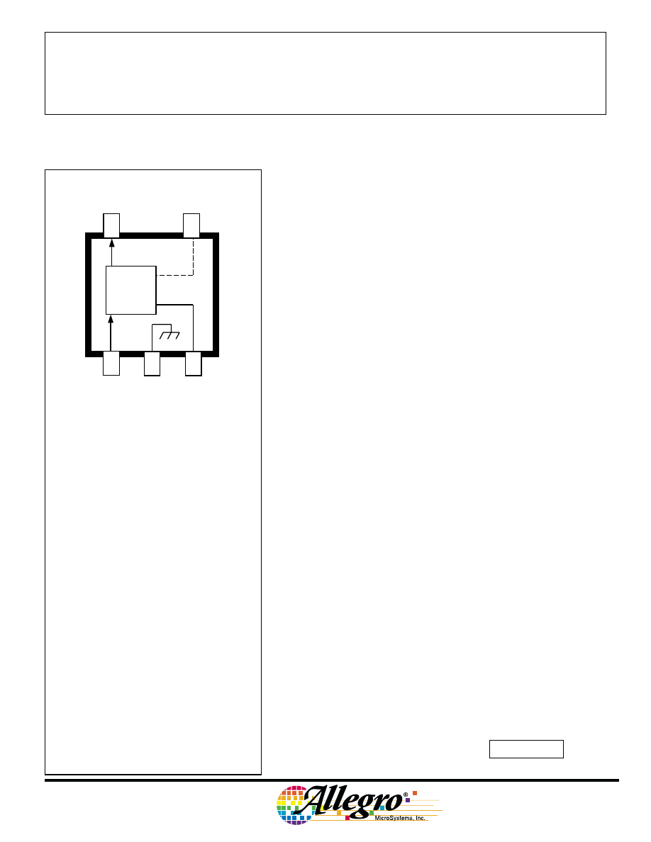
8205
Dwg. PS-021-5
VR
2
GND
3
NC
OR
ADJ*
1
ENABLE
5
IN
OUT
4
*NO CONNECTION (fixed regulators) or
ADJUST (A8205SLH-ADJ only).
PRELIMINARY INFORMATION
(subject to change without notice)
December 6, 1999
8205
LOW-DROPOUT
REGULATORS
115 Northeast Cutoff, Box 15036
Worcester, Massachusetts 01615-0036 (508) 853-5000
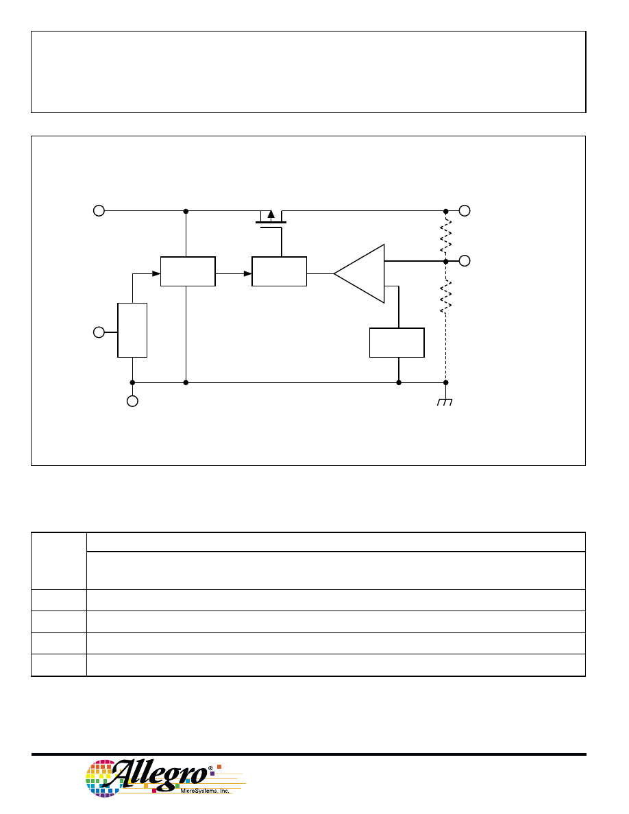
FUNCTIONAL BLOCK DIAGRAM
Copyright © 1999, 2000 Allegro MicroSystems, Inc.
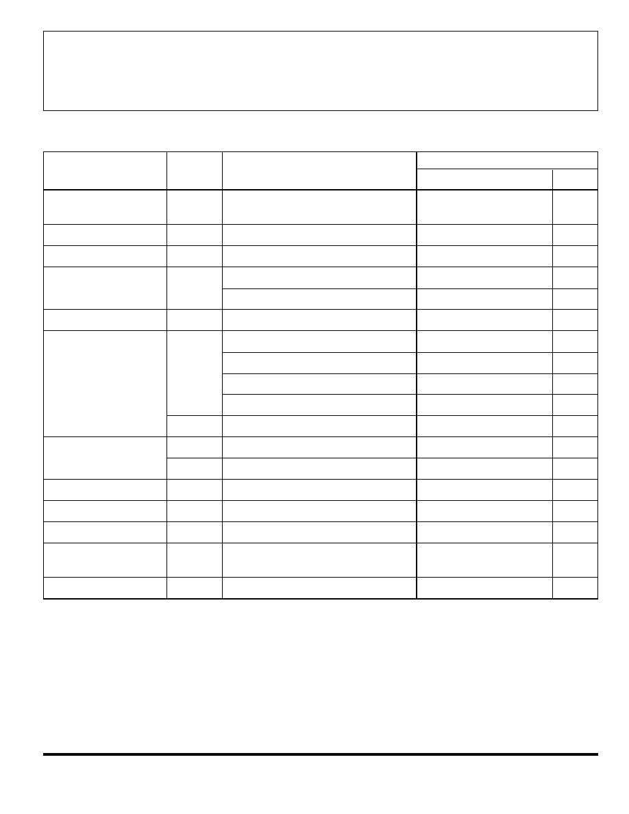
A8205SLH Maximum Allowable Average Output Current* with device mounted on 2.24" x 2.24"
(56.9 mm x 56.9 mm) solder-coated copper-clad board in still air.
Allowable Total Average (10 ms) Output Current in Milliamperes with T
J
= 150
°C, Duty Cycle = 100%†
V
I
- V
O
T
A
0.5
1.0
1.5
2.0
2.5
3.0
3.5
4.0*
4.5*
25
°C
200
200
200
200
200
189
162
142
126
50
°C
200
200
200
200
182
152
130
114
101
70
°C
200
200
200
182
145
121
104
91
81
85
°C
200
200
197
148
118
98
84
74
66
* Absolute maximum peak output current rating is 200 mA; absolute maximum input voltage is 7 V.
† I
O
= (T
J
– T
A
)/([V
I
– V
O
] R
θJA
x dc) = (150 – T
A
)/([V
I
– V
O
] x 220 x 1.00)
Output current rating can be increased (to 200 mA maximum) by additional heat sinking or reducing the duty cycle.
DRIVE
BANDGAP
REF.
ERROR
AMP
Dwg. FS-012-6
BIAS
ENABLE
IN
ENABLE
OUT
1
5
3
2
GND
ADJUST
(SUFFIX "-ADJ" ONLY)
OTHERWISE
NO CONNECTION
(FIXED REG'S)
4
8205
LOW-DROPOUT
REGULATORS
www.allegromicro.com
ELECTRICAL CHARACTERISTICS at T
A
= +25
°C, V
E
= V
I
(unless otherwise noted).
Limits
Characteristic
Symbol
Test Conditions
Min.
Typ.
Max.
Units
Output Voltage
V
O
V
I
≥ V
O(nom)
+ 1 V, 1 mA
≤ I
O
≤ 150 mA*,
reference specified V
O(nom)
—
0.0
±1.5
%
Output Volt. Temp. Coeff.
a
VO
V
I
= 6 V, I
O
= 10 mA, T
J
≤ 125°C
—
40
—
ppm/
°C
Line Regulation
∆V
O(
∆VI)
V
O(nom)
+ 1 V
≤ V
I
≤ 7 V, I
O
= 3 mA
—
—
±1.5
%
Load Regulation
∆V
O(
∆IO)
V
I
= V
O(nom)
+ 1 V, 1 mA
≤ I
O
≤ 150 mA*
—
—
±1.5
%
V
I
= 7 V, 1 mA
≤ I
O
≤ 150 mA*
—
—
±1.5
%
Dropout Voltage
V
I
min - V
O
I
O
= 100 mA
—
75
200
mV
Ground Terminal Current
I
GND
V
I
= V
O(nom)
+ 1 V, I
O
= 1 mA
—
55
65
µA
V
I
= V
O(nom)
+ 1 V, I
O
= 150 mA*
—
55
65
µA
V
I
= 7 V, I
O
= 1 mA
—
55
65
µA
V
I
= 7 V, I
O
= 150 mA*
—
55
65
µA
I
Q
V
I
≤ 7 V, V
E
≤ 0.8 V, I
O
= 0 mA
—
—
1.0
µA
ENABLE Input Voltage
V
EH
V
I
≥ V
O(nom)
+ 1 V, Output ON
2.0
—
—
V
V
EL
V
I
≥ V
O(nom)
+ 1 V, Output OFF
—
—
0.4
V
ENABLE Input Current
I
E
V
E
= V
I
= 7 V
—
—
±1.0
µA
Internal Reference Voltage
V
REF
—
1.26
—
V
ADJUST Input Current
I
ADJ
A8205SLH-ADJ only
—
0.10
—
µA
Rejection Ratio
PSRR
V
I
= V
O(nom)
+ 1.5 V, V
i
= 100 mV,
I
O
= 30 mA, f = 60 Hz
—
70
—
dB
Output Noise
e
n
10 Hz
≤ f ≤ 100 kHz, I
O
= 10 mA, C
O
= 10
µF
—
0.5
—
µV/√Hz
Typical values are at T
A
= +25
°C and are given for circuit design information only.
* Pulse test (
≤20 ms). See previous page for duty cycle limitations.
8205
LOW-DROPOUT
REGULATORS
115 Northeast Cutoff, Box 15036
Worcester, Massachusetts 01615-0036 (508) 853-5000
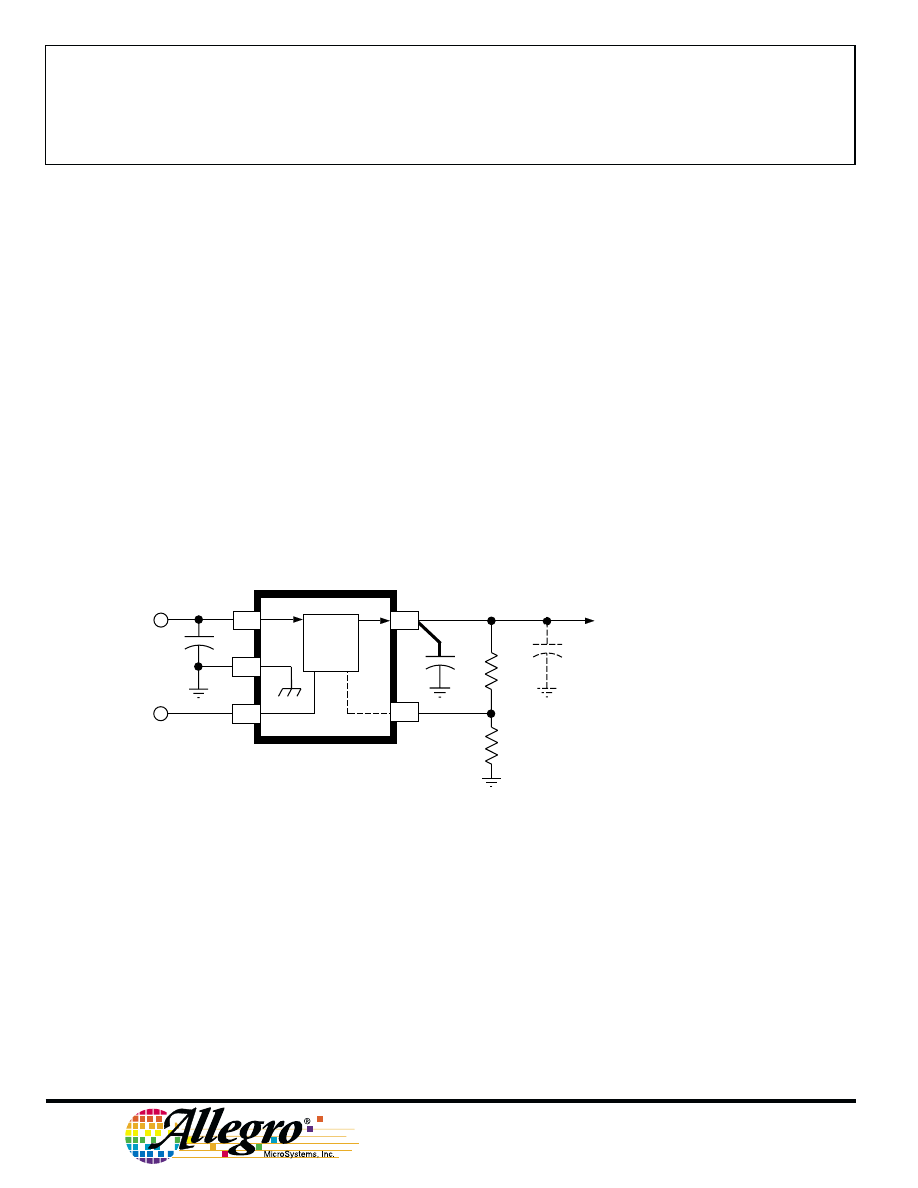
APPLICATIONS INFORMATION
Linear regulators require input and output capacitors in order to
maintain over-all loop stability. The recommended minimum
value for the input capacitor is 0.1
µF. The output capacitor is
the dominant pole that provides the high-frequency compensa-
tion required for over-all regulator loop stability. These devices
are stable with as little as 1
µF. However, to ensure stable
operation under all conditions and capacitor types, the recom-
mended minimum value is 4.7
µF. The output capacitor may be
partially distributed through the load circuits. However, at least
1
µF should be connected at the regulator using the shortest and
widest foil pattern possible.
The A8205SLH-ADJ requires an external voltage divider to set
up the desired regulated output voltage between 2.0 V and 6.8 V
(V
I
≤ 7 V). The two resistors are chosen such that
V
O
= 1.26 (R
1
+ R
2
)/R
2
.
The resistor values are usually as high as possible to maintain
high circuit efficiency, but R
2
should be less than 300 k
Ω.
Dwg. ES-015
ENABLE
(ACTIVE HIGH)
INPUT
(7.0 V MAX)
OUTPUT (2.0 V TO 6.8 V)
0.1
µF
(MIN)
1
µF
(MIN)
R1
R2
(300 k
Ω MAX)
VR
2
3
1
5
4
Thermal Considerations
These devices are intended to provide more than 150 mA of
continuous current in a very small package. The table on page 2
of this data sheet gives the maximum allowable average output
current for a worst-case printed circuit design (R
θJA
= 220
°C/W
with a minimum footprint). Performance improvement is easily
accomplished with the addition of 1 square inch of copper at
terminal 2 (R
θJA
= 170
°C/W).

8205
LOW-DROPOUT
REGULATORS
www.allegromicro.com
THIS PAGE INTENTIONALLY LEFT BLANK

8205
LOW-DROPOUT
REGULATORS
115 Northeast Cutoff, Box 15036
Worcester, Massachusetts 01615-0036 (508) 853-5000
THIS PAGE INTENTIONALLY LEFT BLANK
8205
LOW-DROPOUT
REGULATORS
www.allegromicro.com
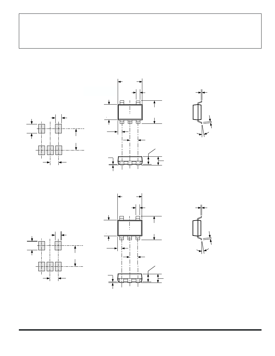
Dimensions in Inches
(for reference only)
Dimensions in Millimeters
(controlling dimensions)
0.018
0.012
Dwg. MA-010-15 in
1
3
0.0059
0.00
0.0079
0.0059
0.122
0.079
0.083
0.073
0.118
0.106
0.037
BSC
0.022
REF
4
0
°
TO
8
°
0.0098
MIN
0.043
0.035
0.049
0.035
2
5
Dwg. MA-011-5 mm
1
2
0.70
1.00
2.40
0.95
4
3
5
Dwg. MA-011-5 in
1
2
0.028
0.039
0.095
0.037
4
3
5
NOTES:
1. Tolerances on package height and width represent allowable mold offsets.
Dimensions given are measured at the widest point (parting line).
2. Exact body and lead configuration at vendor’s option within limits shown.
3. Height does not include mold gate flash.
4. Where no tolerance is specified, dimension is nominal.
Dwg. MA-010-15 mm
1
3
0.15
0.00
0.20
0.15
3.10
2.90
2.10
1.85
3.00
2.70
0.95
BSC
0.55
REF
0.45
0.30
4
0
°
TO
8
°
0.25
MIN
1.10
0.90
1.25
0.90
2
5

8205
LOW-DROPOUT
REGULATORS
115 Northeast Cutoff, Box 15036
Worcester, Massachusetts 01615-0036 (508) 853-5000
The products described here are manufactured under one or more
U.S. patents or U.S. patents pending.
Allegro MicroSystems, Inc. reserves the right to make, from time to
time, such departures from the detail specifications as may be required
to permit improvements in the performance, reliability, or
manufacturability of its products. Before placing an order, the user is
cautioned to verify that the information being relied upon is current.
Allegro products are not authorized for use as critical components
in life-support devices or systems without express written approval.
The information included herein is believed to be accurate and
reliable. However, Allegro MicroSystems, Inc. assumes no responsi-
bility for its use; nor for any infringement of patents or other rights of
third parties which may result from its use.
Wyszukiwarka
Podobne podstrony:
8205
8205
8205
8205
8205
8205
8205
8205
8205
8205
8205
więcej podobnych podstron