0.079 (2.0)
0.037 (0.95)
0.035 (0.9)
0.031 (0.8)
0.037 (0.9
Maximum Ratings and Thermal Characteristics
(T
A
= 25°C unless otherwise noted)
Parameter
Symbol
Value
Unit
Collector-Emitter Voltage
(base shorted)
BC817
V
CES
50
V
BC818
30
Collector-Emitter Voltage
(base open)
BC817
V
CEO
45
V
BC818
25
Emitter-Base Voltage
V
EBO
5
V
Collector Current
I
C
800
mA
Peak Collector Current
I
CM
1000
mA
Peak Base Current
I
BM
200
mA
Peak Emitter Current
–I
EM
1000
mA
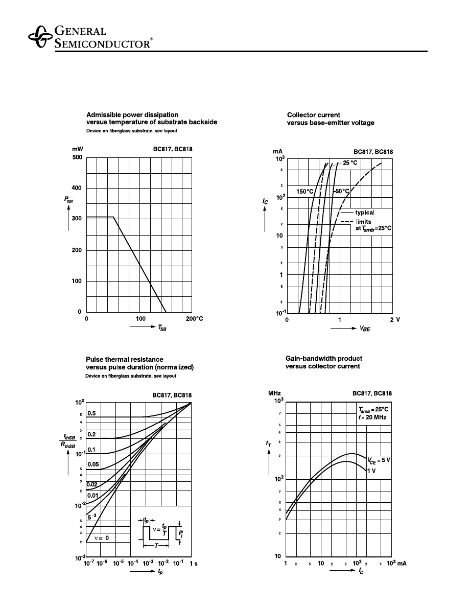
Power Dissipation at T
SB
= 50 ˚C
P
tot
310
(1)
mW
Thermal Resistance Junction to Ambiant Air
R
θ
JA
450
(1)
°C/W
Thermal Resistance Junction to Substrate Backside
R
θ
SB
320
(1)
°C/W
Junction Temperature
T
j
150
°C
Storage Temperature Range
T
S
–65 to +150
°C
Note: (1) Device on fiberglass substrate, see layout on third page.
BC817, BC818
Small Signal Transistors (NPN)
5/22/00
Dimensions in inches and (millimeters)
.016 (0.4)
.056 (
1
.43
)
.037(0.95) .037(0.95)
ma
x
. .004
(
0.1
)
.122 (3.1)
.016 (0.4)
.016 (0.4)
1
2
3
Top View
.102 (2.6)
.007 (
0
.17
5)
.0
45 (
1
.15)
.110 (2.8)
.052 (
1
.33
)
.005
(
0
.1
25)
.094 (2.4)
.0
37 (
0
.95)
Features
• NPN Silicon Epitaxial Planar Transistors for
switching, AF driver and amplifier applications.
• Especially suited for automatic insertion in thick
and thin-film circuits.
• These transistors are subdivided into three groups
-16, -25, and -40 according to their current gain.
• As complementary types, the PNP transistors
BC807 and BC808 are recommended.
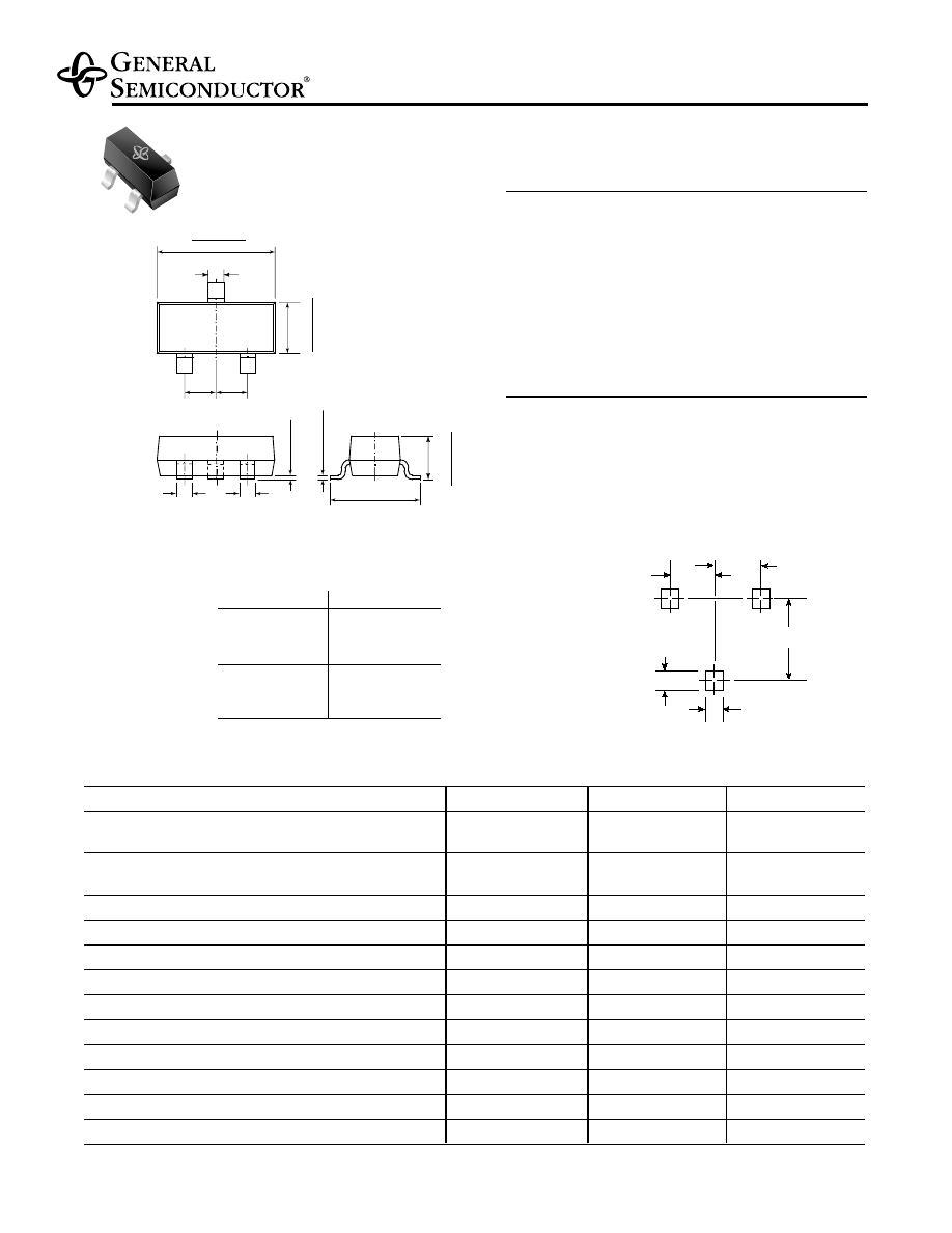
Mechanical Data
Case: SOT-23 Plastic Package
Weight: approx. 0.008g
Packaging Codes/Options:
E8/10K per 13” reel (8mm tape), 30K/box
E9/3K per 7” reel (8mm tape), 30K/box
TO-236AB (SOT-23)
Dimensions in inches and (millimeters)
Mounting Pad Layout
Type
Marking
BC817-16
6A
-25
6B
-40
6C
BC818-16
6E
-25
6F
-40
6G
Pin Configuration
1 = Base
2 = Emitter
3 = Collector
Electrical Characteristics
(T
J
= 25°C unless otherwise noted)
Parameter
Symbol
Test Condition
Min
Typ
Max
Unit
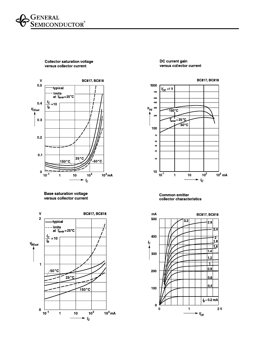
DC Current Gain
Current Gain Group-16
h
FE
V
CE
= 1V, I
C
= 100mA
100
—
250
—
-25
160
—
400
—
-40
250
—
600
—
h
FE
V
CE
= 1V, I
C
= 500mA
40
—
—
—
Collector Saturation Voltage
V
CEsat
I
C
= 500mA, I
B
= 50mA
—
—
0.7
V
Base Saturation Voltage
V
BEsat
I
C
= 500mA, I
B
= 50mA
—
—
1.3
V
Base-Emitter Voltage
V
BEon
V
CE
= 1V, I
C
= 500mA
—
—
1.2
V
Collector-Emitter Cutoff Current
BC817
I
CES
V
CE
= 45V
—
—
100
nA
BC818
V
CE
= 25V
—
—
100
nA
V
CE
= 25 V, T
j
= 150˚C
—
—
5
µ
A
Emitter-Base Cutoff Current
I
EBO
V
EB
= 4V
—
—
100
nA
Gain-Bandwidth Product
f
T
V
CE
= 5V, I
C
= 10mA
—
100
—
MHz
f = 50MHz
Collector-Base Capacitance
C
CBO
V
CB
= 10V, f = 1MHz
—
12
—
pF
Note:
(1) Device on fiberglass substrate, see layout on next page
0.59 (15)
0.2 (5)
0.03 (0.8)
0.30 (7.5)
0.12 (3)
.04 (1)
0.06 (1.5)
0.20 (5.1)
.08 (2)
.08 (2)
.04 (1)
0.47 (12)
Dimensions in inches (millimeters)
Layout for R
θ
JA
test
Thickness: Fiberglass 0.059 in. (1.5 mm)
Copper leads 0.012 in. (0.3 mm)
BC817, BC818
Small Signal Transistors (NPN)
BC817, BC818
Small Signal Transistors (NPN)
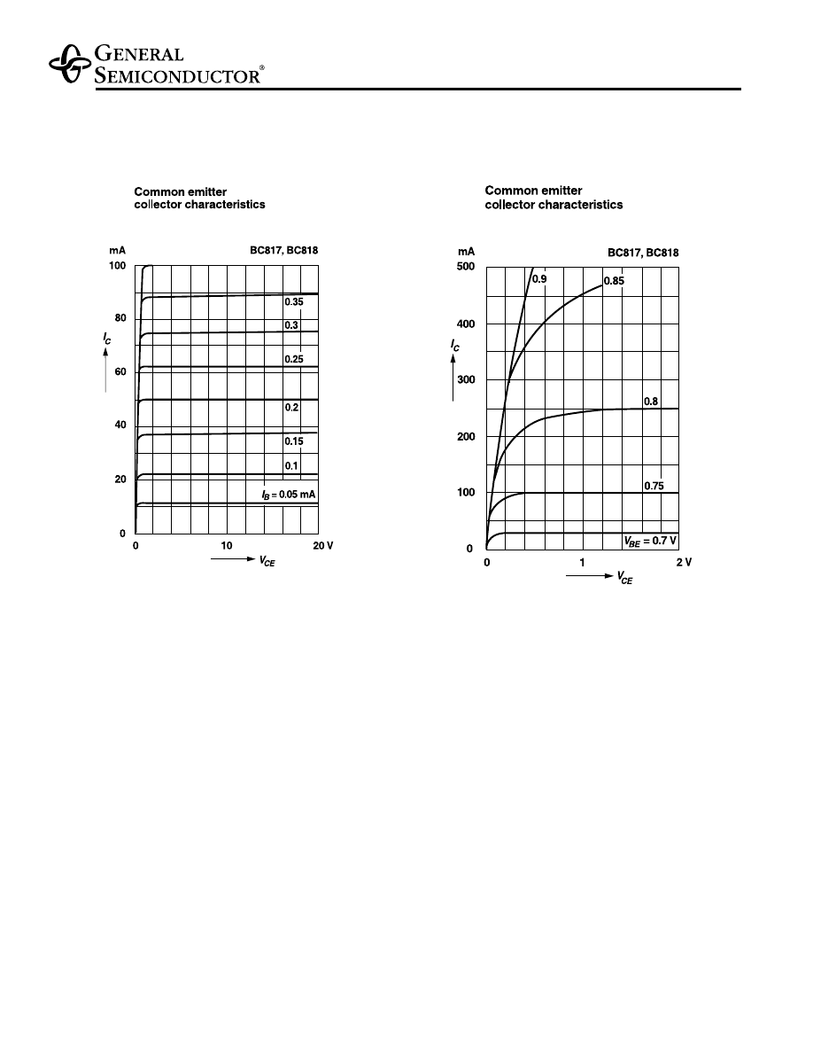
Ratings and
Characteristic Curves
(T
A
= 25°C unless otherwise noted)
BC817, BC818
Small Signal Transistors (NPN)
Ratings and
Characteristic Curves
(T
A
= 25°C unless otherwise noted)
BC817, BC818
Small Signal Transistors (NPN)
Ratings and
Characteristic Curves
(T
A
= 25°C unless otherwise noted)
Wyszukiwarka
Podobne podstrony:
bc817
BC817 BC337
bc817
BC817, BC818 (General Semiconductor)
BC817, BC818 (Vishay)
BC817 (Diodes Incorporated)
BC817, BC818 (Fairchild Semiconductor)
BC817 (Philips)
BC817, BC818 (Siemens)
BC817 (KEC)
więcej podobnych podstron