DS11107 Rev. 9 - 2
1 of 3
BC817-16/-25/-40
BC817-16 / -25 / -40
NPN SURFACE MOUNT SMALL SIGNAL TRANSISTOR
Features
Maximum Ratings
@T
A
= 25°C unless otherwise specified
Notes:
1. Device mounted on Ceramic Substrate 0.7mm; 2.5cm
2
area.
2. Short duration pulse test used to minimize self-heating effect.
Characteristic
Symbol
Value
Unit
Collector-Emitter Voltage
V
CEO
45
V
Emitter-Base Voltage
V
EBO
5.0
V
Collector Current
I
C
800
mA
Peak Collector Current
I
CM
1000
mA
Peak Emitter Current
I
EM
1000
mA
Power Dissipation at T
SB
= 50°C (Note 1)
P
d
310
mW
Thermal Resistance, Junction to Substrate Backside (Note 1)
R
qSB
320
°C/W
Thermal Resistance, Junction to Ambient Air (Note 1)
R
qJA
403
°C/W
Operating and Storage Temperature Range
T
j
, T
STG
-65 to +150
°C
·
Ideally Suited for Automatic Insertion
·
Epitaxial Planar Die Construction
·
For Switching, AF Driver and Amplifier
Applications
·
Complementary PNP Types Available (BC807)
·
Case: SOT-23, Molded Plastic
·
Case material - UL Flammability Rating
Classification 94V-0
·
Moisture sensitivity: Level 1 per J-STD-020A
·
Terminals: Solderable per MIL-STD-202, Method
208
·
Pin Connections: See Diagram
·
Marking (See Page 3): BC817-16 6A, K6A
BC817-25 6B, K6B
BC817-40 6C, K6C
·
Ordering & Date Code Information: See Page 3
·
Approx. Weight: 0.008 grams
Mechanical Data
Electrical Characteristics
@T
A
= 25°C unless otherwise specified
Characteristic (Note 2)
Symbol
Min
Max
Unit
Test Condition
DC Current Gain
Current Gain Group -16
-25
-40
Current Gain Group -16
-25
-40
h
FE
100
160
250
60
100
170
250
400
600
—
—
—
—
V
CE
= 1.0V, I
C
= 100mA
V
CE
= 1.0V, I
C
= 300mA
Collector-Emitter Saturation Voltage
V
CE(SAT)
—
0.7
V
I
C
= 500mA, I
B
= 50mA
Base-Emitter Voltage
V
BE
—
1.2
V
V
CE
= 1.0V, I
C
= 300mA
Collector-Emitter Cutoff Current
I
CES
—
100
5.0
nA
µA
V
CE
= 45V
V
CE
= 25V, T
j
= 150°C
Emitter-Base Cutoff Current
I
EBO
—
100
nA
V
EB
= 4.0V
Gain Bandwidth Product
f
T
100
—
MHz
V
CE
= 5.0V, I
C
= 10mA,
f = 50MHz
Collector-Base Capacitance
C
CBO
—
12
pF
V
CB
= 10V, f = 1.0MHz
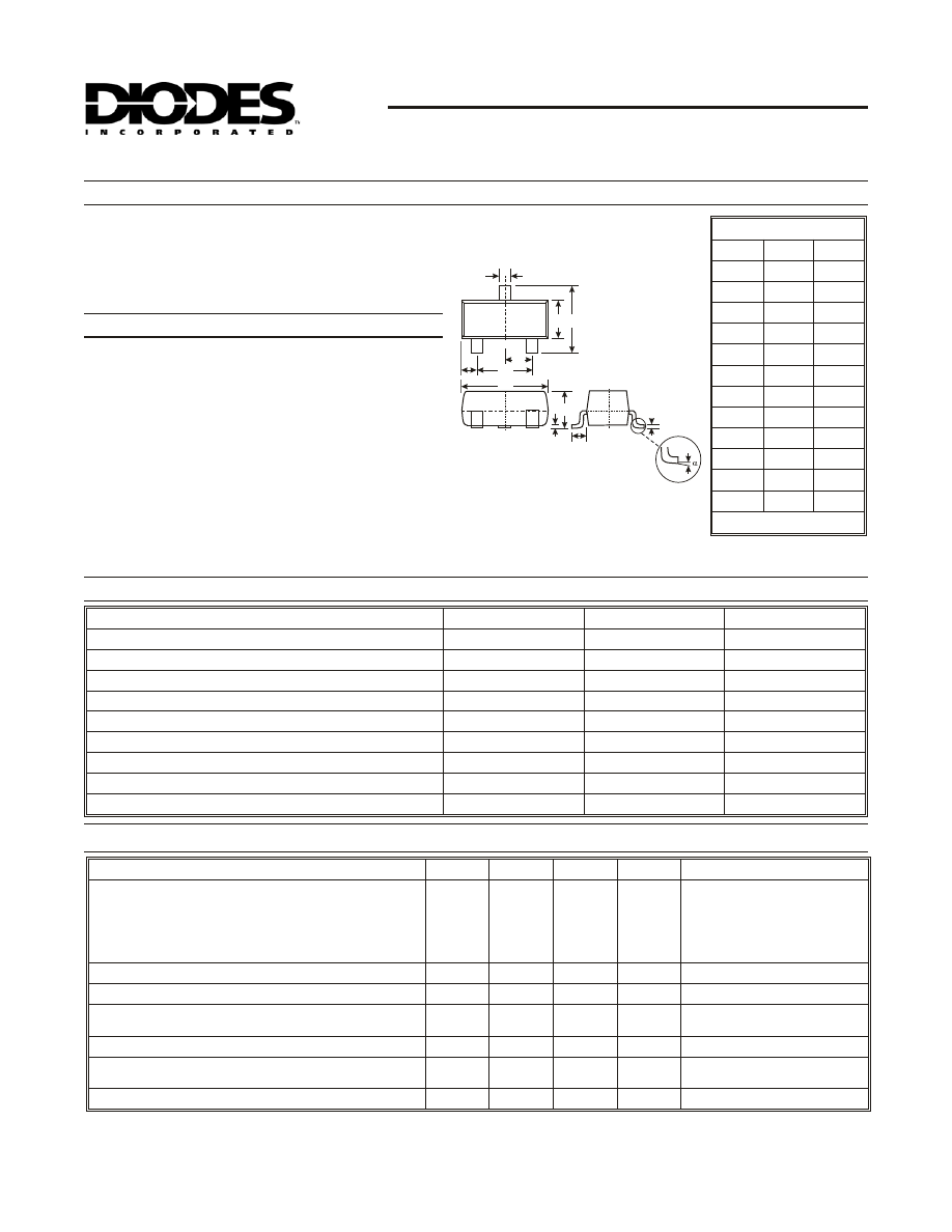
SOT-23
Dim
Min
Max
A
0.37
0.51
B
1.20
1.40
C
2.30
2.50
D
0.89
1.03
E
0.45
0.60
G
1.78
2.05
H
2.80
3.00
J
0.013
0.10
K
0.903
1.10
L
0.45
0.61
M
0.85
0.80
a
0
°
8
°
All Dimensions in mm
A
E
J
L
TOP VIEW
M
B
C
H
G
D
K
C
B
E

DS11107 Rev. 9 - 2
2 of 3
BC817-16/-25/-40
10
100
1000
1
10
100
1000
f
,
GAIN
BANDWIDTH
PRODUCT
(MHz)
T
I , COLLECTOR CURRENT (mA)
C
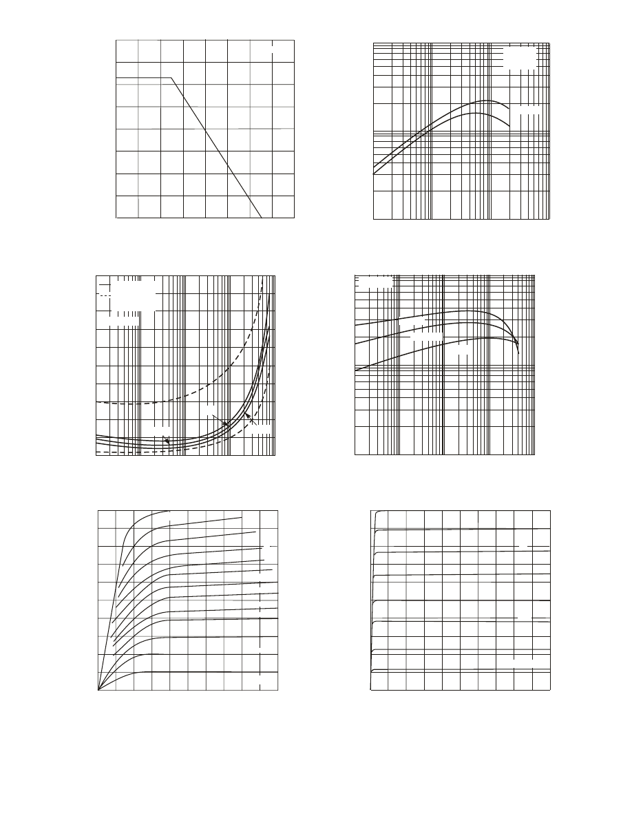
Fig. 2, Gain-Bandwidth Product vs Collector Current
T = 25
°C
A
f = 20MHz
V
= 5V
CE
1V
0
0.1
0.2
0.3
0.4
0.5
1
10
V
,
COLLECT
O
R
S
A
T
URA
T
ION
VOL
T
AGE
(V)
CE(SA
T
)
I , COLLECTOR CURRENT (mA)
C
Fig. 3, Collector Sat. Voltage vs Collector Current
typical
limits
at T = 25
°C
A
I / I = 10
C
B
150
°C
25
°C
-50
°C
100
1000
0.1
10
100
1000
1
10
h
,
DC
CURRENT
G
AIN
FE
I , COLLECTOR CURRENT (mA)
C
Fig. 4, DC Current Gain vs Collector Current
V
= 1V
CE
150
°C
T = 25
°C
A
-50
°C
100
1000
0.1
0
100
200
300
400
500
0
1
2
I
,
COLLECT
OR
CURRENT
(mA)
C
V
, COLLECTOR-EMITTER VOLTAGE (V)
CE
Fig. 5, Typical Emitter-Collector Characteristics
3.2
2.8
2
1.4
1.2
I = 0.2mA
B
0.8
0.6
0.4
1.6
2.4
1.8
0
20
40
60
80
100
0
10
20
I
,
COLLECT
O
R
CURRENT
(mA)
C
V
, COLLECTOR-EMITTER VOLTAGE (V)
CE
Fig. 6, Typical Emitter-Collector Characteristics
I = 0.05mA
B
0.1
0.15
0.2
0.25
0.3
0.35
0
100
200
300
400
0
100
200
P
,
POWER
D
ISSIP
A
TION
(mW)
d
T
, SUBSTRATE TEMPERATURE (
°C)
SB
Fig. 1, Power Derating Curve
See Note 1

DS11107 Rev. 9 - 2
3 of 3
BC817-16/-25/-40
Month
Jan
Feb
March
Apr
May
Jun
Jul
Aug
Sep
Oct
Nov
Dec
Code
1
2
3
4
5
6
7
8
9
O
N
D
Year
1998
1999
2000
2001
2002
2003
2004
Code
J
K
L
M
N
P
R
Date Code Key
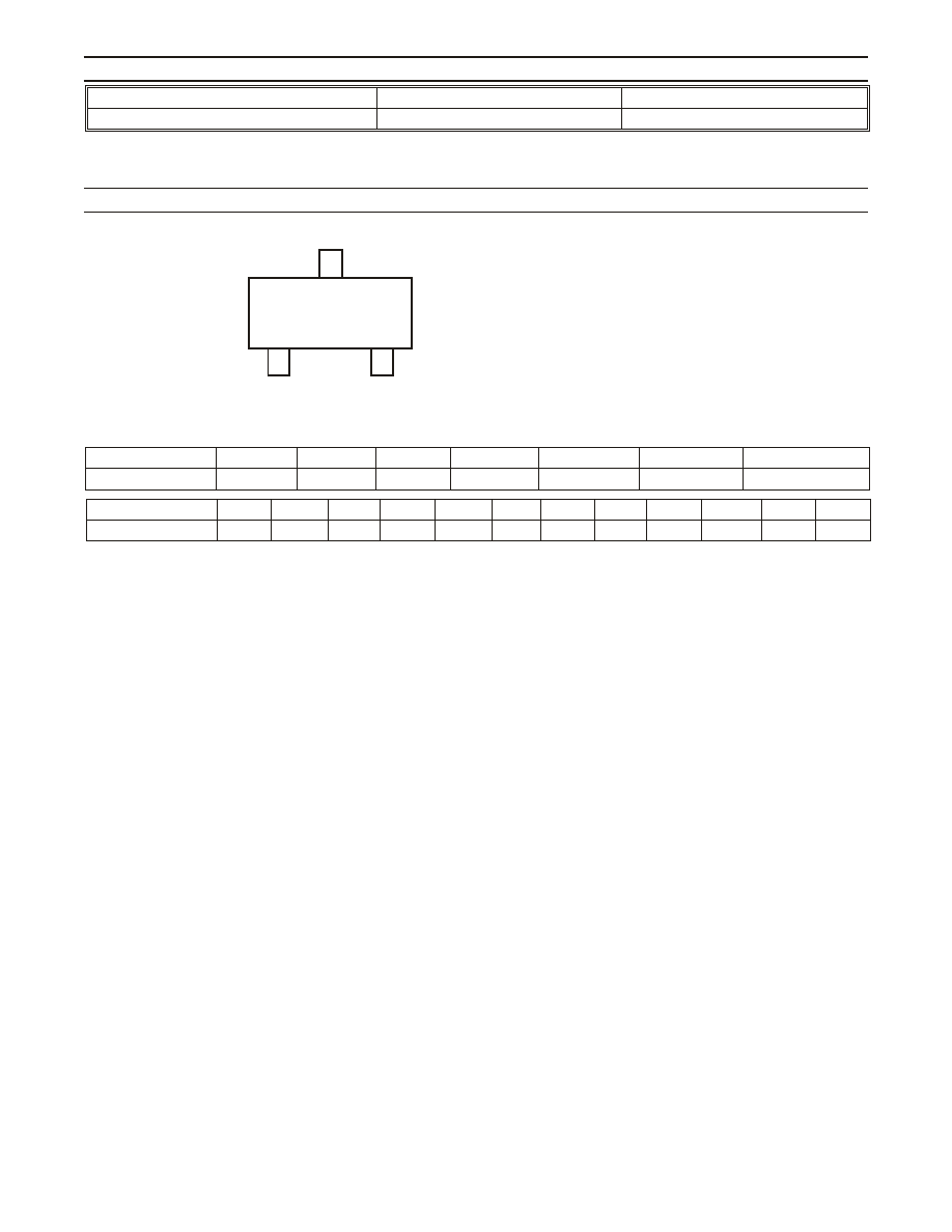
XXX = Product Type Marking Code (See Page 1), e.g. K6A = BC817-16
YM = Date Code Marking
Y = Year ex: N = 2002
M = Month ex: 9 = September
XXX
YM
Marking Information
Notes:
3. For Packaging Details, go to our website at http://www.diodes.com/datasheets/ap02007.pdf.
* xx = gain group, e.g. BC817-16-7.
Device*
Packaging
Shipping
BC817-xx-7
SOT-23
3000/Tape & Reel
Ordering Information
(Note 3)
Wyszukiwarka
Podobne podstrony:
BC807 (Diodes Incorporated)
Mars Incorporated
baker Is Head Movement Still Needed for Noun Incorporation
jagi.project.incorp, II rok II semestr, BWC, Kultura, kulturoznawstwo, Fw Fw Fw Kurwoznawstwo cz
bc817
A ZVS PWM Inverter With Active Voltage Clamping Using the Reverse Recovery Energy of the Diodes
BC817 BC337
Genotoxicidad inducida por plomo en personas laboralmente ex, UVM, encuentro de investigacion del si
3 INTRO TO DIODES
jagi.project.incorp., Muzealnictwo - ćwiczenia
Intraindividual stability in the organization and patterning of behavior Incorporating psychological
Light Emitting Diodes
Mars Incorporated
baker Is Head Movement Still Needed for Noun Incorporation
bc817
Light quality impovement for white electroluminescent diodes
The incorporation of carboxylate groups into temperature responsive poly(N isopropylacrylamide) base
więcej podobnych podstron