1
®
FN3082.4
ICL7106, ICL7107, ICL7107S
3
1
/
2
Digit, LCD/LED Display, A/D
Converters
The Intersil ICL7106 and ICL7107 are high performance, low
power, 3
1
/
2
digit A/D converters. Included are seven
segment decoders, display drivers, a reference, and a clock.
The ICL7106 is designed to interface with a liquid crystal
display (LCD) and includes a multiplexed backplane drive;
the ICL7107 will directly drive an instrument size light
emitting diode (LED) display.
The ICL7106 and ICL7107 bring together a combination of
high accuracy, versatility, and true economy. It features auto-
zero to less than 10
µ
V, zero drift of less than 1
µ
V/
o
C, input
bias current of 10pA (Max), and rollover error of less than
one count. True differential inputs and reference are useful in
all systems, but give the designer an uncommon advantage
when measuring load cells, strain gauges and other bridge
type transducers. Finally, the true economy of single power
supply operation (ICL7106), enables a high performance
panel meter to be built with the addition of only 10 passive
components and a display.
Features
• Guaranteed Zero Reading for 0V Input on All Scales
• True Polarity at Zero for Precise Null Detection
• 1pA Typical Input Current
• True Differential Input and Reference, Direct Display Drive
- LCD ICL7106, LED lCL7107
• Low Noise - Less Than 15
µ
V
P-P
• On Chip Clock and Reference
• Low Power Dissipation - Typically Less Than 10mW
• No Additional Active Circuits Required
• Enhanced Display Stability
Ordering Information
PART NO.
TEMP.
RANGE (
o
C)
PACKAGE
PKG. NO.
ICL7106CPL
0 to 70
40 Ld PDIP
E40.6
ICL7106CM44
0 to 70
44 Ld MQFP
Q44.10x10
ICL7107CPL
0 to 70
40 Ld PDIP
E40.6
ICL7107RCPL
0 to 70
40 Ld PDIP (Note)
E40.6
ICL7107SCPL
0 to 70
40 Ld PDIP (Note)
E40.6
ICL7107CM44
0 to 70
44 Ld MQFP
Q44.10x10
NOTE: “R” indicates device with reversed leads for mounting to PC
board underside. “S” indicates enhanced stability.
Data Sheet
August 2002
CAUTION: These devices are sensitive to electrostatic discharge; follow proper IC Handling Procedures.
1-888-INTERSIL or 321-724-7143
|
Intersil (and design) is a registered trademark of Intersil Americas Inc.
Copyright © Intersil Americas Inc. 2002. All Rights Reserved
2
Pinouts
ICL7106, ICL7107 (PDIP)
TOP VIEW
ICL7107R (PDIP)
TOP VIEW
ICL7106, ICL7107 (MQFP)
TOP VIEW
13
1
2
3
4
5
6
7
8
9
10
11
12
14
15
16
17
18
19
20
V+
D1
C1
B1
A1
F1
G1
E1
D2
C2
B2
A2
F2
E2
D3
B3
F3
E3
(1000) AB4
POL
28
40
39
38
37
36
35
34
33
32
31
30
29
27
26
25
24
23
22
21
OSC 1
OSC 2
OSC 3
TEST
REF HI
REF LO
C
REF
+
C
REF
-
COMMON
IN HI
IN LO
A-Z
BUFF
INT
V-
G2 (10’s)
C3
A3
G3
BP/GND
(1’s)
(10’s)
(100’s)
(MINUS)
(100’s)
OSC 2
NC
OSC 3
TEST
NC
NC
1
2
3
4
5
6
7
8
9
10
11
12 13 14 15 16 17
OSC 1
V+
D1
C1
B1
A1 F1 G1 E1 D2 C2
28
27
26
25
24
23
22
21
20
19
18
B2 A2 F2 E2 D3
B3
F3
E3
AB4
POL
BP/GND
39 38 37 36 35 34
33
32
31
30
29
44 43 42 41 40
IN H
I
IN L
O
A-
Z
BUFF
INT
V-
NC
G2
C3
A3
G3
RE
F
HI
RE
F
LO
C
RE
F
+
C
RE
F
-
CO
MMON
ICL7106, ICL7107, ICL7107S
3
Absolute Maximum Ratings
Thermal Information
Supply Voltage
ICL7106, V+ to V-. . . . . . . . . . . . . . . . . . . . . . . . . . . . . . . . . . .15V
ICL7107, V+ to GND . . . . . . . . . . . . . . . . . . . . . . . . . . . . . . . . .6V
ICL7107, V- to GND . . . . . . . . . . . . . . . . . . . . . . . . . . . . . . . . . -9V
Analog Input Voltage (Either Input) (Note 1) . . . . . . . . . . . . V+ to V-
Reference Input Voltage (Either Input). . . . . . . . . . . . . . . . . V+ to V-
Clock Input
ICL7106 . . . . . . . . . . . . . . . . . . . . . . . . . . . . . . . . . . . TEST to V+
ICL7107 . . . . . . . . . . . . . . . . . . . . . . . . . . . . . . . . . . . . GND to V+
Operating Conditions
Temperature Range . . . . . . . . . . . . . . . . . . . . . . . . . . . . 0
o
C to 70
o
C
Thermal Resistance (Typical, Note 2)
θ
JA
(
o
C/W)
PDIP Package . . . . . . . . . . . . . . . . . . . . . . . . . . . . .
50
MQFP Package . . . . . . . . . . . . . . . . . . . . . . . . . . . .
75
Maximum Junction Temperature . . . . . . . . . . . . . . . . . . . . . . .150
o
C
Maximum Storage Temperature Range . . . . . . . . . . -65
o
C to 150
o
C
Maximum Lead Temperature (Soldering 10s) . . . . . . . . . . . . .300
o
C
(MQFP - Lead Tips Only)
CAUTION: Stresses above those listed in “Absolute Maximum Ratings” may cause permanent damage to the device. This is a stress only rating and operation of the
device at these or any other conditions above those indicated in the operational sections of this specification is not implied.
NOTES:
1. Input voltages may exceed the supply voltages provided the input current is limited to
±
100
µ
A.
2.
θ
JA
is measured with the component mounted on a low effective thermal conductivity test board in free air. See Tech Brief TB379 for details.
Electrical Specifications
(Note 3)
PARAMETER
TEST CONDITIONS
MIN
TYP
MAX
UNIT
SYSTEM PERFORMANCE
Zero Input Reading
V
IN
= 0.0V, Full Scale = 200mV
-000.0
±
000.0
+000.0
Digital
Reading
Stability (Last Digit) (ICL7106S, ICL7107S
Only)
Fixed Input Voltage (Note 6)
-000.0
±
000.0
+000.0
Digital
Reading
Ratiometric Reading
V
lN
= V
REF
, V
REF
= 100mV
999
999/10
00
1000
Digital
Reading
Rollover Error
-V
IN
= +V
lN
≅
200mV
Difference in Reading for Equal Positive and Negative
Inputs Near Full Scale
-
±
0.2
±
1
Counts
Linearity
Full Scale = 200mV or Full Scale = 2V Maximum
Deviation from Best Straight Line Fit (Note 5)
-
±
0.2
±
1
Counts
Common Mode Rejection Ratio
V
CM
= 1V, V
IN
= 0V, Full Scale = 200mV (Note 5)
-
50
-
µ
V/V
Noise
V
IN
= 0V, Full Scale = 200mV
(Peak-To-Peak Value Not Exceeded 95% of Time)
-
15
-
µ
V
Leakage Current Input
V
lN
= 0 (Note 5)
-
1
10
pA
Zero Reading Drift
V
lN
= 0, 0
o
C To 70
o
C (Note 5)
-
0.2
1
µ
V/
o
C
Scale Factor Temperature Coefficient
V
IN
= 199mV, 0
o
C To 70
o
C
,
(Ext. Ref. 0ppm/×
o
C) (Note 5)
-
1
5
ppm/
o
C
End Power Supply Character V+ Supply
Current
V
IN
= 0 (Does Not Include LED Current for ICL7107)
-
1.0
1.8
mA
End Power Supply Character V- Supply Current ICL7107 Only
-
0.6
1.8
mA
COMMON Pin Analog Common Voltage
25k
Ω
Between Common and
Positive Supply (With Respect to + Supply)
2.4
3.0
3.2
V
Temperature Coefficient of Analog Common
25k
Ω
Between Common and
Positive Supply (With Respect to + Supply)
-
80
-
ppm/
o
C
DISPLAY DRIVER ICL7106 ONLY
Peak-To-Peak Segment Drive Voltage
Peak-To-Peak Backplane Drive Voltage
V+ = to V- = 9V (Note 4)
4
5.5
6
V
ICL7106, ICL7107, ICL7107S
4
DISPLAY DRIVER ICL7107 ONLY
Segment Sinking Current
V+ = 5V, Segment Voltage = 3V
Except Pins 19 and 20
5
8
-
mA
Pin 19 Only
10
16
-
mA
Pin 20 Only
4
7
-
mA
NOTES:
3. Unless otherwise noted, specifications apply to both the ICL7106 and ICL7107 at T
A
= 25
o
C, f
CLOCK
= 48kHz. ICL7106 is tested in the circuit
of Figure 1. ICL7107 is tested in the circuit of Figure 2.
4. Back plane drive is in phase with segment drive for “off” segment, 180 degrees out of phase for “on” segment. Frequency is 20 times conversion
rate. Average DC component is less than 50mV.
5. Not tested, guaranteed by design.
6. Sample Tested.
Typical Applications and Test Circuits
FIGURE 1. ICL7106 TEST CIRCUIT AND TYPICAL APPLICATION WITH LCD DISPLAY COMPONENTS SELECTED FOR 200mV FULL
SCALE
FIGURE 2. ICL7107 TEST CIRCUIT AND TYPICAL APPLICATION WITH LED DISPLAY COMPONENTS SELECTED FOR 200mV FULL
SCALE
Electrical Specifications
(Note 3) (Continued)
PARAMETER
TEST CONDITIONS
MIN
TYP
MAX
UNIT
13
1
2
3
4
5
6
7
8
9
10
11
12
14
15
16
17
18
19
20
28
40
39
38
37
36
35
34
33
32
31
30
29
27
26
25
24
23
22
21
V+
D1
C1
B1
A1
F1
G1
E1
D2
C2
B2
A2
F2
E2
D3
B3
F3
E3
AB
4
PO
L
OSC 1
OSC 2
OSC 3
TES
T
RE
F
H
I
R
E
F LO
C
REF
+
C
RE
F
-
COM
IN HI
IN LO
A-Z
BUF
F
INT
V-
G2
C3
A3
G3
BP
DISPLAY
DISPLAY
C
1
C
2
C
3
C
4
R
3
R
1
R
4
C
5
+
-
IN
R
5
R
2
9V
ICL7106
C
1
= 0.1
µ
F
C
2
= 0.47
µ
F
C
3
= 0.22
µ
F
C
4
= 100pF
C
5
= 0.02
µ
F
R
1
= 24k
Ω
R
2
= 47k
Ω
R
3
= 100k
Ω
R
4
= 1k
Ω
R
5
= 1M
Ω
+
-
13
1
2
3
4
5
6
7
8
9
10
11
12
14
15
16
17
18
19
20
28
40
39
38
37
36
35
34
33
32
31
30
29
27
26
25
24
23
22
21
V+
D1
C1
B1
A1
F1
G1
E1
D2
C2
B2
A2
F2
E2
D3
B3
F3
E3
AB4
PO
L
OS
C
1
OS
C
2
OS
C
3
TE
ST
RE
F HI
REF LO
C
RE
F
+
C
REF
-
COM
IN
H
I
IN
L
O
A-
Z
BUFF
INT
V-
G2
C3
A3
G3
GND
DISPLAY
DISPLAY
C
1
C
2
C
3
C
4
R
3
R
1
R
4
C
5
+
-
IN
R
5
R
2
ICL7107
+5V
-5V
C
1
= 0.1
µ
F
C
2
= 0.47
µ
F
C
3
= 0.22
µ
F
C
4
= 100pF
C
5
= 0.02
µ
F
R
1
= 24k
Ω
R
2
= 47k
Ω
R
3
= 100k
Ω
R
4
= 1k
Ω
R
5
= 1M
Ω
ICL7106, ICL7107, ICL7107S
5
Typical Integrator Amplifier Output Waveform (INT Pin)
Design Information Summary Sheet
• OSCILLATOR FREQUENCY
f
OSC
= 0.45/RC
C
OSC
> 50pF; R
OSC
> 50k
Ω
f
OSC
(Typ) = 48kHz
• OSCILLATOR PERIOD
t
OSC
= RC/0.45
• INTEGRATION CLOCK FREQUENCY
f
CLOCK
= f
OSC
/4
• INTEGRATION PERIOD
t
INT
= 1000 x (4/f
OSC
)
• 60/50Hz REJECTION CRITERION
t
INT
/t
60Hz
or t
lNT
/t
60Hz
= Integer
• OPTIMUM INTEGRATION CURRENT
I
INT
= 4
µ
A
• FULL SCALE ANALOG INPUT VOLTAGE
V
lNFS
(Typ) = 200mV or 2V
• INTEGRATE RESISTOR
• INTEGRATE CAPACITOR
• INTEGRATOR OUTPUT VOLTAGE SWING
• V
INT
MAXIMUM SWING:
(V- + 0.5V) < V
INT
< (V+ - 0.5V), V
INT
(Typ) = 2V
• DISPLAY COUNT
• CONVERSION CYCLE
t
CYC
= t
CL0CK
x 4000
t
CYC
= t
OSC
x 16,000
when f
OSC
= 48kHz; t
CYC
= 333ms
• COMMON MODE INPUT VOLTAGE
(V- + 1V) < V
lN
< (V+ - 0.5V)
• AUTO-ZERO CAPACITOR
0.01
µ
F < C
AZ
< 1
µ
F
• REFERENCE CAPACITOR
0.1
µ
F < C
REF
< 1
µ
F
• V
COM
Biased between Vi and V-.
• V
COM
≅
V+ - 2.8V
Regulation lost when V+ to V- <
≅
6.8V
If V
COM
is externally pulled down to (V+ to V-)/2,
the V
COM
circuit will turn off.
• ICL7106 POWER SUPPLY: SINGLE 9V
V+ - V- = 9V
Digital supply is generated internally
V
GND
≅
V+ - 4.5V
• ICL7106 DISPLAY: LCD
Type: Direct drive with digital logic supply amplitude.
• ICL7107 POWER SUPPLY: DUAL
±
5.0V
V+ = +5V to GND
V- = -5V to GND
Digital Logic and LED driver supply V+ to GND
• ICL7107 DISPLAY: LED
Type: Non-Multiplexed Common Anode
R
INT
V
INFS
I
INT
-----------------
=
C
INT
t
INT
(
)
I
INT
(
)
V
INT
--------------------------------
=
V
INT
t
INT
(
)
I
INT
(
)
C
INT
--------------------------------
=
COUNT
1000
V
IN
V
REF
---------------
×
=
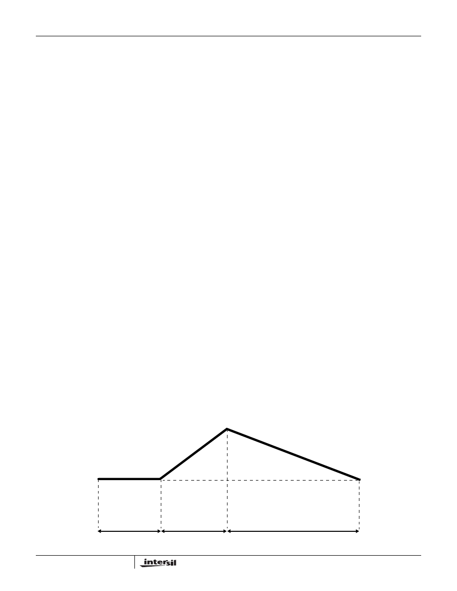
AUTO ZERO PHASE
(COUNTS)
2999 - 1000
SIGNAL INTEGRATE
PHASE FIXED
1000 COUNTS
DE-INTEGRATE PHASE
0 - 1999 COUNTS
TOTAL CONVERSION TIME = 4000 x t
CLOCK
= 16,000 x t
OSC
ICL7106, ICL7107, ICL7107S

6
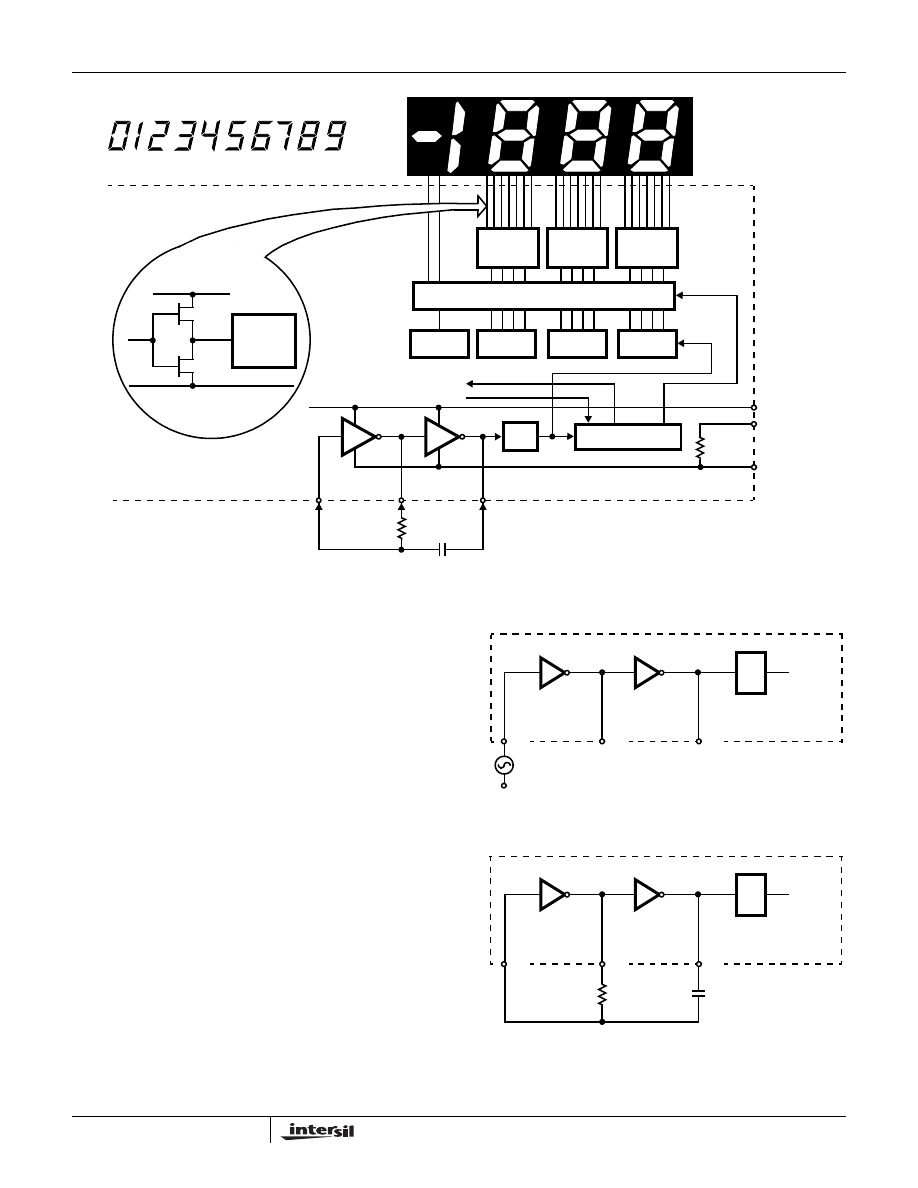
Detailed Description
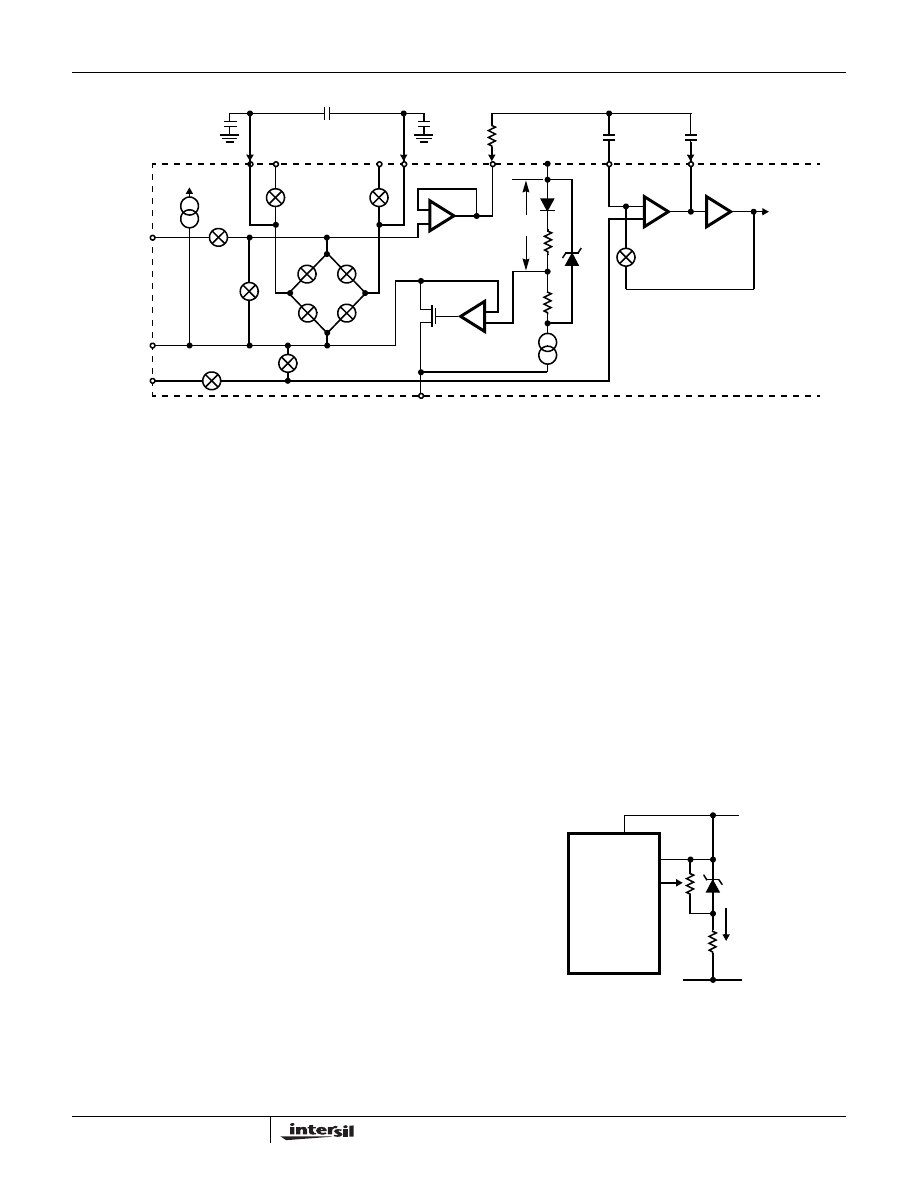
Analog Section
Figure 3 shows the Analog Section for the ICL7106 and
ICL7107. Each measurement cycle is divided into three
phases. They are (1) auto-zero (A-Z), (2) signal integrate
(INT) and (3) de-integrate (DE).
Auto-Zero Phase
During auto-zero three things happen. First, input high and low
are disconnected from the pins and internally shorted to analog
COMMON. Second, the reference capacitor is charged to the
reference voltage. Third, a feedback loop is closed around the
system to charge the auto-zero capacitor C
AZ
to compensate
for offset voltages in the buffer amplifier, integrator, and
comparator. Since the comparator is included in the loop, the A-
Z accuracy is limited only by the noise of the system. In any
case, the offset referred to the input is less than 10
µ
V.
Signal Integrate Phase
During signal integrate, the auto-zero loop is opened, the
internal short is removed, and the internal input high and low
are connected to the external pins. The converter then
integrates the differential voltage between IN HI and IN LO for a
fixed time. This differential voltage can be within a wide
common mode range: up to 1V from either supply. If, on the
other hand, the input signal has no return with respect to the
converter power supply, IN LO can be tied to analog COMMON
to establish the correct common mode voltage. At the end of
this phase, the polarity of the integrated signal is determined.
De-Integrate Phase
The final phase is de-integrate, or reference integrate. Input
low is internally connected to analog COMMON and input
high is connected across the previously charged reference
capacitor. Circuitry within the chip ensures that the capacitor
will be connected with the correct polarity to cause the
integrator output to return to zero. The time required for the
output to return to zero is proportional to the input signal.
Specifically the digital reading displayed is:
.
Differential Input
The input can accept differential voltages anywhere within the
common mode range of the input amplifier, or specifically from
0.5V below the positive supply to 1V above the negative
supply. In this range, the system has a CMRR of 86dB typical.
However, care must be exercised to assure the integrator
output does not saturate. A worst case condition would be a
large positive common mode voltage with a near full scale
negative differential input voltage. The negative input signal
drives the integrator positive when most of its swing has been
used up by the positive common mode voltage. For these
critical applications the integrator output swing can be
reduced to less than the recommended 2V full scale swing
with little loss of accuracy. The integrator output can swing to
within 0.3V of either supply without loss of linearity.
Differential Reference
The reference voltage can be generated anywhere within the
power supply voltage of the converter. The main source of
common mode error is a roll-over voltage caused by the
reference capacitor losing or gaining charge to stray capacity
on its nodes. If there is a large common mode voltage, the
reference capacitor can gain charge (increase voltage) when
called up to de-integrate a positive signal but lose charge
(decrease voltage) when called up to de-integrate a negative
input signal. This difference in reference for positive or negative
input voltage will give a roll-over error. However, by selecting
the reference capacitor such that it is large enough in
comparison to the stray capacitance, this error can be held to
less than 0.5 count worst case. (See Component Value
Selection.)
DISPLAY COUNT = 1000
V
IN
V
REF
---------------
ICL7106, ICL7107, ICL7107S
7
Analog COMMON
This pin is included primarily to set the common mode
voltage for battery operation (ICL7106) or for any system
where the input signals are floating with respect to the power
supply. The COMMON pin sets a voltage that is
approximately 2.8V more negative than the positive supply.
This is selected to give a minimum end-of-life battery voltage
of about 6V. However, analog COMMON has some of the
attributes of a reference voltage. When the total supply
voltage is large enough to cause the zener to regulate (>7V),
the COMMON voltage will have a low voltage coefficient
(0.001%/V), low output impedance (
≅
15
Ω
), and a
temperature coefficient typically less than 80ppm/×
o
C.
The limitations of the on chip reference should also be
recognized, however. With the ICL7107, the internal heating
which results from the LED drivers can cause some
degradation in performance. Due to their higher thermal
resistance, plastic parts are poorer in this respect than
ceramic. The combination of reference Temperature
Coefficient (TC), internal chip dissipation, and package
thermal resistance can increase noise near full scale from
25
µ
V to 80
µ
V
P-P
. Also the linearity in going from a high
dissipation count such as 1000 (20 segments on) to a low
dissipation count such as 1111(8 segments on) can suffer by a
count or more. Devices with a positive TC reference may
require several counts to pull out of an over-range condition.
This is because over-range is a low dissipation mode, with the
three least significant digits blanked. Similarly, units with a
negative TC may cycle between over-range and a non-over-
range count as the die alternately heats and cools. All these
problems are of course eliminated if an external reference is
used.
The ICL7106, with its negligible dissipation, suffers from
none of these problems. In either case, an external
reference can easily be added, as shown in Figure 4.
Analog COMMON is also used as the input low return during
auto-zero and de-integrate. If IN LO is different from analog
COMMON, a common mode voltage exists in the system
and is taken care of by the excellent CMRR of the converter.
However, in some applications IN LO will be set at a fixed
known voltage (power supply common for instance). In this
application, analog COMMON should be tied to the same
point, thus removing the common mode voltage from the
converter. The same holds true for the reference voltage. If
reference can be conveniently tied to analog COMMON, it
should be since this removes the common mode voltage
from the reference system.
Within the lC, analog COMMON is tied to an N-Channel FET
that can sink approximately 30mA of current to hold the
voltage 2.8V below the positive supply (when a load is trying
to pull the common line positive). However, there is only
10
µ
A of source current, so COMMON may easily be tied to a
more negative voltage thus overriding the internal reference.
FIGURE 3. ANALOG SECTION OF ICL7106 AND ICL7107
DE
-
DE+
C
INT
C
AZ
R
INT
BUFFER
A-Z
INT
-
+
A-Z
COMPARATOR
IN HI
COMMON
IN LO
31
32
30
DE-
DE+
INT
A-Z
34
C
REF
+
36
REF HI
C
REF
REF LO
35
A-Z
A-Z
33
C
REF
-
28
29
27
TO
DIGITAL
SECTION
A-Z AND DE
(±)
INTEGRATOR
INT
STRAY
STRAY
V+
10
µ
A
V-
N
INPUT
HIGH
2.8V
6.2V
V+
1
INPUT
LOW
-
+
-
+
-
+
FIGURE 4A.
ICL7106
V
REF LO
ICL7107
REF HI
V+
V-
6.8V
ZENER
I
Z
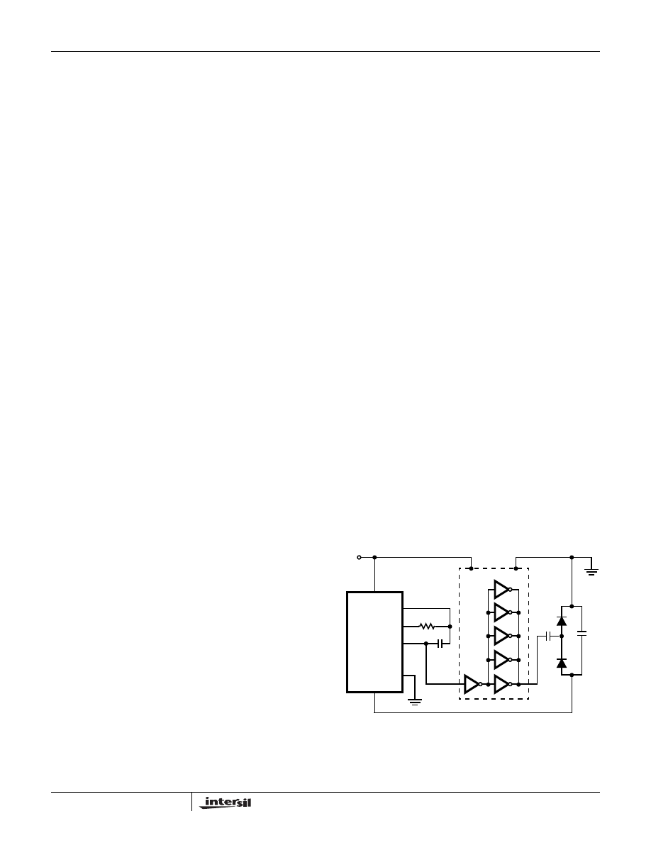
ICL7106, ICL7107, ICL7107S
8
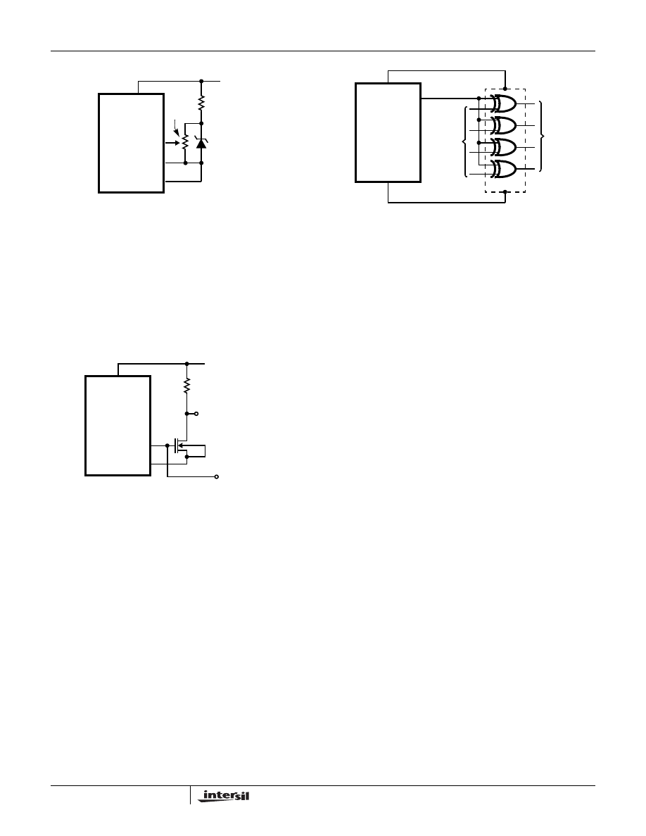
TEST
The TEST pin serves two functions. On the ICL7106 it is
coupled to the internally generated digital supply through a
500
Ω
resistor. Thus it can be used as the negative supply for
externally generated segment drivers such as decimal points
or any other presentation the user may want to include on
the LCD display. Figures 5 and 6 show such an application.
No more than a 1mA load should be applied.
The second function is a “lamp test”. When TEST is pulled
high (to V+) all segments will be turned on and the display
should read “1888”. The TEST pin will sink about 15mA
under these conditions.
CAUTION: In the lamp test mode, the segments have a constant DC
voltage (no square-wave). This may burn the LCD display if main-
tained for extended periods.
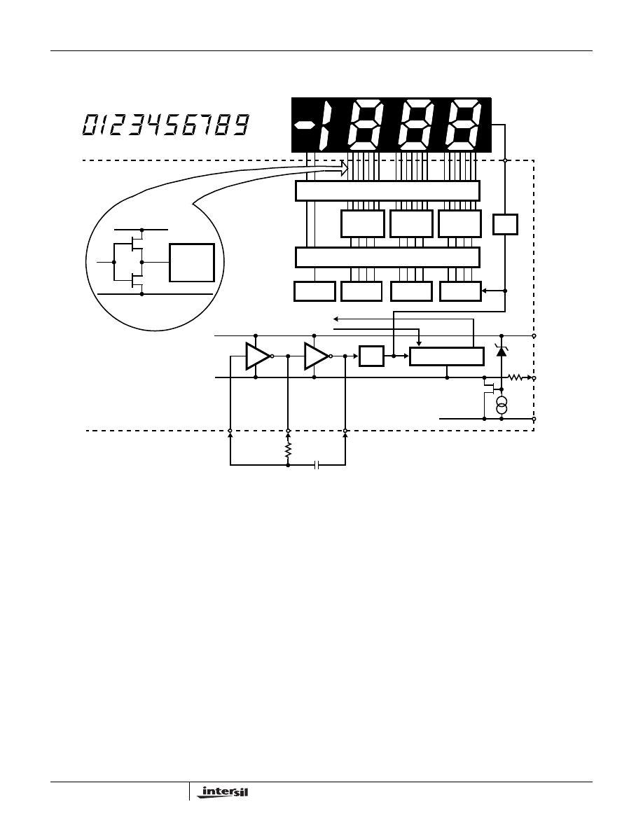
Digital Section
Figures 7 and 8 show the digital section for the ICL7106 and
ICL7107, respectively. In the ICL7106, an internal digital
ground is generated from a 6V Zener diode and a large
P-Channel source follower. This supply is made stiff to
absorb the relative large capacitive currents when the back
plane (BP) voltage is switched. The BP frequency is the
clock frequency divided by 800. For three readings/sec., this
is a 60Hz square wave with a nominal amplitude of 5V. The
segments are driven at the same frequency and amplitude
and are in phase with BP when OFF, but out of phase when
ON. In all cases negligible DC voltage exists across the
segments.
Figure 8 is the Digital Section of the ICL7107. It is identical to
the ICL7106 except that the regulated supply and back
plane drive have been eliminated and the segment drive has
been increased from 2mA to 8mA, typical for instrument size
common anode LED displays. Since the 1000 output (pin
19) must sink current from two LED segments, it has twice
the drive capability or 16mA.
In both devices, the polarity indication is “on” for negative
analog inputs. If IN LO and IN HI are reversed, this indication
can be reversed also, if desired.
FIGURE 4B.
FIGURE 4. USING AN EXTERNAL REFERENCE
ICL7106
V
REF HI
REF LO
COMMON
V+
ICL8069
1.2V
REFERENCE
6.8k
Ω
20k
Ω
ICL7107
ICL7106
V+
BP
TEST
21
37
TO LCD
BACKPLANE
TO LCD
DECIMAL
POINT
1M
Ω
FIGURE 5. SIMPLE INVERTER FOR FIXED DECIMAL POINT
ICL7106
V+
BP
TEST
DECIMAL
POINT
SELECT
CD4030
GND
V+
TO LCD
DECIMAL
POINTS
FIGURE 6. EXCLUSIVE ‘OR’ GATE FOR DECIMAL POINT DRIVE
ICL7106, ICL7107, ICL7107S
9
7
SEGMENT
DECODE
SEGMENT
OUTPUT
0.5mA
2mA
INTERNAL DIGITAL GROUND
TYPICAL SEGMENT OUTPUT
V+
LCD PHASE DRIVER
LATCH
7
SEGMENT
DECODE
÷
200
LOGIC CONTROL
INTERNAL
V
TH
= 1V
7
SEGMENT
DECODE
1000’s
100’s
10’s
1’s
TO SWITCH DRIVERS
FROM COMPARATOR OUTPUT
DIGITAL
GROUND
÷
4
CLOCK
40
39
38
OSC 1
OSC 2
OSC 3
BACKPLANE
21
V+
TEST
V-
500
Ω
37
26
6.2V
COUNTER
COUNTER
COUNTER
COUNTER
1
c
a
b
c
d
f
g
e
a
b
a
b
c
d
f
g
e
a
b
c
d
f
g
e
†
†
THREE INVERTERS
ONE INVERTER SHOWN FOR CLARITY
FIGURE 7. ICL7106 DIGITAL SECTION
ICL7106, ICL7107, ICL7107S
10
System Timing
Figure 9 shows the clocking arrangement used in the
ICL7106 and ICL7107. Two basic clocking arrangements
can be used:
1. Figure 9A. An external oscillator connected to pin 40.
2. Figure 9B. An R-C oscillator using all three pins.
The oscillator frequency is divided by four before it clocks
the decade counters. It is then further divided to form the
three convert-cycle phases. These are signal integrate
(1000 counts), reference de-integrate (0 to 2000 counts) and
auto-zero (1000 to 3000 counts). For signals less than full
scale, auto-zero gets the unused portion of reference
de-integrate. This makes a complete measure cycle of 4,000
counts (16,000 clock pulses) independent of input voltage.
For three readings/second, an oscillator frequency of 48kHz
would be used.
To achieve maximum rejection of 60Hz pickup, the signal
integrate cycle should be a multiple of 60Hz. Oscillator
frequencies of 240kHz, 120kHz, 80kHz, 60kHz, 48kHz,
40kHz, 33
1
/
3
kHz, etc. should be selected. For 50Hz
rejection, Oscillator frequencies of 200kHz, 100kHz,
66
2
/
3
kHz, 50kHz, 40kHz, etc. would be suitable. Note that
40kHz (2.5 readings/second) will reject both 50Hz and 60Hz
(also 400Hz and 440Hz).
7
SEGMENT
DECODE
TO
SEGMENT
0.5mA
8mA
DIGITAL GROUND
TYPICAL SEGMENT OUTPUT
V+
LATCH
7
SEGMENT
DECODE
LOGIC CONTROL
7
SEGMENT
DECODE
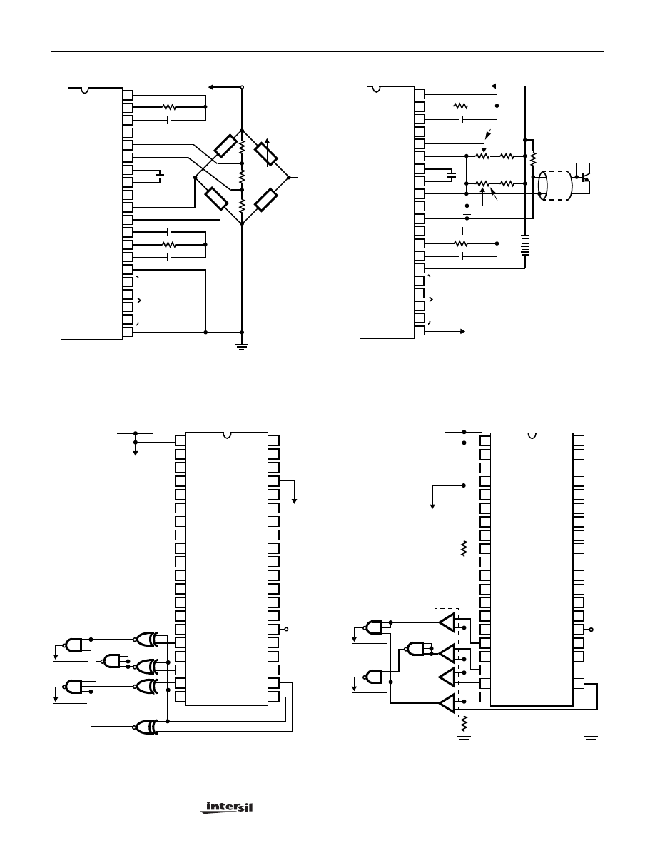
1000’s
100’s
10’s
1’s
TO SWITCH DRIVERS
FROM COMPARATOR OUTPUT
DIGITAL
GROUND
÷
4
CLOCK
40
39
38
OSC 1
OSC 2
OSC 3
V+
TEST
500
Ω
COUNTER
COUNTER
COUNTER
COUNTER
1
V+
37
27
c
a
b
c
d
f
g
e
a
b
a
b
c
d
f
g
e
a
b
c
d
f
g
e
†
†
THREE INVERTERS
ONE INVERTER SHOWN FOR CLARITY
FIGURE 8. ICL7107 DIGITAL SECTION
CLOCK
INTERNAL TO PART
40
39
38
GND ICL7107
÷
4
CLOCK
INTERNAL TO PART
40
39
38
÷
4
RC OSCILLATOR
R
C
TEST ICL7106
FIGURE 9B.
FIGURE 9. CLOCK CIRCUITS
FIGURE 9A.
ICL7106, ICL7107, ICL7107S
11
Component Value Selection
Integrating Resistor
Both the buffer amplifier and the integrator have a class A
output stage with 100
µ
A of quiescent current. They can
supply 4
µ
A of drive current with negligible nonlinearity. The
integrating resistor should be large enough to remain in this
very linear region over the input voltage range, but small
enough that undue leakage requirements are not placed on
the PC board. For 2V full scale, 470k
Ω
is near optimum and
similarly a 47k
Ω
for a 200mV scale.
Integrating Capacitor
The integrating capacitor should be selected to give the
maximum voltage swing that ensures tolerance buildup will
not saturate the integrator swing (approximately. 0.3V from
either supply). In the ICL7106 or the ICL7107, when the
analog COMMON is used as a reference, a nominal +2V full-
scale integrator swing is fine. For the ICL7107 with +5V
supplies and analog COMMON tied to supply ground, a
±
3.5V to +4V swing is nominal. For three readings/second
(48kHz clock) nominal values for C
lNT
are 0.22
µ
F and
0.10
µ
F, respectively. Of course, if different oscillator
frequencies are used, these values should be changed in
inverse proportion to maintain the same output swing.
An additional requirement of the integrating capacitor is that
it must have a low dielectric absorption to prevent roll-over
errors. While other types of capacitors are adequate for this
application, polypropylene capacitors give undetectable
errors at reasonable cost.
Auto-Zero Capacitor
The size of the auto-zero capacitor has some influence on
the noise of the system. For 200mV full scale where noise is
very important, a 0.47
µ
F capacitor is recommended. On the
2V scale, a 0.047
µ
F capacitor increases the speed of
recovery from overload and is adequate for noise on this
scale.
Reference Capacitor
A 0.1
µ
F capacitor gives good results in most applications.
However, where a large common mode voltage exists (i.e.,
the REF LO pin is not at analog COMMON) and a 200mV
scale is used, a larger value is required to prevent roll-over
error. Generally 1
µ
F will hold the roll-over error to 0.5 count
in this instance.
Oscillator Components
For all ranges of frequency a 100k
Ω
resistor is recommended
and the capacitor is selected from the equation:
Reference Voltage
The analog input required to generate full scale output (2000
counts) is: V
lN
= 2V
REF
. Thus, for the 200mV and 2V scale,
V
REF
should equal 100mV and 1V, respectively. However, in
many applications where the A/D is connected to a
transducer, there will exist a scale factor other than unity
between the input voltage and the digital reading. For
instance, in a weighing system, the designer might like to
have a full scale reading when the voltage from the
transducer is 0.662V. Instead of dividing the input down to
200mV, the designer should use the input voltage directly
and select V
REF
= 0.341V. Suitable values for integrating
resistor and capacitor would be 120k
Ω
and 0.22
µ
F. This
makes the system slightly quieter and also avoids a divider
network on the input. The ICL7107 with
±
5V supplies can
accept input signals up to
±
4V. Another advantage of this
system occurs when a digital reading of zero is desired for
V
IN
≠
0. Temperature and weighing systems with a variable
fare are examples. This offset reading can be conveniently
generated by connecting the voltage transducer between IN
HI and COMMON and the variable (or fixed) offset voltage
between COMMON and IN LO.
ICL7107 Power Supplies
The ICL7107 is designed to work from
±
5V supplies.
However, if a negative supply is not available, it can be
generated from the clock output with 2 diodes, 2 capacitors,
and an inexpensive lC. Figure 10 shows this application.
See ICL7660 data sheet for an alternative.
In fact, in selected applications no negative supply is
required. The conditions to use a single +5V supply are:
1. The input signal can be referenced to the center of the
common mode range of the converter.
2. The signal is less than
±
1.5V.
3. An external reference is used.
f
0.45
RC
----------- For 48kHz Clock (3 Readings/sec),
=
C
100pF.
=
ICL7107
V+
OSC 1
V-
OSC 2
OSC 3
GND
V+
V- = 3.3V
0.047
µ
F
10
µ
F
+
-
1N914
1N914
CD4009
FIGURE 10. GENERATING NEGATIVE SUPPLY FROM +5V
ICL7106, ICL7107, ICL7107S
12
Typical Applications
The ICL7106 and ICL7107 may be used in a wide variety of
configurations. The circuits which follow show some of the
possibilities, and serve to illustrate the exceptional versatility
of these A/D converters.
The following application notes contain very useful
information on understanding and applying this part and are
available from Intersil Corporation.
Application Notes
NOTE #
DESCRIPTION
AN016
“Selecting A/D Converters”
AN017
“The Integrating A/D Converter”
AN018
“Do’s and Don’ts of Applying A/D Converters”
AN023
“Low Cost Digital Panel Meter Designs”
AN032
“Understanding the Auto-Zero and Common Mode
Performance of the ICL7136/7/9 Family”
AN046
“Building a Battery-Operated Auto Ranging DVM with the
ICL7106”
AN052
“Tips for Using Single Chip 3
1
/
2
Digit A/D Converters”
AN9609 “Overcoming Common Mode Range Issues When Using
Intersil Integrating Converters”
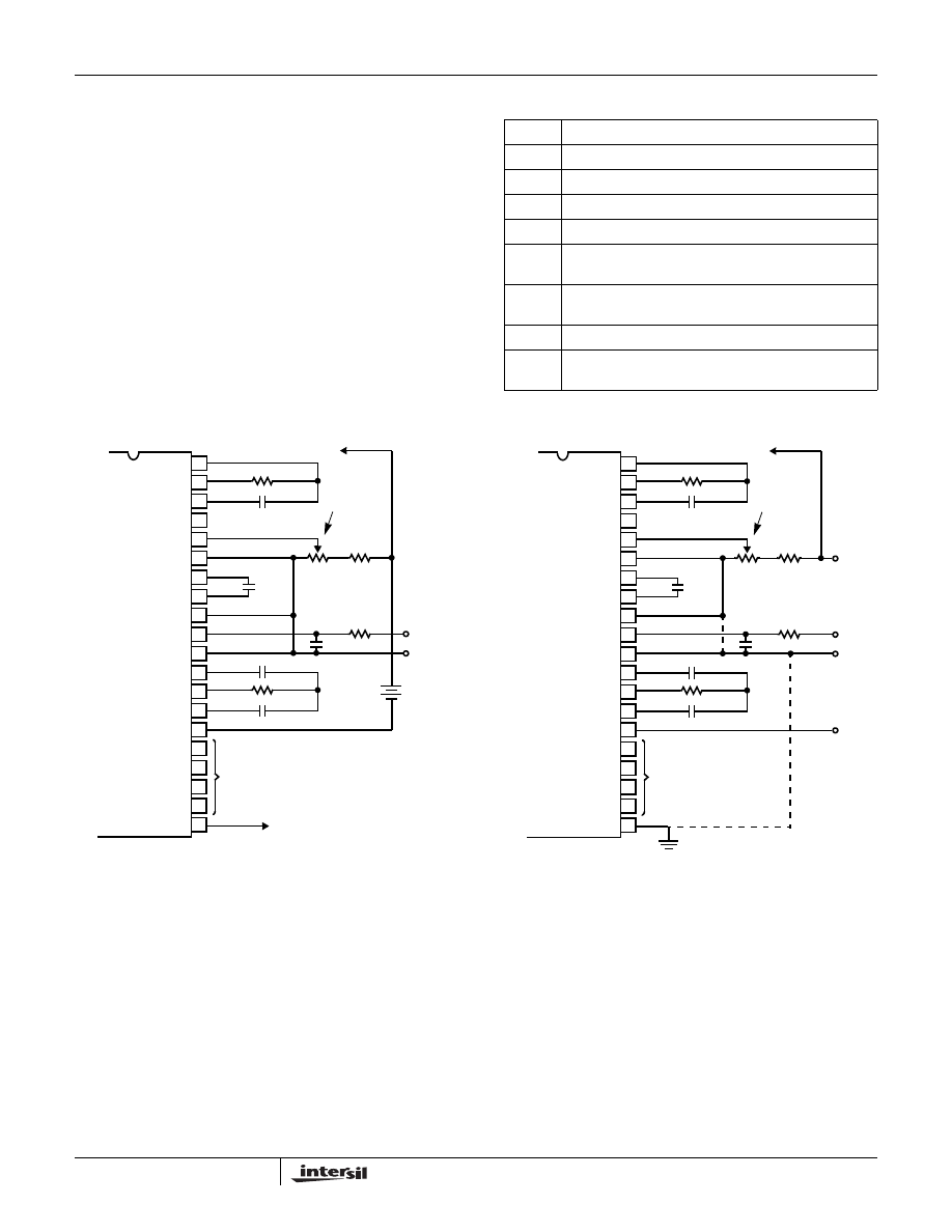
Typical Applications
FIGURE 11. ICL7106 USING THE INTERNAL REFERENCE
FIGURE 12. ICL7107 USING THE INTERNAL REFERENCE
28
40
39
38
37
36
35
34
33
32
31
30
29
27
26
25
24
23
22
21
OSC 1
OSC 2
OSC 3
TEST
REF HI
REF LO
C
REF
C
REF
COMMON
IN HI
IN LO
A-Z
BUFF
INT
V -
G2
C3
A3
G3
BP
100pF
TO PIN 1
SET V
REF
= 100mV
0.1
µ
F
0.01
µ
F
1M
Ω
100k
Ω
1k
Ω
22k
Ω
IN
+
-
9V
47k
Ω
0.22
µ
F
0.47
µ
F
TO BACKPLANE
TO DISPLAY
Values shown are for 200mV full scale, 3 readings/sec., floating
supply voltage (9V battery).
+
-
Values shown are for 200mV full scale, 3 readings/sec. IN LO may
be tied to either COMMON for inputs floating with respect to
supplies, or GND for single ended inputs. (See discussion under
Analog COMMON).
28
40
39
38
37
36
35
34
33
32
31
30
29
27
26
25
24
23
22
21
OSC 1
OSC 2
OSC 3
TEST
REF HI
REF LO
C
REF
C
REF
COMMON
IN HI
IN LO
A-Z
BUFF
INT
V -
G2
C3
A3
G3
GND
100pF
TO PIN 1
SET V
REF
= 100mV
0.1
µ
F
0.01
µ
F
1M
Ω
100k
Ω
1k
Ω
22k
Ω
IN
+
-
47k
Ω
0.22
µ
F
0.47
µ
F
TO DISPLAY
+5V
-5V
ICL7106, ICL7107, ICL7107S
13
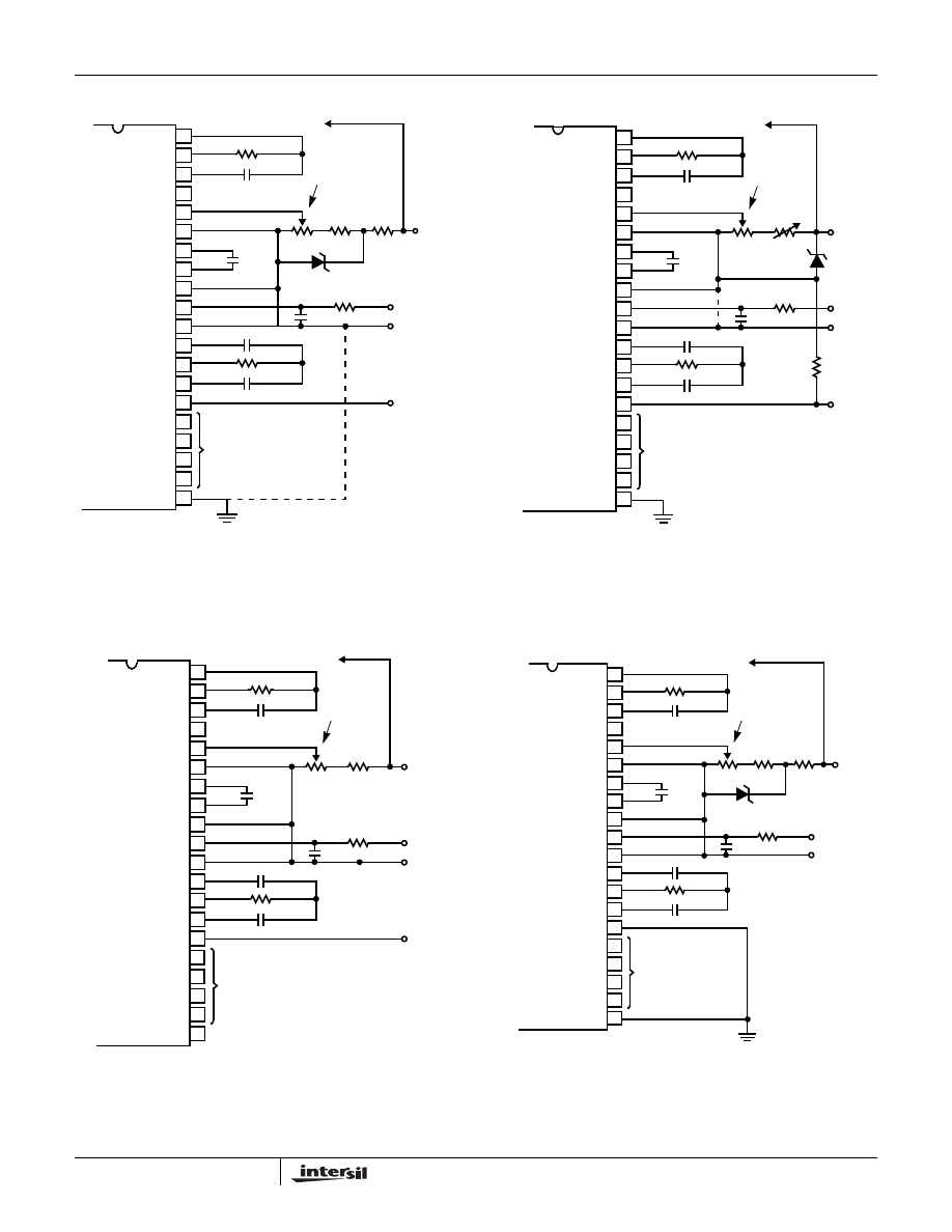
FIGURE 13. ICL7107 WITH AN EXTERNAL BAND-GAP
REFERENCE (1.2V TYPE)
FIGURE 14. ICL7107 WITH ZENER DIODE REFERENCE
FIGURE 15. ICL7106 AND ICL7107: RECOMMENDED
COMPONENT VALUES FOR 2V FULL SCALE
FIGURE 16. ICL7107 OPERATED FROM SINGLE +5V
Typical Applications
(Continued)
28
40
39
38
37
36
35
34
33
32
31
30
29
27
26
25
24
23
22
21
OSC 1
OSC 2
OSC 3
TEST
REF HI
REF LO
C
REF
C
REF
COMMON
IN HI
IN LO
A-Z
BUFF
INT
V
-
G2
C3
A3
G3
GND
100pF
TO PIN 1
SET V
REF
= 100mV
0.1
µ
F
0.01
µ
F
1M
Ω
100k
Ω
1k
Ω
10k
Ω
IN
+
47k
Ω
0.47
µ
F
TO DISPLAY
IN LO is tied to supply COMMON establishing the correct common mode
voltage. If COMMON is not shorted to GND, the input voltage may float
with respect to the power supply and COMMON acts as a pre-regulator
for the reference. If COMMON is shorted to GND, the input is single
ended (referred to supply GND) and the pre-regulator is overridden.
10k
Ω
1.2V (ICL8069)
V
-
V
+
-
0.22
µ
F
Since low TC zeners have breakdown voltages ~ 6.8V, diode must
be placed across the total supply (10V). As in the case of Figure 12,
IN LO may be tied to either COMMON or GND.
28
40
39
38
37
36
35
34
33
32
31
30
29
27
26
25
24
23
22
21
OSC 1
OSC 2
OSC 3
TEST
REF HI
REF LO
C
REF
C
REF
COMMON
IN HI
IN LO
A-Z
BUFF
INT
V -
G2
C3
A3
G3
GND
100pF
TO PIN 1
SET V
REF
= 100mV
0.1
µ
F
0.01
µ
F
1M
Ω
100k
Ω
1k
Ω
100k
Ω
IN
+
-
47k
Ω
0.22
µ
F
0.47
µ
F
TO DISPLAY
+5V
-5V
6.8V
28
40
39
38
37
36
35
34
33
32
31
30
29
27
26
25
24
23
22
21
OSC 1
OSC 2
OSC 3
TEST
REF HI
REF LO
C
REF
C
REF
COMMON
IN HI
IN LO
A-Z
BUFF
INT
V -
G2
C3
A3
G3
BP/GND
100pF
TO PIN 1
SET V
REF
= 1V
0.1
µ
F
0.01
µ
F
1M
Ω
100k
Ω
25k
Ω
24k
Ω
IN
+
-
470k
Ω
0.22
µ
F
0.047
µ
F
TO DISPLAY
V+
V-
28
40
39
38
37
36
35
34
33
32
31
30
29
27
26
25
24
23
22
21
OSC 1
OSC 2
OSC 3
TEST
REF HI
REF LO
C
REF
C
REF
COMMON
IN HI
IN LO
A-Z
BUFF
INT
V -
G2
C3
A3
G3
GND
100pF
TO PIN 1
SET V
REF
= 100mV
0.1
µ
F
0.01
µ
F
1M
Ω
100k
Ω
1k
Ω
10k
Ω
IN
+
-
47k
Ω
0.22
µ
F
0.47
µ
F
TO DISPLAY
An external reference must be used in this application, since the
voltage between V+ and V- is insufficient for correct operation of the
internal reference.
15k
Ω
1.2V (ICL8069)
+5V
ICL7106, ICL7107, ICL7107S
14
FIGURE 17. ICL7107 MEASUREING RATIOMETRIC VALUES
OF QUAD LOAD CELL
FIGURE 18. ICL7106 USED AS A DIGITAL CENTIGRADE
THERMOMETER
FIGURE 19. CIRCUIT FOR DEVELOPING UNDERRANGE AND
OVERRANGE SIGNAL FROM ICL7106 OUTPUTS
FIGURE 20. CIRCUIT FOR DEVELOPING UNDERRANGE AND
OVERRANGE SIGNALS FROM ICL7107 OUTPUT
Typical Applications
(Continued)
28
40
39
38
37
36
35
34
33
32
31
30
29
27
26
25
24
23
22
21
OSC 1
OSC 2
OSC 3
TEST
REF HI
REF LO
C
REF
C
REF
COMMON
IN HI
IN LO
A-Z
BUFF
INT
V -
G2
C3
A3
G3
GND
100pF
TO PIN 1
0.1
µ
F
100k
Ω
0.47
µ
F
TO DISPLAY
The resistor values within the bridge are determined by the desired
sensitivity.
V+
0.22
µ
F
47k
Ω
28
40
39
38
37
36
35
34
33
32
31
30
29
27
26
25
24
23
22
21
OSC 1
OSC 2
OSC 3
TEST
REF HI
REF LO
C
REF
C
REF
COMMON
IN HI
IN LO
A-Z
BUFF
INT
V -
G2
C3
A3
G3
BP
100pF
TO PIN 1
0.1
µ
F
0.01
µ
F
100k
Ω
100k
Ω
1M
Ω
9V
47k
Ω
0.22
µ
F
0.47
µ
F
TO BACKPLANE
TO DISPLAY
A silicon diode-connected transistor has a temperature coefficient of
about -2mV/
o
C. Calibration is achieved by placing the sensing
transistor in ice water and adjusting the zeroing potentiometer for a
000.0 reading. The sensor should then be placed in boiling water
and the scale-factor potentiometer adjusted for a 100.0 reading.
SCALE
FACTOR
ADJUST
100k
Ω
220k
Ω
22k
Ω
SILICON NPN
MPS 3704 OR
SIMILAR
ZERO
ADJUST
13
1
2
3
4
5
6
7
8
9
10
11
12
14
15
16
17
18
19
20
V+
D1
C1
B1
A1
F1
G1
E1
D2
C2
B2
A2
F2
E2
D3
B3
F3
E3
AB4
POL
28
40
39
38
37
36
35
34
33
32
31
30
29
27
26
25
24
23
22
21
OSC 1
OSC 2
OSC 3
TEST
REF HI
REF LO
C
REF
C
REF
COMMON
IN HI
IN LO
A-Z
BUFF
INT
V-
G2
C3
A3
G3
BP
O/RANGE
U/RANGE
CD4023 OR
74C10
CD4077
TO LOGIC
V
CC
V+
TO
LOGIC
V-
GND
O/RANGE
U/RANGE
CD4023 OR
74C10
TO LOGIC
V
CC
+5V
V-
33k
Ω
The LM339 is required to
ensure logic compatibility
with heavy display loading.
13
1
2
3
4
5
6
7
8
9
10
11
12
14
15
16
17
18
19
20
V+
D1
C1
B1
A1
F1
G1
E1
D2
C2
B2
A2
F2
E2
D3
B3
F3
E3
AB4
POL
28
40
39
38
37
36
35
34
33
32
31
30
29
27
26
25
24
23
22
21
OSC 1
OSC 2
OSC 3
TEST
REF HI
REF LO
C
REF
C
REF
COMMON
IN HI
IN LO
A-Z
BUFF
INT
V-
G2
C3
A3
G3
BP
12k
Ω
+
-
+
-
+
-
+
-
LM339
ICL7106, ICL7107, ICL7107S
15
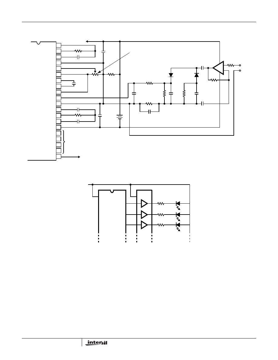
FIGURE 21. AC TO DC CONVERTER WITH ICL7106
FIGURE 22. DISPLAY BUFFERING FOR INCREASED DRIVE CURRENT
Typical Applications
(Continued)
28
40
39
38
37
36
35
34
33
32
31
30
29
27
26
25
24
23
22
21
OSC 1
OSC 2
OSC 3
TEST
REF HI
REF LO
C
REF
C
REF
COMMON
IN HI
IN LO
A-Z
BUFF
INT
V
-
G2
C3
A3
G3
BP
100pF
TO PIN 1
0.1
µ
F
100k
Ω
1k
Ω
22k
Ω
47k
Ω
0.22
µ
F
0.47
µ
F
TO BACKPLANE
TO DISPLAY
Test is used as a common-mode reference level to ensure compatibility with most op amps.
10
µ
F
9V
10
µ
F
470k
Ω
1
µ
F
4.3k
Ω
100pF
(FOR OPTIMUM BANDWIDTH)
1
µ
F
10k
Ω
10k
Ω
1N914
1
µ
F
0.22
µ
F
5
µ
F
CA3140
2.2M
Ω
+
-
100k
Ω
AC IN
SCALE FACTOR ADJUST
(V
REF
= 100mV FOR AC TO RMS)
+
-
ICL7107
130
Ω
130
Ω
130
Ω
LED
SEGMENTS
+5V
DM7407
ICL7106, ICL7107, ICL7107S
16
ICL7106, ICL7107, ICL7107S
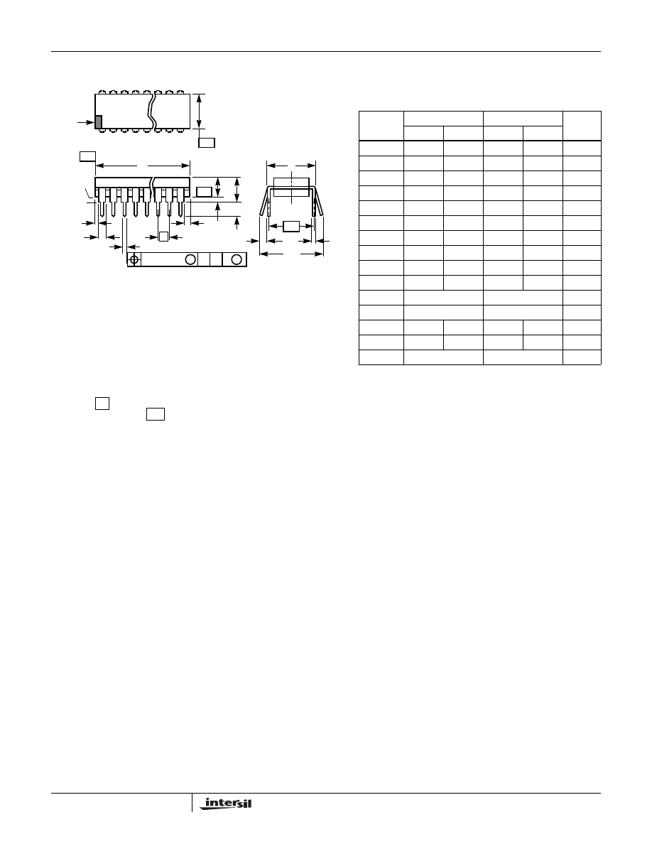
Dual-In-Line Plastic Packages (PDIP)
NOTES:
1. Controlling Dimensions: INCH. In case of conflict between English
and Metric dimensions, the inch dimensions control.
2. Dimensioning and tolerancing per ANSI Y14.5M-1982.
3. Symbols are defined in the “MO Series Symbol List” in Section 2.2
of Publication No. 95.
4. Dimensions A, A1 and L are measured with the package seated in
JEDEC seating plane gauge GS-3.
5. D, D1, and E1 dimensions do not include mold flash or protrusions.
Mold flash or protrusions shall not exceed 0.010 inch (0.25mm).
6. E and
are measured with the leads constrained to be per-
pendicular to datum
.
7. e
B
and e
C
are measured at the lead tips with the leads uncon-
strained. e
C
must be zero or greater.
8. B1 maximum dimensions do not include dambar protrusions. Dam-
bar protrusions shall not exceed 0.010 inch (0.25mm).
9. N is the maximum number of terminal positions.
10. Corner leads (1, N, N/2 and N/2 + 1) for E8.3, E16.3, E18.3, E28.3,
E42.6 will have a B1 dimension of 0.030 - 0.045 inch (0.76 - 1.14mm).
e
A
-C-
CL
E
e
A
C
e
B
e
C
-B-
E1
INDEX
1 2 3
N/2
N
AREA
SEATING
BASE
PLANE
PLANE
-C-
D1
B1
B
e
D
D1
A
A2
L
A1
-A-
0.010 (0.25)
C A
M
B S
E40.6
(JEDEC MS-011-AC ISSUE B)
40 LEAD DUAL-IN-LINE PLASTIC PACKAGE
SYMBOL
INCHES
MILLIMETERS
NOTES
MIN
MAX
MIN
MAX
A
-
0.250
-
6.35
4
A1
0.015
-
0.39
-
4
A2
0.125
0.195
3.18
4.95
-
B
0.014
0.022
0.356
0.558
-
B1
0.030
0.070
0.77
1.77
8
C
0.008
0.015
0.204
0.381
-
D
1.980
2.095
50.3
53.2
5
D1
0.005
-
0.13
-
5
E
0.600
0.625
15.24
15.87
6
E1
0.485
0.580
12.32
14.73
5
e
0.100 BSC
2.54 BSC
-
e
A
0.600 BSC
15.24 BSC
6
e
B
-
0.700
-
17.78
7
L
0.115
0.200
2.93
5.08
4
N
40
40
9
Rev. 0 12/93
17
All Intersil U.S. products are manufactured, assembled and tested utilizing ISO9000 quality systems.
Intersil Corporation’s quality certifications can be viewed at www.intersil.com/design/quality
Intersil products are sold by description only. Intersil Corporation reserves the right to make changes in circuit design, software and/or specifications at any time without
notice. Accordingly, the reader is cautioned to verify that data sheets are current before placing orders. Information furnished by Intersil is believed to be accurate and
reliable. However, no responsibility is assumed by Intersil or its subsidiaries for its use; nor for any infringements of patents or other rights of third parties which may result
from its use. No license is granted by implication or otherwise under any patent or patent rights of Intersil or its subsidiaries.
For information regarding Intersil Corporation and its products, see www.intersil.com
ICL7106, ICL7107, ICL7107S
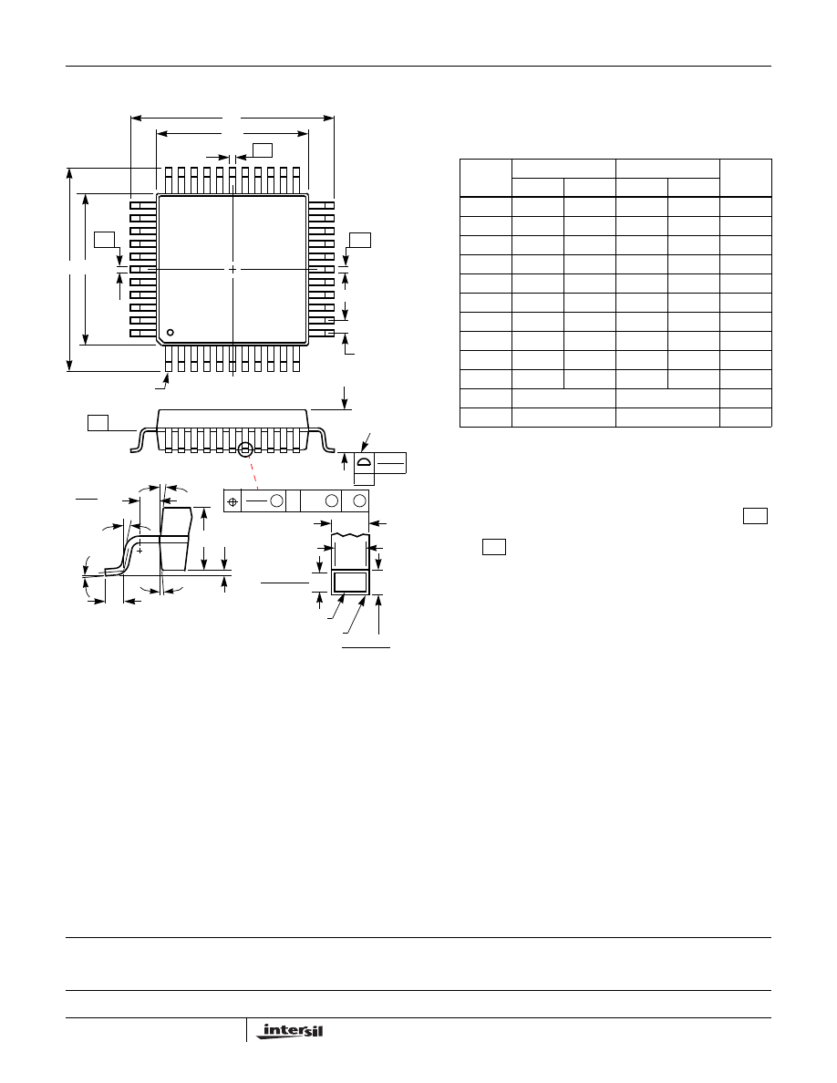
Metric Plastic Quad Flatpack Packages (MQFP)
D
D1
E E1
-A-
PIN 1
A2 A1
A
12
o
-16
o
12
o
-16
o
0
o
-7
o
0.40
0.016 MIN
L
0
o
MIN
PLANE
b
0.005/0.009
0.13/0.23
WITH PLATING
BASE METAL
SEATING
0.005/0.007
0.13/0.17
b1
-B-
e
0.008
0.20
A-B
S
D
S
C
M
0.076
0.003
-C-
-D-
-H-
Q44.10x10
(JEDEC MS-022AB ISSUE B)
44 LEAD METRIC PLASTIC QUAD FLATPACK PACKAGE
SYMBOL
INCHES
MILLIMETERS
NOTES
MIN
MAX
MIN
MAX
A
-
0.096
-
2.45
-
A1
0.004
0.010
0.10
0.25
-
A2
0.077
0.083
1.95
2.10
-
b
0.012
0.018
0.30
0.45
6
b1
0.012
0.016
0.30
0.40
-
D
0.515
0.524
13.08
13.32
3
D1
0.389
0.399
9.88
10.12
4, 5
E
0.516
0.523
13.10
13.30
3
E1
0.390
0.398
9.90
10.10
4, 5
L
0.029
0.040
0.73
1.03
-
N
44
44
7
e
0.032 BSC
0.80 BSC
-
Rev. 2 4/99
NOTES:
1. Controlling dimension: MILLIMETER. Converted inch
dimensions are not necessarily exact.
2. All dimensions and tolerances per ANSI Y14.5M-1982.
3. Dimensions D and E to be determined at seating plane
.
4. Dimensions D1 and E1 to be determined at datum plane
.
5. Dimensions D1 and E1 do not include mold protrusion.
Allowable protrusion is 0.25mm (0.010 inch) per side.
6. Dimension b does not include dambar protrusion. Allowable
dambar protrusion shall be 0.08mm (0.003 inch) total.
7. “N” is the number of terminal positions.
-C-
-H-

This datasheet has been download from:
Datasheets for electronics components.
Wyszukiwarka
Podobne podstrony:
ICL7106 7107
icl7106 i 7107
7107
Kolejny miernik na ICL7107 i wyświetlaczach LED wspólna anoda schemat
Miliwoltomierz cyfrowy z przetwornikiem ICL7107
NE035 TERMOMETR CYFROWY 20°C÷ 99°C LEDICL 7107
ICL 7107 i ICL 7106
icl7107 7106
7107
7107
Kolejny miernik na ICL7107 i wyświetlaczach LED wspólna anoda, schemat
7107
7107
ICL7107
ICL7107
icl 7107 ZKGZ6VT7REFRZ4JYHH3H5O6BC2J2XD4R7DMPMMY
icl7106
więcej podobnych podstron