
Developer Note
© Apple Computer, Inc. 1997
Developer Note
Power Macintosh 5500 and 6500
Computers

ð
Apple Computer, Inc.
© 1997 Apple Computer, Inc.
All rights reserved.
No part of this publication may be
reproduced, stored in a retrieval
system, or transmitted, in any form or
by any means, mechanical, electronic,
photocopying, recording, or otherwise,
without prior written permission of
Apple Computer, Inc., except to make a
backup copy of any documentation
provided on CD-ROM. Printed in the
United States of America.
The Apple logo is a trademark of
Apple Computer, Inc.
Use of the “keyboard” Apple logo
(Option-Shift-K) for commercial
purposes without the prior written
consent of Apple may constitute
trademark infringement and unfair
competition in violation of federal and
state laws.
No licenses, express or implied, are
granted with respect to any of the
technology described in this book.
Apple retains all intellectual property
rights associated with the technology
described in this book. This book is
intended to assist application
developers to develop applications only
for Apple-labeled or Apple-licensed
computers.
Every effort has been made to ensure
that the information in this manual is
accurate. Apple is not responsible for
printing or clerical errors.
Apple Computer, Inc.
1 Infinite Loop
Cupertino, CA 95014
408-996-1010
Apple, the Apple logo, AppleLink,
Apple SuperDrive, GeoPort,
LaserWriter, LocalTalk, Macintosh,
Macintosh Quadra, Performa,
PlainTalk, and Power Macintosh are
trademarks of Apple Computer, Inc.,
registered in the United States and
other countries.
QuickDraw and QuickDraw 3D are
trademarks of Apple Computer, Inc.
Adobe Illustrator and PostScript are
trademarks of Adobe Systems
Incorporated, which may be registered
in certain jurisdictions.
Helvetica and Palatino are registered
trademarks of Linotype Company.
ITC Zapf Dingbats is a registered
trademark of International Typeface
Corporation.
NuBus is a trademark of Texas
Instruments.
PowerPC is a trademark of
International Business Machines
Corporation, used under license
therefrom.
The word SRS is a registered trademark
of SRS Labs, Inc.
Simultaneously published in the United
States and Canada.
LIMITED WARRANTY ON MEDIA AND
REPLACEMENT
If you discover physical defects in the
manual or in the media on which a software
product is distributed, ADC will replace the
media or manual at no charge to you
provided you return the item to be replaced
with proof of purchase to ADC.
ALL IMPLIED WARRANTIES ON THIS
MANUAL, INCLUDING IMPLIED
WARRANTIES OF MERCHANTABILITY
AND FITNESS FOR A PARTICULAR
PURPOSE, ARE LIMITED IN DURATION
TO NINETY (90) DAYS FROM THE DATE
OF THE ORIGINAL RETAIL PURCHASE
OF THIS PRODUCT.
Even though Apple has reviewed this
manual, APPLE MAKES NO WARRANTY
OR REPRESENTATION, EITHER EXPRESS
OR IMPLIED, WITH RESPECT TO THIS
MANUAL, ITS QUALITY, ACCURACY,
MERCHANTABILITY, OR FITNESS FOR A
PARTICULAR PURPOSE. AS A RESULT,
THIS MANUAL IS SOLD “AS IS,” AND
YOU, THE PURCHASER, ARE ASSUMING
THE ENTIRE RISK AS TO ITS QUALITY
AND ACCURACY.
IN NO EVENT WILL APPLE BE LIABLE
FOR DIRECT, INDIRECT, SPECIAL,
INCIDENTAL, OR CONSEQUENTIAL
DAMAGES RESULTING FROM ANY
DEFECT OR INACCURACY IN THIS
MANUAL, even if advised of the possibility
of such damages.
THE WARRANTY AND REMEDIES SET
FORTH ABOVE ARE EXCLUSIVE AND IN
LIEU OF ALL OTHERS, ORAL OR
WRITTEN, EXPRESS OR IMPLIED. No
Apple dealer, agent, or employee is
authorized to make any modification,
extension, or addition to this warranty.
Some states do not allow the exclusion or
limitation of implied warranties or liability
for incidental or consequential damages, so
the above limitation or exclusion may not
apply to you. This warranty gives you
specific legal rights, and you may also have
other rights which vary from state to state.

iii
Contents
About This Note
ix
Supplemental Reference Documents
x
Apple Developer World Web Site
Introduction
1
Comparison With Macintosh Performa 6400 Computer
Rear Panel Subwoofer Volume Control
Built-in Video and Graphics Features

iv
Architecture
15
I/O Features
23
External Video Connection for Tower Enclosures

v
Expansion Features
41
The PCI Bus Communications Slot
PCI Bus Communications Slot Connector
Expansion Bay for SCSI Devices
Software Components for the 2D and 3D Hardware
Graphics Accelerator
71
QuickDraw 2D Acceleration Extension
QuickDraw 3D Acceleration Extension
Deviations from Rave API Methods
QuickTime Acceleration Extension
77

vi

vii
Figures and Tables
Introduction
1
Front view of the computer
6
Back view of the computer
7
Voltage switch on the tower enclosure
13
Comparison with the Macintosh Performa 6400 series
computer
4
Architecture
15
System block diagram
17
I/O Features
23
Serial port sockets
24
Maximum dimensions of the hard disk
28
Serial port signals
24
ADB connector pin assignments
25
Pin assignments on the floppy disk connector
26
Pin assignments on the ATA (IDE) hard disk connector
29
Signals on the ATA (IDE) hard disk connector
30
Specifications of the CD-ROM drive
31
Pin assignments for the SCSI connectors
31
Reset and NMI key combinations
35
Pin assignments for the external video connector
36
Maximum pixel depths for video monitors
36
Tower enclosure video input and graphics acceleration display
modes
37
All-in-one enclosure video input and graphics acceleration display
modes
38
Expansion Features
41
Dimensions of the RAM DIMM
49
DAV connecting cable
55
Location of the DAV connector
55
Orientation of the DAV connector
56
Video data timing
60
Communications slot card compatibility
63
Universal modem card for communications slot
64
Tower enclosure expansion bay
67
Maximum usable area for device opening on bay cover
68

viii
Memory sizes and configurations for single bank DIMMS
42
Pin assignments on the RAM DIMM connectors
43
RAM DIMM signals
46
Address multiplexing modes for various DRAM devices
47
Address multiplexing in noninterleaved banks
47
Pin and signal assignments for L2 cache DIMM connector
50
Signal descriptions for L2 cache DIMM connector
51
PCI signals
53
Pin assignments on the DAV connector
57
Descriptions of the signals on the DAV connector
58
DAV signal levels
59
Pin assignments for the PCI bus communications slot
connector
61
Pin assignments for a universal serial modem card
65
Pin assignments for the expansion bay power connector
69
Software Components for the 2D and 3D Hardware Graphics
Accelerator
71
ATi3D extension
kQATag_TextureFilter
setting
interpretation
74
Memory allocation for a full-screen 3D window
76
Memory allocation for a half-screen 3D window
76

ix
P R E F A C E
About This Note
This developer note describes the main logic board used in the Power
Macintosh 5500 and 6500 computers and emphasizes features that are new or
different from previous Macintosh models. It is intended to help experienced
Macintosh hardware and software developers design compatible products. If
you are unfamiliar with Macintosh computers or would simply like more
technical information, you may wish to read the related technical manuals
listed in the section “Supplemental Reference Documents.”
Contents of This Note
0
The information is arranged in five chapters and an index:
■
Chapter 1, “Introduction,” gives a summary of the features of the logic
board, describes the physical appearance of the tower enclosure, and lists
the available configurations and options. This chaper also includes a
section that describes the compatibility issues that hardware and software
developers need to be aware of to take advantage of the logic board
features.
■
Chapter 2, “Architecture,” describes the internal organization of the
computer. It includes a block diagram and descriptions of the main
components of the logic board.
■
Chapter 3, “I/O Features,” describes the built-in input/output (I/O)
devices and the external I/O ports. It also describes the built-in monitor
configuration of the InstaTower and external video monitors that can be
used with the computer.
■
Chapter 4, “Expansion Features,” describes the expansion slots on the logic
board. This chapter provides guidelines for designing cards for the I/O
expansion slot and brief descriptions of the expansion modules for the
other slots.
■
Chapter 5, “Software Components for the 2D and 3D Hardware Graphics
Accelerator,” describes the Macintosh system extensions that control the
2D and 3D hardware acceleration features of the ATI264GT graphics
controller on the logic board.
Supplemental Reference Documents
0
To supplement the information in this developer note, developers should
have copies of the appropriate Motorola reference books for the

x
P R E F A C E
PowerPC™ 603e microprocessor. Software developers should have a copy of
Motorola’s
PowerPC Programmer’s Reference Manual.
Hardware developers
should have copies of Motorola’s
PowerPC 603 RISC Microprocessor User’s
Manual.
For additional information about the digital data format used in the video
input module, refer to
Power Macintosh DAV Interface for PCI Expansion Cards.
For information about the digital video interface, refer to the
SAA7140 Philips
Desktop Video Handbook
.
Developers may also need copies of the appropriate Apple reference books.
You should have the relevant books of the
Inside Macintosh
series
.
Developers
interested in taking advantage of the 3D graphics acceleration features built
into the logic board should have
3D Graphics Programming With QuickDraw
3D.
You should also have
Designing PCI Cards and Drivers for Power Macintosh
Computers
. These books are available in technical bookstores and through the
Apple Developer Catalog.
The
Apple Developer Catalog
0
The
Apple Developer Catalog
(ADC) is Apple Computer’s worldwide source for
hundreds of development tools, technical resources, training products, and
information for anyone interested in developing applications on Apple
computer platforms. Customers receive the
Apple Developer Catalog
featuring
all current versions of Apple development tools and the most popular
third-party development tools. ADC offers convenient payment and shipping
options, including site licensing.
To order products or to request a complimentary copy of the
Apple Developer
Catalog
, contact
Apple Developer Catalog
Apple Computer, Inc.
P.O. Box 319
Buffalo, NY 14207-0319
Telephone
1-800-282-2732 (United States)
1-800-637-0029 (Canada)
1-716-871-6555 (International)
Fax
1-716-871-6511
AppleLink
ORDER.ADC
Internet
http://www.devcatalog.apple.com

xi
P R E F A C E
Apple Developer World Web Site
0
The Apple Developer World Wide Web site is the one-stop source for finding
technical and marketing information specifically for developing successful
Macintosh-compatible software and hardware products. Developer World is
dedicated to providing developers with up-to-date Apple documentation for
existing and emerging Macintosh technologies. Developer World can be
reached at
http://www.devworld.apple.com
Conventions and Abbreviations
0
This developer note uses the following typographical conventions and
abbreviations.
Typographical Conventions
0
New terms appear in
boldface
where they are first defined.
Computer-language text—any text that is literally the same as it appears in
computer input or output—appears in
Courier
font.
Hexadecimal numbers are preceded by a dollar sign ($). For example, the
hexadecimal equivalent of decimal 16 is written as $10.
Note
A note like this contains information that is interesting but not essential
for an understanding of the text.
◆
IMPORTANT
A note like this contains important information that you should read
before proceeding.
▲
▲
W A R N I N G
A note like this directs your attention to something that could cause
damage or result in a loss of data.
▲

xii
P R E F A C E
Standard Abbreviations
0
When unusual abbreviations appear in this book, the corresponding terms are
also spelled out. Standard units of measure and other widely used
abbreviations are not spelled out. Here are the standard units of measure
used in this developer note:
Here are other abbreviations used in this developer note:
A
amperes
mA
milliamperes
dB
decibels
µ
A
microamperes
GB
gigabytes
MB
megabytes
Hz
hertz
MHz
megahertz
in.
inches
mm
millimeters
k
1000
ms
milliseconds
K
1024
µ
s
microseconds
KB
kilobytes ns
nanoseconds
kg
kilograms
Ω
ohms
kHz
kilohertz
sec.
seconds
k
Ω
kilohms
V
volts
lb.
pounds
W
watts
$n hexadecimal
value
n
AC
alternating current
ADB
Apple Desktop Bus
AV
audiovisual
AWACS
audio waveform amplifier and converter for sound
CD-ROM
compact disc read-only memory
CLUT
color lookup table
DAV
digital audio video
DESC
digital video decoder and scaler
DIMM
dual inline memory module
DMA
dynamic memory access
DRAM
dynamic random-access memory
DVA
digital video application
EDO
extended data out DRAM device type
EMI
electromagnetic interference
FPU
floating-point unit
IC
integrated circuit
IDE
integrated device electronics
IIC
inter-integrated circuit (an internal control bus)

xiii
P R E F A C E
I/O
input/output
IR
infrared
LS TTL
low-power Schottky TTL (a standard type of device)
MMU
memory management unit
MOS
metal-oxide semiconductor
NTSC
National Television Standards Committee (the standard system
used for broadcast TV in North America and Japan)
NMI
nonmaskable interrupt
PAL
Phase Alternating Line system (the standard for broadcast TV
in most of Europe, Africa, South America, and southern Asia)
PCI
Peripheral Component Interconnect
PDS
processor-direct slot
PWM
pulse-width modulation
RAM
random-access memory
RAVE
rendering acceleration virtual engine
RGB
a video signal format with separate red, green, and blue
components
RISC
reduced instruction set computing
RMS
root-mean-square
ROM
read-only memory
SANE
Standard Apple Numerics Environment
SCSI
Small Computer System Interface
SCC
serial communications controller
SECAM
the standard system used for broadcast TV in France and the
former Soviet countries
SGRAM
synchronous graphics random access memory
SIMM
single inline memory module
S-video
a type of video connector that keeps luminance and
chrominance separate; also called a Y/C connector
SWIM
Super Woz Integrated Machine, a custom IC that controls the
floppy disk interface
TTL
transistor-transistor logic (a standard type of device)
VCR
video-cassette recorder
VLSI
very large scale integration
VRAM
video RAM; used for display buffers
Y/C
a type of video connector that keeps luminance and
chrominance separate; also called an S-video connector
YUV
a video signal format with separate luminance and
chrominance components


C H A P T E R 1
Introduction
1
Figure 1-0
Listing 1-0
Table 1-0

C H A P T E R 1
Introduction
2
Summary of Features
The main logic board in the Power Macintosh 5500 and 6500 computers is a plug-in logic
board that incorporates a PowerPC™ 603e microprocessor, a second-level (L2) cache
expansion slot, one or two Peripheral Component Interconnect (PCI) card expansion
slots, enhanced AV features (audio and video input and output), and a PCI-based
communications slot (comm slot II). The logic board is housed in a two-slot tower
enclosure like the Macintosh Performa 6400 enclosure and an all-in-one enclosure like
the Power Macintosh 5400. The tower enclosure features easy access, an expansion bay,
and a built-in subwoofer.
Note
The enclosures, although simular to previous Macintosh enclosures,
incorporate mechanical design changes that provide the necessary
cooling to support the higher speed PowerPC processors used on the
new logic board.
◆
Summary of Features
1
Here is a summary of the hardware features of the Power Macintosh 5500 and 6500
computers. Each feature is described more fully later in this note.
■
Microprocessor: PowerPC 603e microprocessor running at 175 MHz, 200 MHz,
225 MHz, and 250 MHz.
■
RAM: 0 MB on the main logic board; expandable to 128 MB using 168-pin
JEDEC-standard 5-volt buffered EDO (extended data out) DIMM (dual inline memory
module) devices with 2K refresh rate. Two DIMM slots are provided for DRAM
expansion.
■
ROM: 4 MB soldered on main logic board; 64-bit ROM data bus width.
■
Cache: 256 KB second-level (L2) cache on a 160-pin DIMM card (optional)
■
Video display modes supported on built-in monitor port: 640 by 480, 800 by 600, and
832 by 624 at 32 bits per pixel; 1024 by 768 and 1152 by 870 at 16 bits per pixel;
1280 by 1024 at 8 bits per pixel; 2 MB synchronous graphics RAM (SGRAM) frame
buffer on the main logic board.
■
Built-in 2D and 3D hardware graphics acceleration. Software support through
Macintosh QuickDraw 3D and QuickDraw 3D RAVE (rendering acceleration virtual
engine) APIs. For more information about the 3D graphics acceleration features see,
Chapter 5, “Software Components for the 2D and 3D Hardware Graphics Accelerator.”
■
Built-in YUV and MPEG scaler.
■
Video input: optional video-in card allows video input through an RCA or S-Video
connector; a 60-pin DAV connector on the video-in card supports an optional MJPEG
video card for real-time video capture, display, and overlay.
■
Video output: optional cards provide video output.
■
Video display mirror output on all-in-one enclosures.

C H A P T E R 1
Introduction
Summary of Features
3
■
Sound: 16 bits/channel stereo input, SRS® stereo surround-sound output, external
jack for sound in, front jack for headphones, rear jack for stereophonic speakers, one
built-in speaker/subwoofer in tower enclosures, stereo speakers on all-in-one
enclosures.
■
TV/FM receiver: optional internal TV/FM tuner with F-type antenna connectors.
■
Remote control for TV/FM tuner and computer power on/off: infrared.
■
Hard disks: one internal 3.5-inch IDE hard disk with 2 GB or larger capacity and an
external SCSI port for additional SCSI devices. PIO, singleword DMA, and multiword
DMA data transfers are supported.
■
Expansion bay (tower enclosure): allows adding an internal 5.25-inch or 3.5-inch SCSI
device. Some models may include an optional Iomega Zip drive.
■
Floppy disk: one internal 1.4 MB Apple SuperDrive.
■
CD-ROM drive: internal 12X-speed CD-ROM drive.
■
Processor bus: 64-bit wide, 50 MHz, supporting split address and data tenures.
■
Standard Macintosh I/O ports: two serial ports, sound input and output jacks, a SCSI
port, and an ADB port.
■
GeoPort: supported on both the modem port and the printer port.
■
PCI-based communications slot (comm slot II): 112-pin connector accepts an optional
modem or Ethernet interface. This is the same type of communications slot found in
the Power Macintosh 5400 and Performa 6400 computers.
■
PCI card expansion slots: accepts two 7-inch PCI cards in tower enclosure with
expansion/riser card and one 7-inch PCI card in the all-in -one enclosure; 15 watts
maximum each card.
■
Power switch: soft power controlled from keyboard and infrared remote control.
■
Voltage switch (tower enclosure only): allows selection of either 115 for voltages of
100–130 V or 230 for voltages of 200–230 V depending on the voltage which you will
be connecting to. The voltage selection must be set manually.
■
Case design: tower case design like that used for the Macintosh Performa 6400
computer with an easy-to-remove front panel and expansion bay panel. The tower
case also incorporates a built-in subwoofer. All-in-one enclosure like that used for the
Power Macintosh 5400 computer.
■
Fan speed control: In the all-in-one eclosure, the speed of the fan is thermally
controlled and is automatically set to the lowest possible speed to minimize noise. The
fan speed varies according to the temperature inside the enclosure. For additional
cooling, the PowerPC processor also has a small fan.
■
Energy saving: sleep, startup, and shutdown scheduling can be controlled with an
Energy Saver control panel.

C H A P T E R 1
Introduction
4
Comparison With Macintosh Performa 6400 Computer
Comparison With Macintosh Performa 6400 Computer
1
The main logic board in the Power Macintosh 6500 is based on the logic board in the
Macintosh Performa 6400. However, several performance improvements have been
incorporated into the design. Table 1-1 compares the features of these computers.
Table 1-1
Comparison with the Macintosh Performa 6400 series computer
Features
Macintosh Performa 6400
Power Macintosh 6500 main
logic board
Processor type
PowerPC 603e
PowerPC 603e
Processor speed
160 MHz, 180 MHz, and
200 MHz
175 MHz, 200 MHz,
225 MHz, and 250 MHz
Cache
256 KB level-2 cache
(optional)
256 KB level-2 cache
(optional)
Amount of RAM
16 MB–136 MB (8 MB on
main logic board)
16 MB–128 MB (0 MB on
main logic board)
RAM expansion
2 168-pin 5-volt fast-paged
DIMMs
2 168-pin 5-volt EDO DIMMs
Memory bus
64 bits, 40 MHz
64 bits, 50 MHz
Video RAM
1 MB (DRAM)
2 MB (SGRAM)
Video input
Optional card for video
input, capture, and overlay
Optional card for video
input, capture, and overlay
Video output
Built-in video supports up
to 1024-by-768 pixel
resolution at 8 bits per pixel,
VGA and SVGA
Built-in video supports up
to 1280-by-1024 pixel
resolution at 16 bits per
pixel, VGA and SVGA
Graphics
acceleration
None
2D and 3D built-in
hardware graphics
acceleration.
Sound capabilities
8 or 16 bits/channel; stereo
in, stereo record, stereo out;
SRS surround-sound mode
8 or 16 bits/channel; stereo
in, stereo record, stereo out;
SRS surround-sound mode
Remote control
Built-in IR receiver for
optional TV/FM tuner card
Built-in IR receiver for
optional TV/FM tuner card
Floppy disk drive
1, internal
1, internal
ADB ports
1
1
Internal hard disk
1 (IDE)
1 (IDE)
Internal CD-ROM
1
1

C H A P T E R 1
Introduction
External Features
5
External Features
1
The main logic board is designed to work in an all-in-one enclosure like the Power
Maintosh 5400 enclosure and in a two-slot tower enclosure like that of the Macintosh
Performa 6400. The all-in-one model is called the Power Macintosh 5500 computer and
the two-slot tower is the Power Macintosh 6500 computer.
This section describes the features of the tower enclosure of th ePower Macintosh 6500.
For information about external features of the all-in-one enclosure, see the Power
Macintosh 5400 Developer Note.
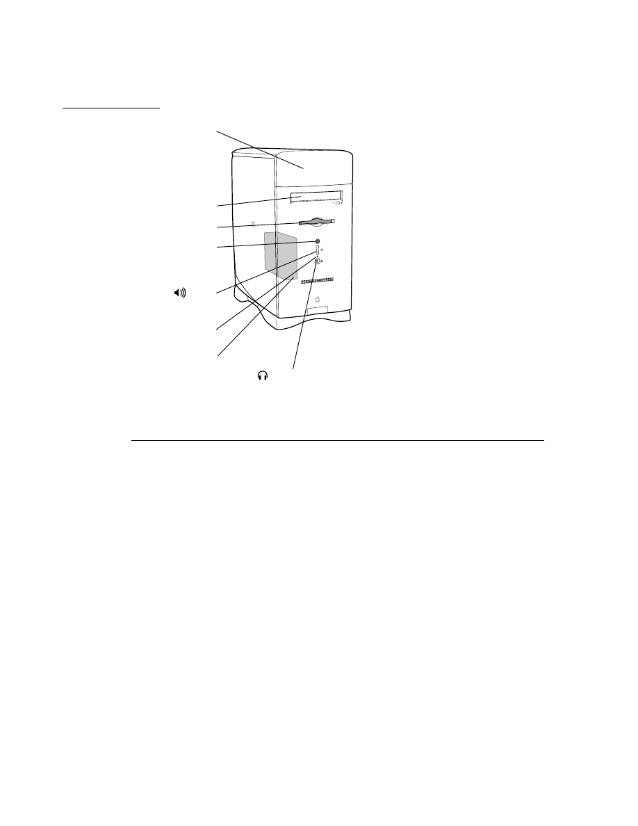
Front View
1
Figure 1-1 is a front view of a Power Macintosh 6500 tower enclosure. The front view
shows the location of the expansion bay, the openings for the CD-ROM drive and floppy
disk, the CD-ROM open and close button, the IR sensor for the remote control, the push
button that controls the sound level, the power-on light, and the headphone jack.
continued
Internal SCSI
expansion bay
1, for one 5.25-inch SCSI
device
Tower enclosure has 1, for
one 3.5-inch or 5.25-inch
SCSI device (some models
include a Zip drive);
all-in-one enclosure does not
have expansion bay
External SCSI ports
1
1
Communications slot
1, for optional modem or
Ethernet interface (PCI bus
configuration)
1, for optional modem or
Ethernet interface (PCI bus
configuration)
Expansion slot
2 PCI slots for 7-inch cards
1 (all-in-one) or 2 (tower)
PCI slots for 7-inch cards
DMA I/O
10 DMA channels
10 DMA channels
Serial ports
2, LocalTalk and GeoPort
supported
2, LocalTalk and GeoPort
supported
Table 1-1
Comparison with the Macintosh Performa 6400 series computer (continued)
Features
Macintosh Performa 6400
Power Macintosh 6500 main
logic board
C H A P T E R 1
Introduction
6
External Features
Figure 1-1
Front view of the Power Macintosh 6500 computer
Back View
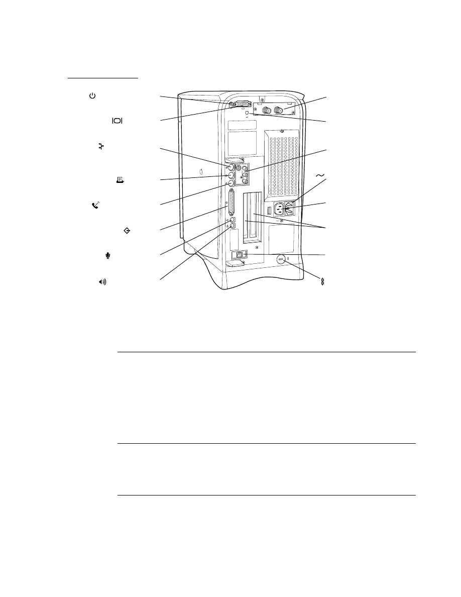
1
The back panel includes the power socket, the monitor power socket, the reset button,
the I/O ports, and openings for I/O access to the expansion modules: the I/O expansion
card, the communications card, and the video input card.
Figure 1-2 shows the back view of a Power Macintosh 6500 computer.
Floppy disk drive
Expansion bay
Behind the front panel
there is an expansion
bay for an optional
5-1/4" storage device
(1.72" high)
Internal hard disk drive
Power-on light
CD-ROM drive
Sound
control button
Infrared
remote control sensor
Headphone jack
C H A P T E R 1
Introduction
External Features
7
Figure 1-2
Back view of the computer
Access to the Logic Board
1
The logic board can be removed from the case so that the user can add expansion RAM,
second-level L2 cache, or plug-in I/O expansion cards. The rear fence of the logic board
is connected to the back panel. On the tower enclosure, the back panel is secured to the
computer chassis by two screws at the side of the plastic tabs on the back panel. After
removing the two screws, you can gently pull on the two tabs to remove the logic board
from the internal logic board connector and chassis.
Front Panel Push Button
1
The Macintosh Performa tower enclosure has a push button on the front panel to control
the sound volume of the internal speaker.
Rear Panel Subwoofer Volume Control
1
A knob located below the monitor port on the back of the tower enclosure controls the
low-frequency volume of the internal speaker when the computer is in subwoofer mode
(when external speakers are connected to the rear speaker jack).
Monitor power socket
Standby power button
SCSI port
External modem port
Printer port
Sound output port
Apple Desktop Bus
(ADB) port
Sound input port
Power socket
Security lock port
TV/FM tuner card (optional)
Monitor port
Subwoofer volume control
PCI card access covers (2)
Internal modem card (optional)
Video input card (optional)

C H A P T E R 1
Introduction
8
Optional Features
Power On and Off
1
The user can turn the power on and off by pressing one of two buttons:
■
the Power key on the keyboard
■
the Power key on the remote control
If files are still open when the user attempts to turn off the computer by using either one
of the Power keys or the Shut Down menu item, the system displays an alert box
warning the user that files are open and should be closed to avoid loss of data.
Optional Features
1
Several features of the logic board are implemented as plug-in modules available either
as a configuration option at the time of purchase or as a later upgrade. The modules are
designed so that they can be installed by the user.
TV and FM Radio Tuner
1
The TV and FM Radio tuner module turns the computer into a television and FM radio
receiver, complete with remote control. The features of the TV tuner module are the same
as those for the TV tuner in the Power Macintosh 5400 and Macintosh Performa 6400
computers. The TV picture is in its own window on the desktop, and the TV signal is
carried in YUV format for improved picture clarity.
The features of the TV tuner module are
■
ability to remotely tune 181 broadcast and cable channels (U.S. version)
■
coaxial connector for TV antenna or cable input (F-type connector in U.S. and
Japanese versions; IEC-type connector in Europe)
■
TV picture in a resizable and movable window
■
YUV format for improved clarity (see sidebar)
■
support for closed captioning and teletext
■
software password protection
■
automatic and manual channel programming
■
single remote control for TV and for playback of audio CDs
The features of the FM radio tuner are
■
ability to receive and display FM radio frequencies
■
scan and search stations up and down the frequency spectrum
■
step frequency
■
DX mode to tune out harmonic spillover from other stations
■
stereo/mono station indicator

C H A P T E R 1
Introduction
Optional Features
9
■
preset station programming
For more information about the the TV and FM Radio tuner module, see the Macintosh
Performa 6400 Developer Note.
Video Input
1
The video input card accepts video from an external source and displays it in a window
on the computer’s display. The features of the video input card are
■
acceptance of video input in NTSC, PAL, or SECAM format
■
connectors for stereo sound, composite video, and S-video (Y/C)
■
video display in a 320-by-240 pixel window
■
pixel expansion for 640-by-480 pixel maximum display
■
video overlay capability
■
YUV format for digital video input
■
a digital audio video (DAV) connector for adding a video processor on a PCI
expansion card
The video input card provides AV features similar to those of the Macintosh
Quadra 660AV, with one key improvement. Whereas the Macintosh Quadra 660AV
digitizes color video using a 16-bit RGB format, the video input card uses a digital YUV
format. Because a standard television signal has more information in its chrominance
channel than in its luminance channels, digitizing the video signal as YUV format results
in a clearer picture.
The video input card can accept video input from either an external device such as a
VCR or camcorder, or from the internal TV tuner module. The external device can be
connected to the video input card through either the composite video connector or the
S-video connector.
The default window size is 320 by 240 pixels; the user can resize the window up to 640
by 480 pixels—the full screen on a 14-inch monitor. The large image uses pixel expansion
of the 320-by-240 pixel image.
The video input card plugs into a dedicated slot on the main logic board. The slot
connector is a 60-pin microchannel connector. The module fits only its proper slot and
only in the proper orientation so that the user can safely install the video input card.
The video input card has a separate connector called the DAV (digital audio video)
connector. The DAV connector makes the digitized video data available to a card in the
PCI I /O expansion slot. Such a card can contain a hardware video compressor or other
video processor. The Avid Cinema card is a PCI video compressor card solution
developed for the Macintosh Performa 6400 and can be used with the logic board in the
Power Macintosh 5500 and 6500 computers. For more information about the DAV
implementation, see the section “The DAV Connector” beginning on page 54.

C H A P T E R 1
Introduction
10
Compatibility Issues
Communications
1
The logic board has a communications slot that allows the computer to support a
communications module without occupying the PCI expansion slot. A communications
card can be installed by either the user or the dealer.
The communications slot uses a PCI bus, rather than the 680xx bus. The communications
slot is also referred to as comm slot II to differentiate it from comm slot I in the Power
Macintosh 5200 and 6200 series of computers. The following cards are supported in the
comm slot II connector:
■
the 10BaseT (twisted pair) ethernet card
■
the 10Base2 (thin coax) ethernet card
■
the AAUI (Apple standard) ethernet card
■
the 28.8 or 33.6 bps fax/data modem card
Expansion Bay
1
The expansion bay in the tower enclosure includes data and power connectors for
adding another SCSI device. The bay is configured to support one 3.5-inch or 5.25-inch
device. Some configurations of the tower enclosure include an optional Zip drive in the
expansion bay. For additional information about the expansion bay mechanical and
electrical characteristics, see “Expansion Bay for SCSI Devices” beginning on page 66.
Compatibility Issues
1
Power Macintosh 5500 and 6500 computers incorporate several changes from earlier
desktop models. This section describes key issues you should be aware of to ensure that
your hardware and software work properly with the Power Macintosh 5500 and 6500
models.
Communications Slot
1
The communications slot is a PCI bus compatible slot (comm slot II) and is in general not
compatible with communication cards for the Macintosh LC family of computers, the
Macintosh Quadra 630 computer, or cards that operate in the communications slot
(comm slot I) in Power Macintosh 5200 and 6200 computers. The exception is that cards
that do not use the bus, such as serial modem cards, can be designed to work in both
comm slot I and comm slot II. For more information about designing serial modem cards
that are compatible with both communications slots, see “The PCI Bus Communications
Slot” beginning on page 60. The comm slot on the Power Macintosh 6500 asnd 5500 logic
board is the same as the comm slot in the Macintosh Performa 6400 and Power
Macintosh 5400 computers.

C H A P T E R 1
Introduction
Compatibility Issues
11
DAV Slot
1
The digital audio video (DAV) connector on the video in card is compatible with the
Macintosh Performa 6400 and Power Macintosh 5400, 7600, and 8500 computers.
However, it is not compatible with the DAV slot in the Macintosh Quadra 660AV,
Macintosh Quadra 840AV, and Power Macintosh 6100, 7100, and 8100 computers, nor is
it direct plug-in compatible with the DVA (digital video application) slot in the Power
Macintosh 5200 and 6200 computers. The DAV slot is a 60-pin slot with additional
signals and capabilities. For additional information about the DAV slot, see “The DAV
Connector” beginning on page 54.
Expansion Slots
1
The I/O expansion slots on the logic board are PCI expansion slots and are not
compatible with PDS expansion cards for the Macintosh LC family of computers, the
Macintosh Quadra 630 computer, or with cards that operate in the I/O expansion slot in
Power Macintosh 5200, 5300, 6200, and 6300 computers.
RAM Expansion
1
The logic board uses JEDEC-standard 5-volt buffered EDO (extended data out) DIMM
(dual inline memory module) DRAM cards rather than the 72-pin SIMM DRAM cards
used in the Power Macintosh 5200 and 6200 computers. Compatible EDO DRAM DIMM
cards must have a 2K refresh. For information about DRAM DIMM configurations
supported on the Power Macintosh 5500 and 6500 logic board, see “RAM DIMMs”
beginning on page 42.
IMPORTANT
DRAM DIMM developers should note that the PSX+ memory controller
on the main logic board does not provide support for 2 M by 8 bits with
12 by 9 addressing, 1 M by 4 bits with 11 by 9 addressing, or 1 M by 16
bits with 11 by 9 addressing DRAM devices.
▲
RAM DIMM Dimensions
1
Apple Computer has made the following changes to the mechanical specification for the
RAM DIMM.
IMPORTANT
The JEDEC MO-161 specification shows three possible heights for the
8-byte DIMM. For Power Macintosh computers, developers should use
only the shortest of the three: 1.100 inches. Taller DIMMs may put
excessive pressure on the DIMM sockets due to mechanical interference
inside the enclosure.
▲

C H A P T E R 1
Introduction
12
Compatibility Issues
Cache Expansion
1
The optional 256K L2 cache includes an integrated cache controller. Apple does not
support development of third-party cache cards for the Power Macintosh 5500 and 6500
computers. The 160-pin cache expansion slot is the same as the cache expansion slot in
the Power Macintosh 5400 and Macintosh Performa 6400. However, the processor bus on
the main logic board of the Power Macintosh 5500 and 6500 computers runs at 50 MHz
rather than 40 MHz and cache cards must be designed to run at the higher bus speed.
ATA (IDE) Hard Disk
1
The Power Macintosh 5500 and 6500 computers include an ATA (IDE) internal hard disk
drive, not a SCSI drive. The system software release for the Power Macintosh 5500 and
6500 computers includes version 3.1 of the ATA Manager and supports PIO, singleword
DMA, and multiword DMA data transfers. For more information about the software that
controls the ATA drive, see the Power Macintosh 5400 Developer Note.
Sound I/O Specifications
1
The sound specifications for the built-in sound ports on the logic board are
■
16-bit stereo output featuring SRS 3D surround sound technology
■
sample rates of 11.025, 22.05, and 44.1 kHz
■
input line level: 2 Vpp maximum into 10 kilohms impedance; nominal signal to noise
ratio 75 dB, 80 dB typical (A-weighted, 2 Vpp output, 1 kHz, digital record and
playback, sound input port to sound output port, with SRS disabled)
■
frequency response: 20 Hz–18 kHz (+–3 dB relative to 1 kHz)
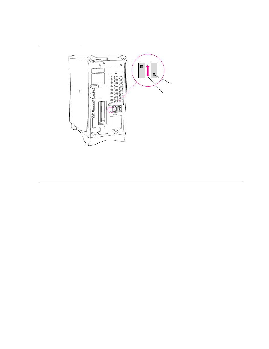
Power Supply
1
The power supply in the Power Macintosh 6500 tower enclosures is not self-configuring
for different input voltages. The voltage switch on tower enclosures is delivered
preconfigured for the input voltage of the region in which the unit is originally
purchased. If the computer is moved to another location where the input voltage is
different, a voltage switch must be adjusted to accommodate the voltage change.
The switch, shown in Figure 1-3, has two positions that support voltage ranges of 100 to
130 V or 220 to 270 V.
C H A P T E R 1
Introduction
Built-in Video and Graphics Features
13
Figure 1-3
Voltage switch on the tower enclosure
Built-in Video and Graphics Features
1
The logic board has the following built-in video and graphics capabilities:
■
ATI 3D RAGE II 64-bit graphics and multimedia accelerator (ATI264GT graphics
controller)
■
2 MB of synchronous graphic RAM (SGRAM)
■
hardware acceleration of 2D QuickDraw graphics and video to speed up scrolling text
and graphics and screen redraw operations
■
hardware acceleration of video for full screen, full motion, TV-quality playback of
Cinepak and MPEG1 QuickTime movies
■
bilinear hardware interpolation and scaling
■
accelerates 3D QuickDraw rendering up to 6 times that of software-only rendering
■
real-time 3D shaded object manipulation, animation, and virtual world navigation
■
includes 16-bit Z buffer for hidden texture surface removal
■
provides six perspectively correct texture-mapping functions
■
alpha blending, transparency, and fog effects
■
flat and Gouraud shading
■
video textures and video lighting
Set the switch to show “115” for
voltages in the 100–130V range.
Set the switch to show “230” for
voltages in the 200–270V range.
Check to see that the voltage
switch on the back of your
computer is properly set
before you plug it in. If you
need to change the setting,
insert a small screwdriver
here and slide the switch.

C H A P T E R 1
Introduction
14
QuickDraw 3D Acceleration and Video Memory
The graphics acceleration features enhance the realism of 3D interactive software titles
and games and also provide an affordable video authoring solution with the addition of
the optional Avid Cinema video input card.
For information about the supported display modes for video input and QuickDraw 2D
and QuickDraw 3D acceleration capabilities, see “Video Input and Graphics Acceleration
Display Modes” beginning on page 37.
QuickDraw 3D Acceleration and Video Memory
1
The logic board provides 2 MB of video memory for support of display modes up to 1152
by 870 at 16 bits of resolution. The largest supported display size is useful for standard
2D applications. For 3D applications, the 2 MB of video memory space is used
differently, which restricts the useful display size and supported bit depth. For example,
QuickDraw 3D utilizes double buffering if the hardware supports it. Double buffering
immediately reduces the available video memory for application use. In addition, 3D
applications that use a Z buffer for hidden texture removal have even less space
available for caching textures to increase graphics rendering speed.
To get the most performance out of 3D applications in the 2 MB of video memory, the
display mode size should be reduced. A 512-by-384 display mode is provided
specifically for increasing the available memory space for texture caching to improve 3D
graphics rendering speed.
Hardware acceleration for 3D applications is not provided for all of the supported 2D
display modes (see Table 3-11 on page 37 and Table 3-12 on page 38). For example, a
display mode of 640-by-480 at 32 bits set to use a front, back, and Z buffer for a 3D
application will not have sufficient memory space. Hardware acceleration is available for
the 640-by-480 display mode at 16 bits of resolution, however 3D application rendering
speeds are increased using the 512-by-384 display mode at 16 or 32-bit resolution. Game
applications using 3D acceleration can also adjust active window sizes to reduce the
video memory needed by the front, back, and Z buffers.
For more information about how the video memory is used, see Table 5-2 and Table 5-3
on page 76.

C H A P T E R 2
Architecture
2
Figure 2-0
Listing 2-0
Table 2-0

C H A P T E R 2
Architecture
16
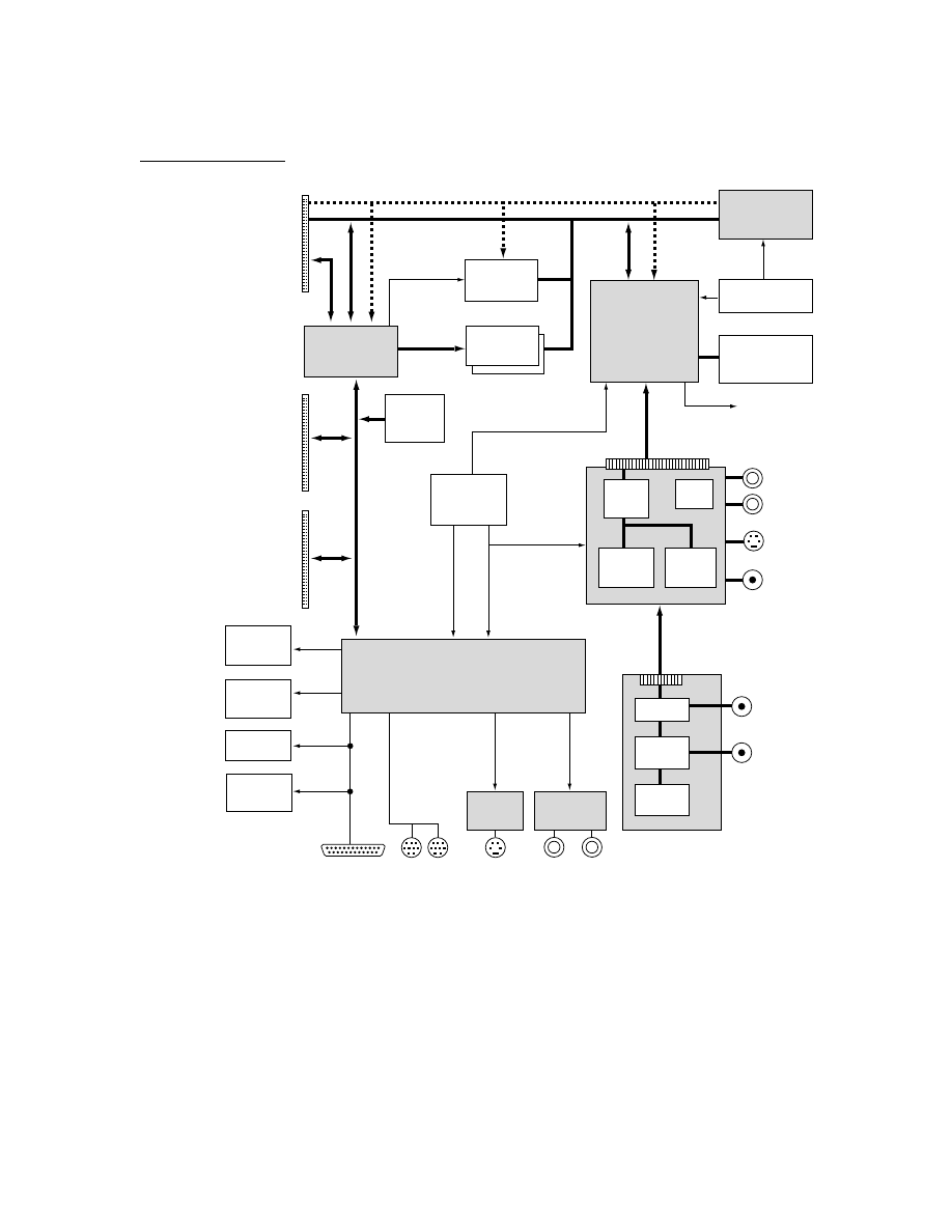
Block Diagram and Main ICs
This chapter describes the architecture of the Power Macintosh 5500 and 6500 main logic
board. It describes the major components of the main logic board: the microprocessor,
the custom ICs, and the display RAM. Input and output connectors are discussed in
Chapter 3, “I/O Features.”
Block Diagram and Main ICs
2
The architecture of the main logic board is designed to use the PowerPC 603e
microprocessor. Figure 2-1 shows the system block diagram. The architecture of the main
logic board is based on two buses: the processor bus and the PCI bus. The processor bus
connects the microprocessor, video, cache, and memory; the PCI bus connect the
expansion slots and the I/O devices.
PowerPC 603e Microprocessor
2
The main logic board uses a PowerPC 603e microprocessor running at 175 MHz,
200 MHz, 225 MHz, and 250 MHz. The principle features of the PowerPC 603e
microprocessor include
■
full RISC-processing architecture
■
parallel processing units: two integer and one floating-point
■
a branch manager that can usually implement branches by reloading the incoming
instruction queue without using any processing time
■
an internal memory management unit (MMU)
■
32 KB of on-chip cache memory (16 KB each for data and instructions)
For complete technical details, see the Motorola PowerPC 603 RISC Microprocessor User’s
Manual. This book is listed in “Supplemental Reference Documents,” in the preface.
Memory Subsystem
2
The memory subsystem of the main logic board consists of ROM and an optional
second-level (L2) cache, in addition to the internal cache memory of the PowerPC 603e
microprocessor. The PSX+ custom IC provides burst mode control to the cache and ROM.
ROM
2
The ROM consists of 4 MB of masked ROM soldered to the main logic board.
Second-Level Cache (Optional)
2
The optional second-level (L2) cache consists of 256 KB of high-speed RAM on a 160-pin
DIMM card, which is plugged into a 160-pin edge connector on the main logic board.
C H A P T E R 2
Architecture
Block Diagram and Main ICs
17
Figure 2-1
System block diagram
AWACS
Cuda
TEA
6330
Second-level
cache slot
PCI
slots
Communications
slot
ROM
4 MB
Internal
floppy
PCI
clocks
Hard
drive
CD-ROM
PSX+
ASIC
O'HareI/O controller
Address 32
Data 64
7140
scaler
DAV
slot
7110
decoder
RCA sound
jacks
RCA video
jack
SCSI
SCC
Sound ports
TV/FM tuner module
connects via
Foxconn cable
Sound
clock
37 MHz
37 MHz
SWIM
IDE
Video clock
Video-in board
plugs into video slot
RGB to monitor
Processor
clock
603e
PowerPC
Bus clock
2 MB video
SGRAM
ATI264GT
video/graphics
controller
QuickDraw
2D and 3D
accelerator
Clock
generator
PCI bus
ADB port
Serial ports
SCSI port
FM
Tuner
Stereo
decoder
F-connector
F-connector
TV tuner
Expansion
bay
S video
jack
2 DRAM
DIMMs

C H A P T E R 2
Architecture
18
Block Diagram and Main ICs
System RAM
2
The Power Macintosh 5500 and 6500 computers have 0 MB of DRAM memory soldered
on the main logic board. All RAM expansion is provided by DRAM devices on 8-byte
JEDEC-standard DIMMs (dual inline memory modules). Two 168-pin DIMM sockets are
used for memory expansion. Available DIMM sizes are 8, 16, 32, and 64 MB. The DIMM
sockets support both one- and two-bank DRAM modules. The PSX+ custom IC provides
memory control for the system RAM.
Custom ICs
2
The architecture of the main logic board is designed around five large custom integrated
circuits:
■
the PSX+ memory controller and PCI bridge
■
the O’Hare I/O subsystem and DMA engine
■
the AWACS sound processor
■
the Cuda ADB controller
■
the ATI264GT video/graphics controller
The computer also uses several standard ICs that are used in other Macintosh
computers. This section describes only the custom ICs.
PSX+ IC
2
The PSX+ IC functions as the bridge between the PowerPC 603e microprocessor and the
PCI bus. It provides buffering and address translation from one bus to the other.
The PSX+ IC also provides the control and timing signals for system cache, ROM, and
RAM. The memory control logic supports byte, word, longword, and burst accesses to
the system memory. If an access is not aligned to the appropriate address boundary,
PSX+ generates multiple data transfers on the bus.
Memory Control
2
The PSX+ IC controls the system RAM and ROM and provides address multiplexing and
refresh signals for the DRAM devices. For information about the address multiplexing,
see “RAM Address Multiplexing” on page 47.
PCI Bus Bridge
2
The PSX+ IC acts as a bridge between the processor bus and the PCI expansion bus,
converting signals on one bus to the equivalent signals on the other bus. The PCI bridge
functions are performed by two converters. One accepts requests from the processor bus
and presents them to the PCI bus. The other converter accepts requests from the PCI bus
and provides access to the RAM and ROM on the processor bus.

C H A P T E R 2
Architecture
Block Diagram and Main ICs
19
The PCI bus bridge in the PSX+ IC runs asynchronously so that the processor bus and
the PCI bus can operate at different rates. The processor bus operates at a clock rate of
50 MHz and the PCI bus operates at 33 MHz.
The PCI bus bridge generates PCI parity as required by the PCI bus specification, but it
does not check parity or respond to the parity error signal.
Big-Endian and Little-Endian Bus Addressing
2
Byte order for addressing on the processor bus is big-endian, and byte order on the PCI
bus is little-endian. The bus bridge performs the appropriate byte swapping and address
transformations to translate between the two addressing conventions. For more
information about the translations between big-endian and little-endian byte order, see
Part 1, “The PCI Bus,” in Designing PCI Cards and Drivers for Power Macintosh Computers.
Processor Bus to PCI Bus Transactions
2
Transactions from the processor bus to the PCI bus can be either burst or nonburst. Burst
transactions are always 32 bytes long and are aligned on cache-line or 8-byte boundaries.
In burst transactions, all the bytes are significant. Burst transactions are used by the
microprocessor to read and write large memory structures on PCI devices.
IMPORTANT
For the processor to generate PCI burst transactions, the address space
must be marked as cacheable. Refer to Macintosh Technote Number 1008,
Understanding PCI Bus Performance, for details.
▲
Nonburst transactions can be of arbitrary length from 1 to 8 bytes and can have any
alignment. Nonburst transactions are used by the processor to read and write small data
structures on PCI bus devices.
PCI Bus to Processor Bus Transactions
2
For transactions from the PCI bus to the processor bus, the bridge responds only to PCI
bus memory commands and configuration commands. On the processor bus, the bridge
generates a burst transaction or a nonburst transaction depending on the type of
command and the address alignment. For Memory Write and Invalidate commands that
are aligned with the cache line, the bridge generates a burst write transaction. Similarly,
for Memory Read Line and Memory Read Multiple commands whose alignment is less
than three-quarters through a cache line, the bridge generates a burst read transaction.
The maximum burst read or burst write transaction allowed by the bridge is 32 bytes—
eight PCI beats.
Commands other than those mentioned here are limited to two beats if aligned to a
processor bus doubleword boundary and to one beat otherwise.
O’Hare IC
2
The O’Hare IC is based on the Grand Central IC present in the Power Macintosh 7500
computer. It is an I/O controller and DMA engine for Power Macintosh computers using
the PCI bus architecture. It provides power-management control functions for energy

C H A P T E R 2
Architecture
20
Block Diagram and Main ICs
saving features included on Macintosh computers. The O’Hare IC is connected to the
PCI bus and uses the 33 MHz PCI bus clock.
The O’Hare IC includes circuitry equivalent to the IDE, SCC, SCSI, sound, SWIM3, and
VIA controller ICs. The functional blocks in the O’Hare IC include the following:
■
support for descriptor-based DMA for I/O devices
■
systemwide interrupt handling
■
a SWIM3 floppy drive controller
■
SCSI controller (MESH (Macintosh enhanced SCSI hardware) based)
■
SCC serial I/O controller
■
IDE hard disk interface controller
■
sound control logic and buffers
The O’Hare IC provides bus interfaces for the following I/O devices:
■
Cuda ADB controller IC (VIA1 and VIA2 registers)
■
AWACS sound input and output IC
■
8 KB nonvolatile RAM control
■
PWM outputs for brightness and contrast control
The SCSI controller in the O’Hare IC is a MESH controller. DMA channels in the O’Hare
IC are used to support data transfers. The clock signal to the SCSI controller is 45 MHz.
The O’Hare IC also contains the sound control logic and the sound input and output
buffers. There are two DMA data buffers—one for sound input and one for sound
output—so the computer can record sound input and process sound output
simultaneously. The data buffer contains interleaved right and left channel data for
support of stereo sound.
The SCC circuitry in the O’Hare IC is an 8-bit device. The PCLK signal to the SCC is an
16 MHz clock. The SCC circuitry supports GeoPort and LocalTalk protocols.
AWACS Sound IC
2
The audio waveform amplifier and converter (AWACS) is a custom IC that combines a
waveform amplifier with a 16-bit digital sound encoder and decoder (codec). It conforms
to the IT&T ASCO 2300 Audio-Stereo Codec Specification and furnishes high-quality sound
input and output. For information about the operation of the AWACS IC, see Chapter 3
of Developer Note: Power Macintosh Computers, available on the developer CD-ROM and
as part of Macintosh Developer Note Number 8.
Cuda IC
2
The Cuda IC is a custom version of the Motorola MC68HC05 microcontroller. It provides
several system functions, including
■
the ADB interface

C H A P T E R 2
Architecture
Block Diagram and Main ICs
21
■
management of system resets
■
management of the real-time clock
■
on/off control of the power supply (soft power)
■
the programming interface to devices on the IIC (interintegrated circuit) bus
The devices on the IIC bus include the AWACS sound IC, the digital video decoder and
scaler (DESC) on the video input module, and the Cyclops IC, which is the controller for
the remote control receiver. The computer reads and writes status and control
information to those devices by commands to the Cuda IC.
ATI264GT Graphics Controller
2
The ATI264GT graphics controller contains the logic for the video display. It includes the
following functions:
■
display memory controller, built-in drawing coprocessor, video scaler, color space
converter, clock generator, and true color palette video DAC (digital-to-analog
converter)
■
video CLUT (color lookup table)
■
hardware graphics acceleration with a 16-bit Z-buffer
■
accelerates QuickDraw 3D rendering up to 6 times that of software-only acceleration
■
true color palette DAC supporting pixel clock rates to 135 MHz for 1280 by 1024
resolution at 75 Hz
■
graphics and video line buffer for superior video scaling and playback quality
■
hardware cursor up to 64 x 64 x 2
■
DCC1 and DDC2B plug-and-play monitor support
■
supports synchronous graphics RAM (SGRAM) at up to 67 MHz memory clock,
providing a bandwidth up to 536 MB per second
■
Graphics control accessible through the QuickDraw , QuickDraw 3D, QuickDraw 3D
RAVE, and QuickTime components APIs
A separate data bus handles data transfers between the ATI264GT IC and the display
memory. The display memory data bus is 64 bits wide, and all data transfers consist of 32
bits at a time. The ATI264GT IC breaks each 64-bit data transfer into several pixels of the
appropriate size for the current display mode—4, 8, 16, 24, or 32 bits per pixel.
The ATI264GT IC uses several clocks. Its transactions are synchronized with the PCI bus.
Data transfers from the frame-buffer RAM are clocked by the MEM_CLK signal, which
runs at 67 MHz. Data transfers to the CLUT and the video output are clocked by the dot
clock, which has a different rate for different display monitors.
The 2D graphics accelerator is a fixed-function accelerator for rectangle fill, line draw,
polygon fill, panning/scrolling, bit masking, monochrome expansion, and scissoring.

C H A P T E R 2
Architecture
22
Block Diagram and Main ICs
For information about how application software can access the hardware acceleration
features of the ATI264GT graphics controller, see Chapter 5, “Software Components for
the 2D and 3D Hardware Graphics Accelerator.”
Display RAM
2
The display memory on the main logic board is separate from the main memory. The
display memory consists of 2 MB of 12-nanosecond (ns) SGRAM devices configured to
make a 64-bit data bus. The display memory cannot be expanded.
The display data generated by the computer can have pixel depths of 8, 16, or 32 bits for
monitors up to 832 by 624 pixels, 8 or 16 bits for larger monitors up to 1152 by 870 pixels,
and 8 bits for monitors supporting 1280 by 1024 pixels. Data from the video input
module is always stored and transferred at 16 bits per pixel. The video frame buffers
support live video in a 320-by-240 pixel frame at 30 frames per second.

C H A P T E R 3
I/O Features
3
Figure 3-0
Listing 3-0
Table 3-0
C H A P T E R 3
I/O Features
24
Serial I/O Ports
This chapter describes both the built-in I/O devices and the interfaces for external I/O
devices. It also describes the types of external video monitors that can be used with the
Power Macintosh 5500 and 6500 computers.
Serial I/O Ports
3
The main logic board has two built-in serial ports, one for a printer and one for a
modem. Both serial ports have 9-pin mini-DIN sockets that accept either 8-pin or 9-pin
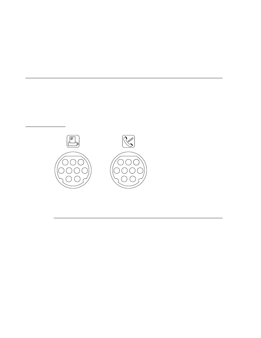
plugs. Both serial ports support the GeoPort serial protocol. Figure 3-1 shows the
mechanical arrangement of the pins on the serial port sockets; Table 3-1 shows the signal
assignments.
Figure 3-1
Serial port sockets
Table 3-1
Serial port signals
Pin
Name
Signal description
1
HSKo
Handshake output
2
HSKi
Handshake input (external clock on modem port)
3
TxD–
Transmit data –
4
Gnd
Ground
5
RxD–
Receive data –
6
TxD+
Transmit data +
7
GPi
General-purpose input (wakeup CPU or perform DMA handshake)
8
RxD+
Receive data +
9
+5V
+5 volts to external device (100 mA maximum)
Printer
Modem
8
7
1
5
4
2
3
9
6
8
7
1
5
4
2
3
9
6

C H A P T E R 3
I/O Features
ADB Port
25
Pin 9 on each serial connector provides +5 V power from the ADB power supply. An
external device should draw no more than 100 mA from that pin. The total current
available for all devices connected to the +5 V supply for the ADB and the serial ports is
500 mA. Excessive current drain will cause a fuse to interrupt the +5 V supply; the fuse
automatically resets when the load returns to normal.
Both serial ports include the GPi (general-purpose input) signal on pin 7. The GPi signal
for each port connects to the corresponding data carrier detect input on the SCC portion
of the O’Hare custom IC, described on page 19. On serial port A (the modem port), the
GPi line can be connected to the receive/transmit clock (RTxCA) signal on the SCC. That
connection supports devices that provide separate transmit and receive data clocks, such
as synchronous modems. For more information about the serial ports, see Guide to the
Macintosh Family Hardware, second edition.
The GeoPort serial hardware in conjunction with GeoPort software and a GeoPort
compatible telecom adapter provide access to a wide variety of telephony services. Some
examples are Fax send/receive, voice messaging, and hands-free phone. The logic board
provides a maximum of 300 mA of power for GeoPort from +5 volts at the serial
connector.
ADB Port
3
The Apple Desktop Bus (ADB) port on the logic board is functionally the same as on
other Macintosh computers.
The ADB is a single-master, multiple-slave serial communications bus that uses an
asynchronous protocol and connects keyboards, graphics tablets, mouse devices, and
other devices to the computer. The custom ADB microcontroller drives the bus and reads
status from the selected external device. A 4-pin mini-DIN connector connects the ADB
to the external devices. Table 3-2 lists the ADB connector pin assignments. For more
information about the ADB, see Guide to the Macintosh Family Hardware, second edition.
Table 3-2
ADB connector pin assignments
Pin number
Name
Description
1
ADB
Bidirectional data bus used for input and output. It is an
open-collector signal pulled up to +5 volts through a 470-ohm
resistor on the main logic board.
2
PSW
Power-on signal that generates reset and interrupt key
combinations.
3
+5V
+5 volts from the computer.
4
GND
Ground from the computer.

C H A P T E R 3
I/O Features
26
Disk Drives
Note
The total current available for all devices connected to the +5 V pins on
the ADB and the modem port is 500 mA. Each device should use no
more than 100 mA.
u
Disk Drives
3
The logic board support one internal high-density floppy disk drive, one internal ATA
(IDE) hard disk drive, and an internal SCSI CD-ROM drive. The Power Macintosh 6500
also provides an expansion bay for the addition of another SCSI device.
Floppy Disk Drive
3
The logic board suports one high-density floppy disk drive (Apple SuperDrive). The
drive is connected to a 20-pin connector on a cable that is connected to the main logic
board by the internal chassis connector. Table 3-3 shows the pin assignments on the
floppy disk connector.
Table 3-3
Pin assignments on the floppy disk connector
Pin number
Signal
name
Signal description
1
GND
Ground
2
PH0
Phase 0: state control line
3
GND
Ground
4
PH1
Phase 1: state control line
5
GND
Ground
6
PH2
Phase 2: state control line
7
GND
Ground
8
PH3
Phase 3: register write strobe
9
+5V
+5 volts
10
/WRREQ
Write data request
11
+5V
+5 volts
12
SEL
Head select
13
+12V
+12 volts
14
/ENBL
Drive enable
15
+12V
+12 volts
continued

C H A P T E R 3
I/O Features
Disk Drives
27
ATA (IDE) Hard Disk
3
The logic board supports an internal hard disk that uses the standard ATA-2 interface.
This interface, used for ATA drives on IBM AT–compatible computers, is also referred to
as the IDE interface. The implementation of the ATA interface on the logic board is a
subset of the ATA interface specification, ANSI proposal X3T9.2/90-143, Revision 3.1.
Hard Disk Specifications
3
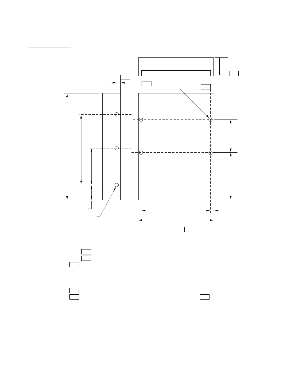
Figure 3-2 shows the maximum dimensions of the hard disk and the location of the
mounting holes. As the figure shows, the minimum clearance between conductive
components and the bottom of the mounting envelope is 0.5 mm.
16
RD
Read data
17
+12V
+12 volts
18
WR
Write data
19
+12V
+12 volts
20
n.c.
Not connected
Table 3-3
Pin assignments on the floppy disk connector (continued)
C H A P T E R 3
I/O Features
28
Disk Drives
Figure 3-2
Maximum dimensions of the hard disk
6.40 (.252)2x
3
IDE connector
Power
Mounting hole 6-32, .22"
min. full thread, 4X
A
B
A
7
101.6 (4.00)
95.25 (3.75)
3.20 (.125) 2
60.30 (2.37)
44.40 (1.75)
60.00 (2.36) 2x
101.6 (4.00) 2x
146.0 (5.75)
25.4 (1.00)
16.00 (.63) 2x
Mounting hole
6-32, through 6x
Notes:
1
2
3
4
5
6
7
8
A Defined by plane of bottom mount holes
B Defined by center line of bottom mount holes
40-pin IDE and 4-pin power connector placement must not be reversed
Dimensions are in millimeters (inches)
Drawing not to scale
Tolerances .X = +
0.50, .XX = +
0.25
Dimension to be measured at center line of side-mount holes
Minimum 0.5 MM clearance from any conductive PCB components to A
–
–

C H A P T E R 3
I/O Features
Disk Drives
29
Hard Disk Connectors
3
The internal hard disk has a standard 40-pin ATA connector and a separate 4-pin power
connector. The 40-pin connector cable is part of the cable harness attached to the main
logic board by the internal chassis connector. The power cable is attached directly to the
power supply.
The exact locations of the ATA connector and the power connector are not specified, but
the relative positions must be as shown in Figure 3-2 so that the cables and connectors
will fit.
Pin Assignments
3
Table 3-4 shows the pin assignments on the 40-pin ATA (IDE) hard disk connector. A
slash (/) at the beginning of a signal name indicates an active-low signal.
Table 3-4
Pin assignments on the ATA (IDE) hard disk connector
Odd-numbered
pins
Signal name
Even-numbered
pins
Signal name
1
/RESET
2
GROUND
3
DD7
4
DD8
5
DD6
6
DD9
7
DD5
8
DD10
9
DD4
10
DD11
11
DD3
12
DD12
13
DD2
14
DD13
15
DD1
16
DD14
17
DD0
18
DD15
19
GROUND
20
Key
21
Reserved
22
GROUND
23
DIOW
24
GROUND
25
DIOR
26
GROUND
27
/IORDY
28
Reserved
29
Reserved
30
GROUND
31
INTRQ
32
/IOCS16
33
DA1
34
/PDIAG
35
DA0
36
DA2
37
/CS0
38
/CS1
39
/DASP
40
GROUND

C H A P T E R 3
I/O Features
30
Disk Drives
ATA (IDE) Signal Descriptions
3
Table 3-5 describes the signals on the ATA (IDE) hard disk connector.
CD-ROM Drive
3
The Power Macintosh 5500 and 6500 computers have a 12X-speed internal CD-ROM
drive. The CD-ROM drive supports the worldwide standards and specifications for
CD-ROM and CD-digital audio discs described in the Sony/Philips Yellow Book and
Red Book. The drive can read CD-ROM, CD-ROM XA, CD-I, and PhotoCD discs as well
as play standard audio discs.
Table 3-5
Signals on the ATA (IDE) hard disk connector
Signal name
Signal description
DA(0–2)
ATA device address; used by the computer to select one of the registers
in the ATA drive. For more information, see the descriptions of the CS0
and CS1 signals.
DD(0–15)
ATA data bus; buffered from IOD(16–31) of the computer’s I/O bus.
DD(0–15) are used to transfer 16-bit data to and from the drive buffer.
DD(8–15) are used to transfer data to and from the internal registers of
the drive, with DD(0–7) driven high when writing.
/CS0
ATA register select signal. It is asserted high to select the additional
control and status registers on the ATA drive.
/CS1
ATA register select signal. It is asserted high to select the main task file
registers. The task file registers indicate the command, the sector
address, and the sector count.
/IORDY
ATA I/O ready; when driven low by the drive, signals the CPU to insert
wait states into the I/O read or write cycles.
/IOCS16
ATA I/O channel select; asserted low for an access to the data port. The
computer uses this signal to indicate a 16-bit data transfer.
DIOR
ATA I/O data read strobe.
DIOW
ATA I/O data write strobe.
INTRQ
ATA interrupt request. This active high signal is used to inform the
computer that a data transfer is requested or that a command has
terminated.
/RESET
Hardware reset to the drive; an active-low signal.
Key
This pin is the key for the connector.

C H A P T E R 3
I/O Features
SCSI Bus
31
The CD-ROM drive has a sliding tray to hold the disc. The drive features a mechanism
that supports 4X, 8X, and 12X data transfer rates and a data buffer that further enhances
performance. Table 3-6 is a summary of the specifications of the CD-ROM drive.
SCSI Bus
3
The logic board has a SCSI bus for the internal CD-ROM device, one additional internal
SCSI device, and one or more external SCSI devices. The CD-ROM device and any
additional internal SCSI device receive power directly from the power supply.
SCSI Connectors
3
The SCSI connector for the internal SCSI devices is a 50-pin connector with the standard
SCSI pin assignments. It attaches to a cable that is connected to the main logic board by
the internal chassis connector. The external SCSI connector is a 25-pin D-type connector
with the same pin assignments as other Apple SCSI devices. Table 3-7 shows the pin
assignments on the internal and external SCSI connectors.
Table 3-6
Specifications of the CD-ROM drive
Feature
Specification
Rotation speed
Approximately 230 to 4240 rpm
Average access time
Less than 200 ms
Sustained transfer rate
1800 KB per second
SCSI burst rate
Asynchronous 5 MB per second,
synchronous 10 MB per second
Table 3-7
Pin assignments for the SCSI connectors
Pin number
(internal 50-pin)
Pin number
(external 25-pin)
Signal name
Signal description
2
8
/DB0
Bit 0 of SCSI data bus
4
21
/DB1
Bit 1 of SCSI data bus
6
22
/DB2
Bit 2 of SCSI data bus
8
10
/DB3
Bit 3 of SCSI data bus
10
23
/DB4
Bit 4 of SCSI data bus
12
11
/DB5
Bit 5 of SCSI data bus
continued

C H A P T E R 3
I/O Features
32
Sound
SCSI Bus Termination
3
The internal end of the SCSI bus is terminated by an active terminator. The terminator is
located on the main logic board near the O’Hare ASIC. On enclosures with only one
internal SCSI device located close to the logic board, the active termination is
automatically enabled. On enclosures with multiple SCSI devices, the active termination
is disabled and a positive terminator is located at the end of the internal bus.
Sound
3
The sound system supports 16-bit stereo sound output and input, available
simultaneously. SRS (sound retrieval system) enhanced sound output can be optionally
turned on and off through the Sound panel of the Monitors & Sound control panel. No
additional software API is available for controlling the SRS sound enhancement.
Like other Macintosh logic boards, the Power Macintosh 5500 and 6500 logic board and
system software can create sounds digitally and either play the sounds through speakers
14
12
/DB6
Bit 6 of SCSI data bus
16
13
/DB7
Bit 7 of SCSI data bus
18
20
/DBP
Parity bit of SCSI data bus
25
–
n.c. Not
connected
26
25
TPWR
+5 V terminator power
32
17
/ATN
Attention
36
6
/BSY
Bus busy
38
5
/ACK
Handshake acknowledge
40
4
/RST
Bus reset
42
2
/MSG
Message phase
44
19
/SEL
Select
46
15
/C/D
Control or data
48
1
/REQ
Handshake request
50
3
/I/O
Input or output
20, 22, 24, 28,
30, 34, and all
odd pins
except pin 25
7, 9, 14, 16, 18,
and 24
GND
Ground
Table 3-7
Pin assignments for the SCSI connectors (continued)
Pin number
(internal 50-pin)
Pin number
(external 25-pin)
Signal name
Signal description

C H A P T E R 3
I/O Features
Sound
33
inside the enclosure or send the sound signals out through the sound output jacks. The
logic board also records sound from several sources: an internal microphone on
all-in-one enclosures, a microphone connected to the sound input jack, the sound in on
the video input module, the sound from the optional TV/FM Radio tuner module,
analog sound from optional communication cards connected to the comm slot II, a
compact disc in the CD-ROM player, or analog sound from a cross-platform card in a
PCI slot. With each sound input source, sound playthrough can be enabled or disabled.
Sound Output
3
The Power Macintosh 6500 tower enclosure has one built-in speaker/subwoofer and two
sound output jacks, one on the front and one on the back. Both output jacks are
connected to the sound amplifier; the jack on the front is intended for ease of access
when connected to a pair of headphones. Inserting a plug into the front jack disconnects
the internal speakers. The rear jack is intended for use with external speakers, and it is
muted when headphones are plugged into the front jack. When the rear jack is used for
external speakers, the subwoofer mode in the tower enclosure is enabled. (Options in the
Monitors & Sound control panel can be used to determine the interaction between the
sound input and output devices.) The Power Macintosh 5500 all-in-one enclosure has a
pair of front-facing stereo speakers and sound output jacks at the front and rear. In the
all-in-one enclosure, the internal speakers are turned off when the rear jack is used for
external speakers.
Sound output is controlled by the O’Hare IC. The AWACS IC provides the stereo sound
output to both the internal speakers and the sound output jacks.
Sound Input
3
The all-in-one and tower enclosures have a stereo sound input jack on the back for
connecting an external microphone or other sound source. The sound input jack accepts
a standard 1/8-inch stereophonic phone plug (two signals plus ground).
The sound input jack accepts either the Apple PlainTalk line-level microphone or a pair
of line-level signals.
Note
The Apple PlainTalk microphone requires power from the main
computer, which it obtains by way of an extra-long, 4-conductor plug
that makes contact with a 5-volt pin inside the sound input jack.
◆
IMPORTANT
The microphone for the Macintosh LC and LC II does not work with the
Power Macintosh 5500 and 6500 computers; it requires the line-level
signal provided by the Apple PlainTalk microphone.
▲
Sound from an external source, such as a TV, VCR, or VTR, can also be input through the
right and left channel sound input jacks on the optional video-in module.

C H A P T E R 3
I/O Features
34
Keyboard
Sound Input Specifications
3
The sound input jack has the following electrical characteristics:
■
input impedance: 10 k
Ω
■
maximum input level: 2 V peak to peak (Vpp) maximum
Routing of the Sound Signals
3
All audio sources are routed to the AWACS custom IC. The AWACS IC can enable the
input sources in two groups: the sound input jack (external microphone) or (CD-ROM,
TV/FM Radio tuner, modem, DAV card, cross-platform card).
Digitizing Sound
3
The logic board digitizes and records sound as 16-bit samples. The computer can use any
one of three sampling rates: 11.025K samples per second, 22.050K samples per second, or
44.01K samples per second.
The sound system plays samples at the sampling rate specified in the Monitors and
Sound control panel for sound.
Sound Modes
3
The sound mode is selected by a call to the Sound Manager. The sound circuitry
normally operates in one of three modes:
■
Sound playback: computer-generated sound is sent to the speaker and the sound
output jacks.
■
Sound playback with playthrough: computer sound and sound input are mixed and
sent to the speakers and the sound output jacks.
■
Sound record with playthrough: input sound is recorded and also sent to the speakers
and the sound output jacks.
When recording from a microphone, applications should reduce the playthrough volume
to prevent possible feedback from the speakers to the microphone.
The O’Hare IC provides separate sound buffers for input and for stereo output so that
the computer can record and send digitized sound to the sound outputs simultaneously.
Keyboard
3
The keyboard has a Power key, identified by the symbol
p
. When the user chooses Shut
Down from the Special menu, the computer either shuts down or a dialog box appears
asking if you really want to shut down. The user can also turn off the power by pressing
the Power key.

C H A P T E R 3
I/O Features
Built-in Video
35
There are no programmer’s switches, so the user invokes the reset and nonmaskable
interrupt (NMI) function by pressing Command-key combinations while holding down
the Power key, as shown in Table 3-8. The Command key is identified by the symbols
ð
and
x
.
Note
The user must hold down a key combination for at least 1 second to
allow the ADB microcontroller enough time to respond to the NMI or
hard-reset signal.
◆
Note
The NMI function can always be activated from the keyboard. This is a
change from the Macintosh LC computer, where keyboard activation of
the NMI function can be disabled by the software.
◆
Built-in Video
3
On tower enclosures the built-in video circuitry supports pixel display sizes of
512 by 384, 640 by 480, 800 by 600, 832 by 624, 1024 by 768, 1152 by 870, 1280 by 960, and
1280 by 1024. On all-in-one enclosures the video cirtuitry supports pixel display sizes of
512 by 384, 640 by 480, 800 by 600, 832 by 624, and 1024 by 768. When power is applied,
the monitor is initially set for a display size of 640 by 480 pixels. The user can switch the
monitor resolution on the fly from the Monitor BitDepth and Monitor Resolution
modules in the Control Strip or from the Monitors & Sound control panel.
For more information about the built-in video capabilities of the all-in-one enclosure, see
the Power Macintosh 5400 Developer Note.
External Video Connection for Tower Enclosures
3
The Power Macintosh 6500 tower enclosure requires an external monitor. The cable from
the external monitor plugs into a DB-15 video port located on the upper-left part of the
enclosure’s rear panel. Power Macintosh 5500 ll-in-one enclosures have a built-in
Table 3-8
Reset and NMI key combinations
Key combination
Function
Command-Power (
x
-
p
)
NMI (always active)
Control-Command-Power (Control-
x
-
p
)
Reset

C H A P T E R 3
I/O Features
36
Built-in Video
monitor and an optional external video display mirror output connector. The pin
assignments for the external video connector on the logic board are shown in Table 3-9.
External Video Monitors
3
The logic board can drive several sizes of external video monitors. Table 3-10 shows the
monitor types, display resolution, horizontal refresh, vertical refresh, pixel clock, and
maximum pixel depth supported by the display graphics subsystem.
Table 3-9
Pin assignments for the external video connector
Pin number
Signal name
Description
1
RED.GND
Red video ground
2
RED.VID
Red video signal
3
/CSYNC
Composite synchronization signal
4
SENSE0
Monitor sense signal 0
5
GRN.VID
Green video signal
6
GRN.GND
Green video ground
7
SENSE1
Monitor sense signal 1
9
BLU.VID
Blue video signal
10
SENSE2
Monitor sense signal 2
11
GND
CSYNC and VSYNC ground
12
/VSYNC
Vertical synchronization signal
13
BLU.GND
Blue video ground
14
HSYNC.GND
HSYNC ground
15
/HSYNC
Horizontal synchronization signal
Shell
SGND
Shield ground
Table 3-10
Maximum pixel depths for video monitors
Monitor type
Display
resolution
Horizontal
refresh rate
Vertical
refresh rate
Pixel clock
Maximum
pixel depth
12-inch RGB
512 by 384
24.48 kHz
60.147 Hz
15.667 MHz
32
VGA
640 by 480
31.469 kHz
59.94 Hz
25.175 MHz
32
13-inch RGB
640 by 480
35.00 kHz
66.667 Hz
30.24 MHz
32
VESA
640 by 480
43.269 kHz
85.008 Hz
36.00 MHz
32
continued

C H A P T E R 3
I/O Features
Built-in Video
37
Video Input and Graphics Acceleration Display Modes
3
Table 3-11 shows the display modes that the tower enclosure supports for video input
and QuickDraw 2D and QuickDraw 3D acceleration.
15-inch RGB
(full page)
640 by 870
68.85 kHz
75.00 Hz
57.283 MHz
16
VESA
800 by 600
37.879 kHz
60.317 Hz
40.00 MHz
32
VESA
800 by 600
48.077 kHz
72.188 Hz
50.00 MHz
32
VESA
800 by 600
46.875 kHz
75.00 Hz
49.50 MHz
32
VESA
800 by 600
53.674 kHz
85.061 Hz
56.25 MHz
32
16-inch RGB
832 by 624
49.725 kHz
74.550 Hz
57.283 MHz
32
VESA
1024 by 768
48.363 kHz
60.004 Hz
65.00 MHz
16
VESA
1024 by 768
56.476 kHz
70.069 Hz
75.00 MHz
16
VESA
1024 by 768
60.023 kHz
75.029 Hz
78.750 MHz
16
19-inch RGB
1024 by 768
60.241 kHz
74.927 Hz
80.00 MHz
16
VESA
1024 by 768
68.677 kHz
84.997 Hz
94.50 MHz
16
21-inch RGB
1152 by 870
68.681 kHz
75.062 Hz
100 MHz
16
VESA
1280 by 1024
63.981 kHz
60.020 Hz
108 MHz
8
VESA
1280 by 1024
79.976 kHz
75.025 Hz
135 MHz
8
Table 3-11
Tower enclosure video input and graphics acceleration display modes
Display
resolution
Pixel
depth
Vertical scan rate
Video
input
QuickDraw 2D
acceleration
QuickDraw 3D
acceleration
512 by 384
8
70 Hz
Yes
Yes
No
512 by 384
16, 32
70 Hz
Yes
Yes
Yes
640 by 480
8
60 Hz, 67 Hz, 72 Hz,
75 Hz, 85 Hz
Yes
Yes
No
640 by 480
16
60 Hz, 67 Hz, 72 Hz,
75 Hz, 85 Hz
Yes
Yes
Yes
640 by 480
32
60 Hz, 67 Hz, 72 Hz,
75 Hz, 85 Hz
Yes
Yes
Depends on
application
window size
continued
Table 3-10
Maximum pixel depths for video monitors
Monitor type
Display
resolution
Horizontal
refresh rate
Vertical
refresh rate
Pixel clock
Maximum
pixel depth

C H A P T E R 3
I/O Features
38
Built-in Video
Table 3-12 shows the display modes that the all-in-one enclosure supports for video
input and QuickDraw 2D and QuickDraw 3D acceleration.
640 by 870
16
75 Hz
Yes
Yes
No
800 by 600
8, 32
56 Hz, 60 Hz, 72 Hz,
75 Hz, 85 Hz
Yes
Yes
No
800 by 600
16
56 Hz, 60 Hz, 72 Hz,
75 Hz, 85 Hz
Yes
Yes
Depends on
application
window size
832 by 624
8, 32
75 Hz
Yes
Yes
No
832 by 624
16
75 Hz
Yes
Yes
Depends on
application
window size
1024 by 768
8, 16
60 Hz, 70 Hz, 75 Hz
Yes
Yes
No
1152 by 870
16
75 Hz
Yes
Yes
No
1280 by 980
8
75 Hz
Yes
Yes
No
1280 by 1024
8
60 Hz, 75 Hz
Yes
Yes
No
Table 3-12
All-in-one enclosure video input and graphics acceleration display modes
Display
resolution
Pixel
depth
Vertical scan rate
Video
input
QuickDraw 2D
acceleration
QuickDraw 3D
acceleration
640 by 480
8
60 Hz, 67 Hz
Yes
Yes
No
640 by 480
16
60 Hz, 67 Hz
Yes
Yes
Yes
640 by 480
32
60 Hz, 67 Hz
Yes
Yes
Depends on
application
window size
800 by 600
8, 32
60 Hz, 72 Hz
Yes
Yes
No
800 by 600
16
60 Hz, 72 Hz
Yes
Yes
Depends on
application
window size
832 by 624
8, 32
75 Hz
Yes
Yes
No
832 by 624
16
75 Hz
No
Yes
Depends on
application
window size
1024 by 768
8, 16
60 Hz
Yes
Yes
No
Table 3-11
Tower enclosure video input and graphics acceleration display modes (continued)
Display
resolution
Pixel
depth
Vertical scan rate
Video
input
QuickDraw 2D
acceleration
QuickDraw 3D
acceleration

C H A P T E R 3
I/O Features
GIMO Edge-Connector Socket
39
GIMO Edge-Connector Socket
3
The GIMO (graphics internal monitor out) is a 16-pin edge-connector socket. The
primary function for the GIMO socket is to provide an interface for the Apple 7-inch PC
compatibility card to the main logic board. The GIMO interface is the best way to
integrate the PC compatibility card with the Macintosh host system, since the PC video
can be alternately driven onto the built-in monitor port or the external monitor port on
the PC compatibility card without using an additional loop-back cable. See the 12” and
7” PC Compatibility Cards Developer Note for more information about the GIMO interface.

40

C H A P T E R 4
Expansion Features
4
Figure 4-0
Listing 4-0
Table 4-0

C H A P T E R 4
Expansion Features
42
RAM DIMMs
This chapter describes the expansion features of the Power Macintosh 5500 and 6500
logic board: the RAM expansion slot, the L2 cache expansion slot, the PCI expansion slot,
the DAV connector on the video input module, the communications slot, and the
expansion bay for SCSI devices.
The expansion features of the logic board are like those of the Power Macintosh 5400 and
Macintosh Performa 6400 computers. Therefore, much of the information in this chapter
is the same as that found in the developer notes that support the Macintosh 5400 and
Performa 6400 computers. The primary difference between the Power Macintosh 5500
and 6500 logic board expansion features and the expansion features of the logic board in
the Macintosh 5400 and Performa 6400 is the speed of the memory bus, which is 50 MHz
rather than 40 MHz and full support for EDO DRAM devices. Memory and L2 cache
should be screened to support the higher clock speed of the memory bus on the logic
board.
Note
Apple does not support development of third-party cards for the video
input slot, nor does Apple support development of third-party
second-level (L2) cache cards.
◆
RAM DIMMs
4
The Power Macintosh 5500 and 6500 logic board has two RAM expansion slots. The
RAM expansion slots accept the 8-byte DIMM (dual inline memory module). As its name
implies, the 8-byte DIMM has a 64-bit-wide data bus. The DIMM slot accommodates
168-pin 5-volt fast-paged and EDO DRAM DIMMs.
The mechanical design of the DRAM DIMM is defined by the MO-161 specification
published by the JEDEC JC-11 committee; its electrical characteristics are defined by the
JEDEC Standard No. 21-C. The DRAM DIMM connector used is Burndy Corporation’s
part number ELF168E5GC-3Z50 or equivalent.
The minimum bank size supported by the PSX+ IC is 4 MB, and the largest is 32 MB; the
largest DIMM supported is a two-bank DIMM holding 64 MB. Table 4-1 shows the
single-bank DIMM configurations and sizes for a range of DRAM device sizes that are
supported on the logic board.
Table 4-1
Memory sizes and configurations for single bank DIMMS
Device size
DIMM configuration
DIMM size
Maximum memory with
2 DIMMs installed
4 Mbit
512K by 64
4 MB
8 MB
4 Mbit
1 Mbit by 64
8 MB
16 MB
continued

C H A P T E R 4
Expansion Features
RAM DIMMs
43
Note
It is possible to use 5-volt fast-paged mode or EDO (extended data out)
memory devices in the DIMM slots; EDO DIMMs must have the
presence detect 5 (PD5) pin open or not connected. If the EDO DIMM
has PD5 high and is mixed with a fast-paged mode DIMM, the logic
board may not operate at fast-paged mode timings. The 3.3-volt EDO
DIMM cards are not supported and will not mechanically fit into the
DIMM connectors on the logic board.
◆
The DRAM DIMMs can be installed one or more at a time. The logic board supports only
linear memory organization; therefore no performance gains are seen when two DIMMs
of the same size are installed. Any supported size DIMM can be installed in either DIMM
slot, and the combined memory of all of the DIMMs installed will be configured as a
contiguous array of memory.
RAM DIMM Connectors
4
Table 4-2 gives the pin assignments for the RAM DIMM connectors.
16 Mbit
1 Mbit by 64
8 MB
16 MB
16 Mbit
2 Mbits by 64
16 MB
32 MB
16 Mbit
4 Mbits by 64
32 MB
64 MB
Table 4-2
Pin assignments on the RAM DIMM connectors
Pin number
Signal name
Pin number
Signal name
1
VSS
85
VSS
2
DQ(0)
86
DQ(32)
3
DQ(1)
87
DQ(33)
4
DQ(2)
88
DQ(34)
5
DQ(3)
89
DQ(35)
6
VCC
90
VCC
7
DQ(4)
91
DQ(36)
8
DQ(5)
92
DQ(37)
9
DQ(6)
93
DQ(38)
10
DQ(7)
94
DQ(39)
continued
Table 4-1
Memory sizes and configurations for single bank DIMMS (continued)
Device size
DIMM configuration
DIMM size
Maximum memory with
2 DIMMs installed

C H A P T E R 4
Expansion Features
44
RAM DIMMs
11
Reserved
95
Reserved
12
VSS
96
VSS
13
DQ(8)
97
DQ(40)
14
DQ(9)
98
DQ(41)
15
DQ(10)
99
DQ(42)
16
DQ(11)
100
DQ(43)
17
DQ(12)
101
DQ(44)
18
VCC
102
VCC
19
DQ(13)
103
DQ(45)
20
DQ(14)
104
DQ(46)
21
DQ(15)
105
DQ(47)
22
Reserved
106
Reserved
23
VSS
107
VSS
24
Reserved
108
Reserved
25
Reserved
109
Reserved
26
VCC
110
VCC
27
/WE(0)
111
Reserved
28
/CAS(0)
112
/CAS(1)
29
/CAS(2)
113
/CAS(3)
30
/RAS(0)
114
/RAS(1)
31
/OE(0)
115
Reserved
32
VSS
116
VSS
33
A(0)
117
A(1)
34
A(2)
118
A(3)
35
A(4)
119
A(5)
36
A(6)
120
A(7)
37
A(8)
121
A(9)
38
A(10)
122
A(11)
39
Not connected
123
Not connected
40
VCC
124
VCC
41
Reserved
125
Reserved
continued
Table 4-2
Pin assignments on the RAM DIMM connectors (continued)
Pin number
Signal name
Pin number
Signal name

C H A P T E R 4
Expansion Features
RAM DIMMs
45
42
Reserved
126
B(0)
43
VSS
127
VSS
44
/OE(2)
128
Reserved
45
/RAS(2)
129
/RAS(3)
46
/CAS(4)
130
/CAS(5)
47
/CAS(6)
131
/CAS(7)
48
/WE(2)
132
/PDE
49
VCC
133
VCC
50
Reserved
134
Reserved
51
Reserved
135
Reserved
52
DQ(16)
136
DQ(48)
53
DQ(17)
137
DQ(49)
54
VSS
138
VSS
55
DQ(18)
139
DQ(50)
56
DQ(19)
140
DQ(51)
57
DQ(20)
141
DQ(52)
58
DQ(21)
142
DQ(53)
59
VCC
143
VCC
60
DQ(22)
144
DQ(54)
61
Reserved
145
Reserved
62
Reserved
146
Reserved
63
Reserved
147
Reserved
64
Reserved
148
Reserved
65
DQ(23)
149
DQ(55)
66
Reserved
150
Reserved
67
DQ(24)
151
DQ(56)
68
VSS
152
VSS
69
DQ(25)
153
DQ(57)
70
DQ(26)
154
DQ(58)
71
DQ(27)
155
DQ(59)
72
DQ(28)
156
DQ(60)
continued
Table 4-2
Pin assignments on the RAM DIMM connectors (continued)
Pin number
Signal name
Pin number
Signal name

C H A P T E R 4
Expansion Features
46
RAM DIMMs
Table 4-3 describes the signals on the RAM DIMM connector.
73
VCC
157
VCC
74
DQ(29)
158
DQ(61)
75
DQ(30)
159
DQ(62)
76
DQ(31)
160
DQ(63)
77
Reserved
161
Reserved
78
VSS
162
VSS
79
PD(1)
163
PD(2)
80
PD(3)
164
PD(4)
81
PD(5)
165
PD(6)
82
PD(7)
166
PD(8)
83
ID(0)
167
ID(1)
84
VCC
168
VCC
Table 4-3
RAM DIMM signals
Signal name
Description
A(0–11)
Address inputs
/CAS(0–7)
Column address strobe signals
DQ(0–63)
Data input and output signals
ID(0–1)
Memory module identification (not used)
/OE(0, 2)
Output enable signals
PD(1–8)
Presence detect signals
/PDE
Presence detect enable signal (not used)
/RAS(0-3)
Row address strobe signals
Reserved
Reserved; don’t use
VCC
+5 V power
VSS
Ground
/WE(0, 2)
Read/write input signals
Table 4-2
Pin assignments on the RAM DIMM connectors (continued)
Pin number
Signal name
Pin number
Signal name

C H A P T E R 4
Expansion Features
RAM DIMMs
47
RAM Address Multiplexing
4
Signals A[0–11] on each RAM DIMM make up a 12-bit multiplexed address bus that can
support several different types of DRAM devices. Table 4-4 shows the address
multiplexing modes used with several types of DRAM devices. The devices are
characterized by their bit dimensions: for example, a 256K by 4-bit device has 256K
addresses and stores 4 bits at a time.
Table shows how the address signals to the RAM devices are multiplexed during the row
and column address phases for noninterleaved banks.
IMPORTANT
The PSX+ DRAM controller does not provide support for 2 M by 8 bits
with 12 by 9 addressing, or 1 M by 16 bits with 11 by 9 addressing, or
1 M by 4 bits with 11 by 9 addressing DRAM devices.
▲
Table 4-4
Address multiplexing modes for various DRAM devices
Device size
Device type
Size of row
address
Size of column
address
4 Mbits
512K by 8 bits
10
9
4 Mbits
1 M by 4 bits
10
10
16 Mbits
1 M by 16 bits
10
10
16 Mbits
2 M by 8 bits
11
10
16 Mbits
4 M by 1 bits
11
11
16 Mbits
4 M by 4 bits
11
11
16 Mbits
4 M by 1 bits
12
10
16 Mbits
4 M by 4 bits
12
10
64 Mbits
4 M by 16 bits
12
10
Table 4-5
Address multiplexing in noninterleaved banks
Individual signals on the DRAM_ADDR bus
A(11)
A(10)
A(9)
A(8)
A(7)
A(6)
A(5)
A(4)
A(3)
A(2)
A(1)
A(0)
Row address
22
23
21
20
19
18
17
16
15
14
13
12
Column address
24
22
11
10
9
8
7
6
5
4
3

C H A P T E R 4
Expansion Features
48
RAM DIMMs
RAM Devices
4
The memory controller in the PSX+ IC supports 1 MB, 4 MB, and 16 MB DRAM devices.
The access time (T
RAS
) of the DRAM devices is 60 ns or faster.
Note
The computer supplies +5 volts at VCC on the RAM expansion slot for
DRAM DIMMs. Power for DRAM devices that require 3.3 volts is not
supplied on the RAM expansion slot.
◆
RAM Refresh
4
The PSX IC provides a CAS-before-RAS refresh cycle every 15.6
µ
s. DRAM devices must
be compatible with this refresh cycle; for example, this cycle will refresh 2K-refresh parts
within 32 milliseconds.
RAM DIMM Dimensions
4
Figure 4-1 shows the dimensions of the RAM DIMM.
IMPORTANT
The JEDEC MO-161 specification shows three possible heights for the
DRAM DIMM. For Power Macintosh computers, developers should use
only the shortest of the three: 1.100 inches. Taller DIMMs put excessive
pressure on the DIMM sockets due to possible mechanical interference
inside the case.
▲
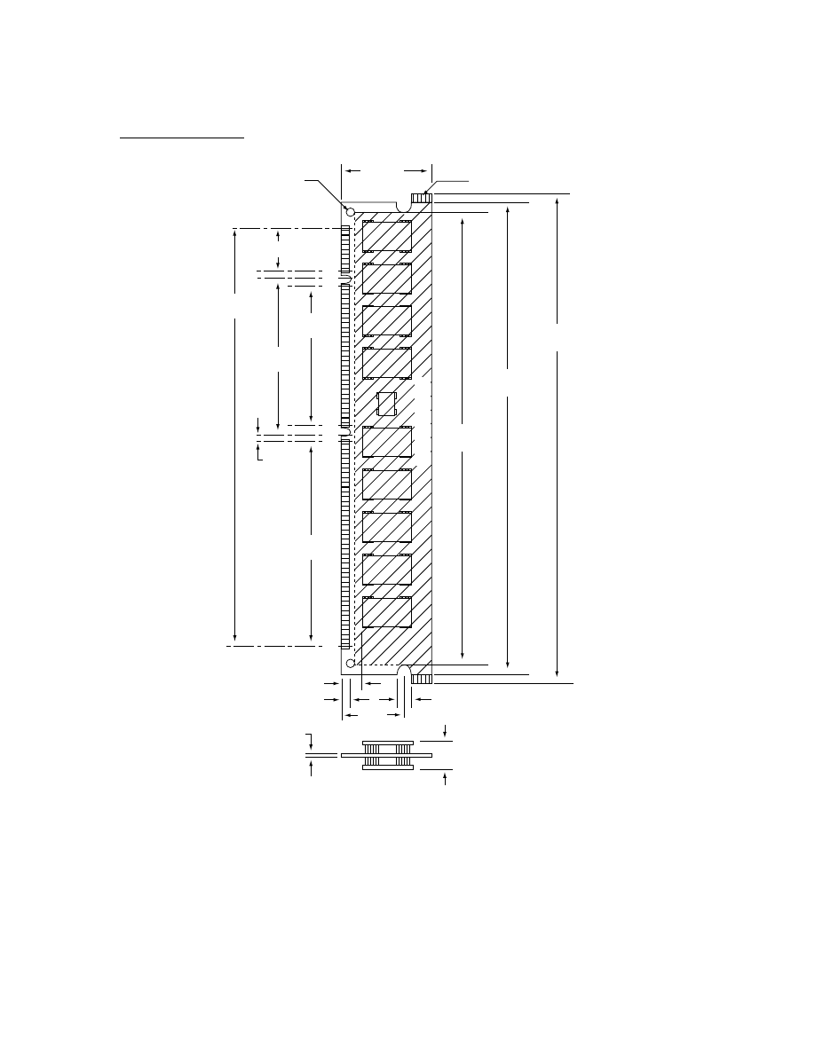
C H A P T E R 4
Expansion Features
RAM DIMMs
49
Figure 4-1
Dimensions of the RAM DIMM
+
40
41
10
11
84
+
+
Optional tabs
Optional holes
2XO 3.00
±
0.10
(0.118
±
0.004)
138.32–138.58
(5.445–5.456)
133.22–133.48
(5.245–5.255)
Component area
127.35
(5.01)
11.43 (0.450)
3.175
(0.125)
36.83
(1.450)
54.61
(2.150)
4.00 (0.157) minimum
4.00
±
0.10
(0.157
±
0.004)
Note: dimensions are in millimeters (inches)
9.40 (0.370) maximum
1.27
±
0.10
(0.50
±
0.004)
3.00 (0.118)
17.78
(0.700)
43.18
(1.700)
115.57
(4.550)
27.94
(1.1)
maximum
/

C H A P T E R 4
Expansion Features
50
Second-Level Cache DIMM
Second-Level Cache DIMM
4
The main logic board has a slot for a second-level (L2) cache on a DIMM.
The L2 cache DIMM contains the cache controller, tag, and data store memory. It is a
lookaside cache, which is connected to the PowerPC 50 MHz processor bus. Several
signals are also included to control cache operation. These signals include: /L2_DIS,
/MEM_INHIBIT, /L2_BR, /L2_BG, and L2_PRSNT.
Table 4-6 shows the pin and signal assignments on the L2 cache DIMM connector.
Table 4-6
Pin and signal assignments for L2 cache DIMM connector
Pin
Signal name
Pin
Signal name
Pin
Signal name
Pin
Signal name
1
+5 V
41
A15
81
D63 (LSB)
121
A16
2
D31
42
A13
82
D62
122
A14
3
D30
43
+3.3 V
83
D61
123
A12
4
D29
44
A11
84
GND
124
A10
5
D28
45
A9
85
D60
125
A8
6
D27
46
A7
86
D59
126
GND
7
+5 V
47
A5
87
D58
127
A6
8
D26
48
A3
88
D57
128
A4
9
D25
49
+3.3 V
89
D56
129
A2
10
D24
50
A1
90
GND
130
A0 (MSB)
11
D23
51
/WT
91
D55
131
/DBB
12
D22
52
/GBL
92
D54
132
GND
13
+5 V
53
reserved
93
D53
133
/CPU_BG
14
D21
54
/SRESET
94
D52
134
/CPU_BR
15
D20
55
+3.3 V
95
D51
135
L2_PRSNT
16
D19
56
TTYPE0
96
GND
136
reserved
17
D18
57
TTYP1
97
D50
137
TSIZ0
18
D17
58
TTYPE2
98
D49
138
GND
19
+5 V
59
TTYPE3
99
D48
139
TSIZ1
20
D16
60
TTYPE4
100
/L2_DIS
140
TSIZ2
21
/L2_BR
61
+3.3 V
101
/TBST
141
SHD
continued

C H A P T E R 4
Expansion Features
Second-Level Cache DIMM
51
Table 4-7 defines the signals on the L2 cache DIMM connector.
22
/L2_BG
62
D15
102
GND
142
D47
23
TC0
63
D14
103
/CI
143
D46
24
TC1
64
D13
104
/RSRV
144
GND
25
+3.3 V
65
D12
105
reserved
145
D45
26
/HRESET
66
D11
106
/MEM_INHIBIT
146
D44
27
/TEA
67
+5 V
107
/AACK
147
D43
28
/TS
68
D10
108
GND
148
D42
29
GND
69
D9
109
/TA
149
D41
30
SYS_CLK
70
D8
110
/ARTRY
150
GND
31
+3.3 V
71
D7
111
/ABB
151
D40
32
A31 (LSB)
72
D6
112
A30
152
D39
33
A29
73
+5 V
113
A28
153
D38
34
A27
74
D5
114
GND
154
D37
35
A25
75
D4
115
A26
155
D36
36
A23
76
D3
116
A24
156
GND
37
+3.3 V
77
D2
117
A22
157
D35
38
A21
78
D1
118
A20
158
D34
39
A19
79
+5 V
119
A18
159
D33
40
A17
80
D0 (MSB)
120
GND
160
D32
Table 4-7
Signal descriptions for L2 cache DIMM connector
Signal name
Description
+5 V
Power supply voltage of +5 volts for tag RAM (5% tolerance)
+ 3.3 V
Power supply voltage of +3.3 volts for data RAM (5% tolerance)
GND
Ground
A(0-31)
Processor address bus signals 0 through 31
D(0-63)
Processor data bus signals 0 through 63; sampled on the rising edge
of the CLK signal during a write cycle
/AACK
Address acknowledge, same as AACK_ signal on PowerPC 603
continued
Table 4-6
Pin and signal assignments for L2 cache DIMM connector (continued)
Pin
Signal name
Pin
Signal name
Pin
Signal name
Pin
Signal name

C H A P T E R 4
Expansion Features
52
Second-Level Cache DIMM
/ARTRY
Address retry, same as ARTRY_ signal on PowerPC 603
/ABB
Address bus busy, same as ABB_ signal on PowerPC 603
/CI
Cache inhibit, same as CI_ signal on PowerPC 603
/CPU_BG
Bus transaction granted, same as BG_ signal on PowerPC 603
/CPU_BR
Bus transaction requested, same as BR_ signal on PowerPC 603
/DBB
Data bus busy, same as DBB_ signal on PowerPC 603
/GBL
Global transaction
/HRESET
Main logic board hardware reset
/L2_BG
Bus grant to L2 cache; used only in copyback mode
/L2_BR
Bus request from L2 cache; used only in copyback mode
/L2_DIS
Disables cache when low; contents are invalidated
L2_PRSNT
L2 cache present; tied directly to power rail on cache DIMM
/MEM_INHIBIT
Indicates L2 cache will source the data for the current cycle.
Inhibits main logic board memory controller.
/RSRV
Reservation signal, same as RSRV_ signal on PowerPC 603
reserved
DO NOT USE
SHD
Share
/SRESET
Soft reset, same as SRESET_ signal on PowerPC 603
SYS_CLK
System clock, same as SYSCLOCK signal on PowerPC 603
/TA
Transfer acknowledge, same as TA_ signal on PowerPC 603
/TBST
Transfer burst in progress, same as TBST_ signal on
PowerPC 603
TC(0-1)
Transfer code, same as TC signal on PowerPC 603
/TEA
Transfer error acknowledge, same as TEA_ signal on PowerPC 603
/TS
Transfer start signal, same as TS_ signal on PowerPC 603
TSIZ (0-2)
Transfer size for the data transaction
TTYPE(0-4)
Transfer type, same as TT signal on PowerPC 603
/WT
Write-through, same as WT_ signal on PowerPC 603
Table 4-7
Signal descriptions for L2 cache DIMM connector (continued)
Signal name
Description

C H A P T E R 4
Expansion Features
PCI Expansion Slot
53
PCI Expansion Slot
4
The main logic board uses the industry-standard peripheral component interconnect
(PCI) bus for an I/O expansion bus. The PCI bus is a 32-bit multiplexed address and
data bus. The PCI expansion slot has a 33.33 MHz system clock.
PCI I/O expansion cards are mounted horizontally in a 90-degree straight-through
adapter board, which is installed in the PCI expansion slot on the main logic board.
A total of 15 watts of power is provided for each of the PCI expansion slots. Both 5 volts
and 3.3 volts are supplied; the total power consumed by both voltages must not exceed
the 15-watt maximum.
The main logic board requires that PCI cards use the 5-volts signaling standard
described in the PCI Local Bus Specification, Revision 2.0.
The enclosures allow for standard 6.88-inch PCI cards as defined by the PCI Local Bus
Specification, Revision 2.0. The cards are required to use the standard ISA fence described
in the specification.
The PCI slots support all the required PCI signals and certain optional PCI signals. The
supported PCI signals are listed in Table 4-3.
Table 4-8
PCI signals
Signal name
Description
AD [0–31]
Address and data, multiplexed
C/BE[0–3]
Bus command and byte enable signals, multiplexed
PAR
Parity; used with AD and C/BE signals
FRAME#
Cycle frame; asserted to indicate a bus transaction
TRDY#
Target ready; selected device is able to complete the current phase
IRDY#
Initiator ready; master device is able to complete the current phase
STOP#
Stop; indicates the current target device is requesting the master to stop
the current transaction
DEVSEL#
Device select; indicates that the driving device has decoded its address
as the target of the current access
IDSEL
Initialization device select; used during configuration
REQ#
Request; indicates to the arbiter that the asserting agent requires use of
the bus
GNT#
Grant; indicates to the agent that access to the bus has been granted
CLK
Clock; rising edge provides timing for all transactions
continued

C H A P T E R 4
Expansion Features
54
The DAV Connector
The PCI slots on the main logic board do not support the optional 64-bit bus extension
signals or cache support signals.
For more information about the PCI expansion slot, refer to Designing PCI Cards and
Drivers for Power Macintosh Computers.
The DAV Connector
4
The optional video input card has a separate connector called the DAV (digital audio
video) connector. The DAV connector provides access to the video input card’s 4:2:2
unscaled YUV video input data bus and associated control signals. By means of a 60-pin
cable to the DAV connector, a PCI expansion card can gain access to the digital video bus
on the video input card and use it to transfer real-time video data to the computer. Such
a PCI expansion card can contain a hardware video compressor or other video processor.
The DAV connector accepts YUV video and analog sound from the expansion card but
does not itself generate YUV video output or audio output signals.
The DAV connector is a 60-pin flat-ribbon connector located at the top edge of the video
input card. PCI expansion card are connected to the video in card with a 7-inch
60-conductor flat-ribbon cable that the user can install between the DAV connector and
the PCI card. The DAV connecting cable is shown in Figure 4-2, where dimensions are
given in millimeters with inch equivalents in brackets.
RST#
Reset; used to bring registers and signals to a known state
INTA#,
INTB#,
INTC#,
INTD#
Interrupt request pins; wired together on each slot
LOCK#
Lock; indicates an operation that may require multiple transactions to
complete.
PERR#
Parity error; used to report data parity errors during PCI transactions
excluding a Special Cycle transaction.
SERR#
System error; used to report address parity errors, data parity errors
during a Special Cycle, or any other system error that will be
catastrophic.
Table 4-8
PCI signals (continued)
Signal name
Description
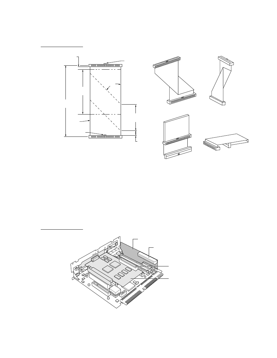
C H A P T E R 4
Expansion Features
The DAV Connector
55
Figure 4-2
DAV connecting cable
Cable fold option A, shown in Figure 4-2, is used for tower and minitower models such
as the Macintosh Performa 6400 and Power Macintosh 8500; fold option B is used in
all-in-one models such as the Power Macintosh 5400 and low-profile models such as the
Performa 6360. Total cable length in both cases is 7 inches.
Figure 4-3 is a view of the main logic board showing the PCI expansion card and the
location of the DAV connector on the video input card.
Figure 4-3
Location of the DAV connector
45
°
6.3
[0.25]
108.7
[4.28]
177.8
[7.00]
63.8
[2.51]
10.0
[0.39]
Fold option A
Fold option B
Note: Dimensions are in millimeters [inches].
B
B
PIN 1
(red stripe)
Key
Key
A
A
Video input card
DAV connector
DAV connector
PCI card with DAV
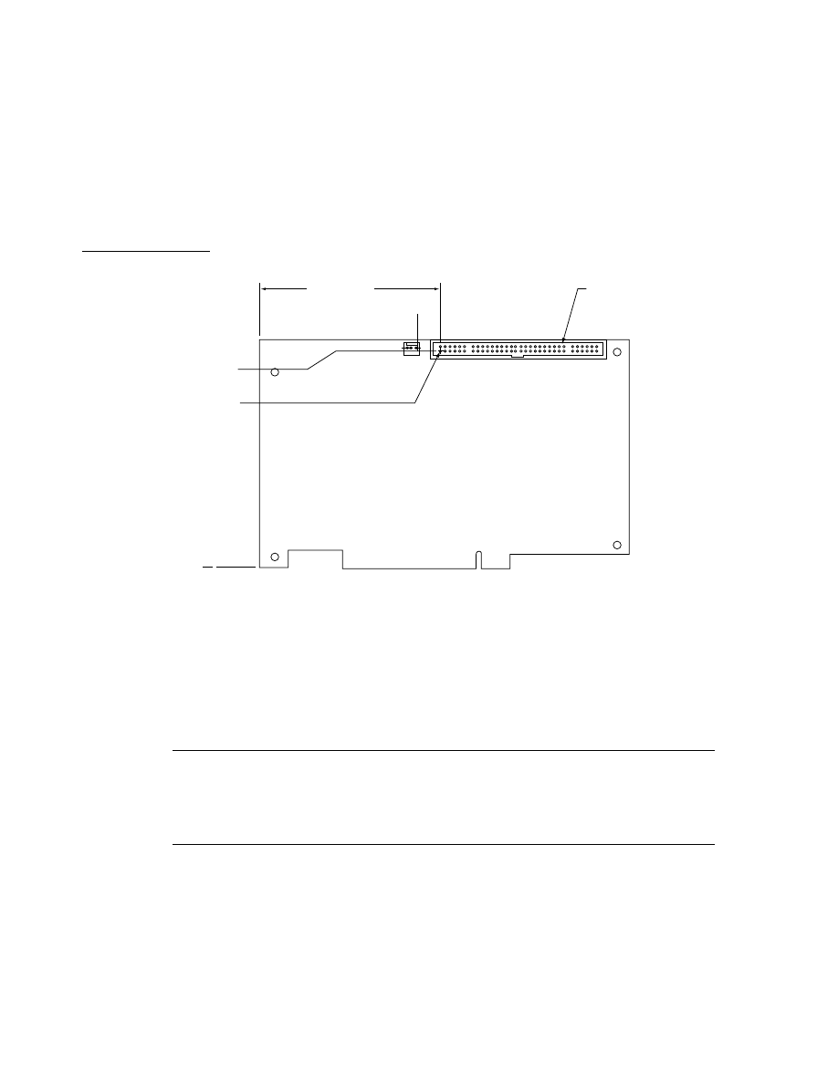
C H A P T E R 4
Expansion Features
56
The DAV Connector
The interface of the 60-pin DAV connector is a superset of the interface on the 34-pin
DVA connector found on PDS slot video-in cards for the Power Macintosh 5200, Power
Macintosh 6200, and Macintosh Quadra 630 computers.
Figure 4-4 shows the orientation of the DAV connector on the video input module.
Figure 4-4
Orientation of the DAV connector
The DAV connector on the video input card provides some of the functionality of the
DAV connectors found on the Power Macintosh Power Macintosh 7100 and 8100 models,
and the Macintosh Quadra
AV
models, but it is not compatible with any of those
connectors. Refer to Macintosh DAV Interface for NuBus Expansion Cards in Developer Note
Number 8 for more information.
Pin Assignments
4
The DAV connector on the video-in card is a 60-pin dual-row type with 0.100-inch pin
spacing. The pin assignments on the DAV connector are shown in Table 4-9.
Table 4-9
Pin assignments on the DAV connector
Odd-numbered
pins
Signal name
Even-numbered
pins
Signal name
1
Ground
2
GEOPORT_CLK
3
Ground
4
LLC_OUT
continued
96.33 [3.793]
(pin 1)
60-pin DAV connector
Pin 1
77.39 [3.047]
(pin 1)
0

C H A P T E R 4
Expansion Features
The DAV Connector
57
5
Ground
6
PXQ_OUT
7
Ground
8
VS_OUT
9
Ground
10
HS_OUT
11
UV bit 7
12
UV bit 6
13
UV bit 5
14
UV bit 4
15
UV bit 3
16
UV bit 2
17
UV bit 1
18
UV bit 0
19
Y bit 7
20
Y bit 6
21
Y bit 5
22
Y bit 4
23
Y bit 3
24
Y bit 2
25
Y bit 1
26
Y bit 0
27
Ground
28
LLC_IN
29
Ground
30
PXQ_IN
31
Ground
32
VS_IN
33
Ground
34
HS_IN
35
Ground
36
HREF_IN
37
Ground
38
FLD
39
IIC_DATA
40
IIC_CLK
41
Ground
42
SND_L
43
SND_RET
44
SND_R
45
Ground
46
AUDIO_SDIN
47
Ground
48
AUDIO_SDOUT
49
Ground
50
AUDIO_BITCLK
51
Ground
52
AUDIO_SYNC
53
Ground
54
NC
55
VID_RET
56
NC
57
VID_RET
58
NC
59
NC
60
NC
Table 4-9
Pin assignments on the DAV connector (continued)
Odd-numbered
pins
Signal name
Even-numbered
pins
Signal name

C H A P T E R 4
Expansion Features
58
The DAV Connector
Table 4-10 gives descriptions of the signals on the DAV connector.
Signal Levels
4
When designing PCI card hardware to support the DAV connection, observe these rules:
■
Connect a 47
Ω
resistor in series between the bidirectional signals of the DAV
connector and any PCI expansion card circuitry that drives output or bidirectional
signals. This rule applies to pins 11 through 26, 28, 30, 32, and 36.
■
Do not make any electrical connections to pins 2, 4, 6, 8, 10, 34, and 58 through 60.
These pins are marked Reserved in Table 4-9.
Table 4-11 lists the required signal levels for the digital input and output pins in the DAV
interface.
Table 4-10
Descriptions of the signals on the DAV connector
Signal name
Signal description
LLC_OUT
Clock reference signal
FLD
YUV directional signal
HS_IN
Horizontal reference signal
HS_OUT
Horizontal sync signal
LLC_IN
Line-locked clock signal
UV(bits 0–7)
Digital chrominance data bus
VS_OUT
Vertical sync signal
Y(bits 0–7)
Digital luminance data bus
Table 4-11
DAV signal levels
Specification
Minimum
Maximum
Input voltage low
–0.3 V
0.8 V
Input voltage high
2.4 V
Input current drain
±
20
µ
A
Output voltage low
0.4 V
Output voltage high
3.5 V
Output current
±
400
µ
A
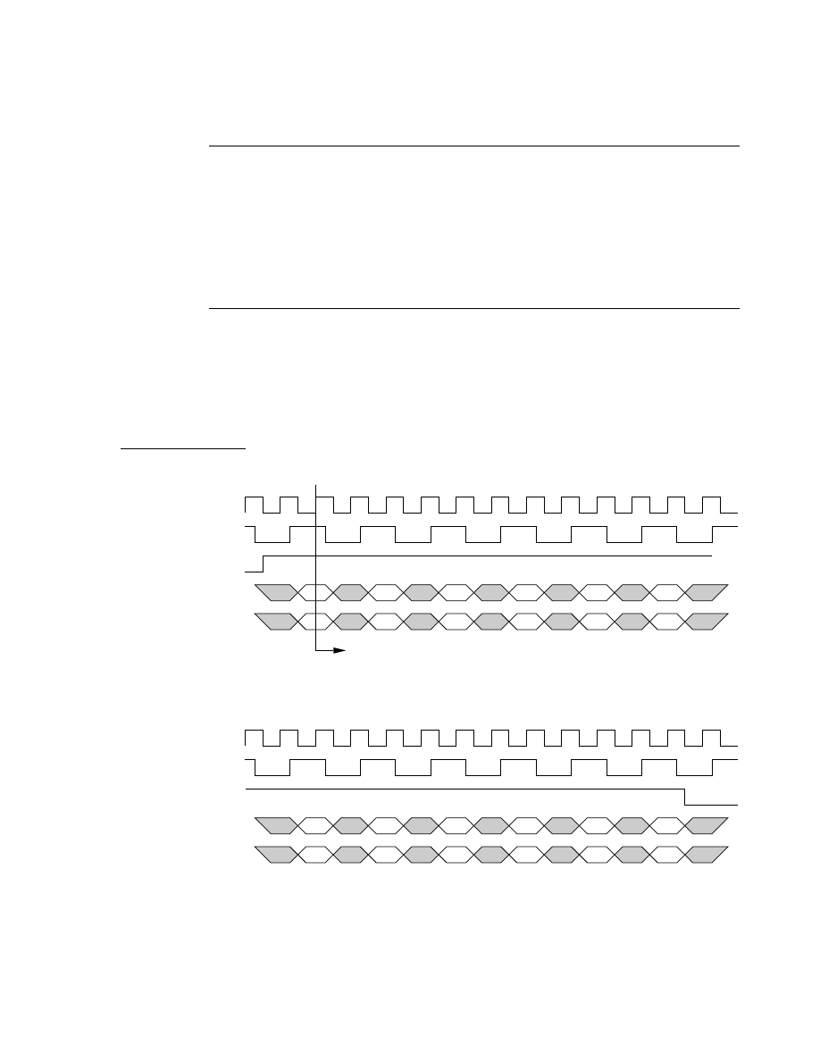
C H A P T E R 4
Expansion Features
The DAV Connector
59
Using the YUV Bus
4
The video input module contains a digital video decoder and scaler (DESC), the Philips
SAA7140 IC. Logic on the video input card uses the CVBS port on the DESC and pulls
the FLD signal low, disabling the YUV bus. For an expansion card to use the YUV bus,
the software associated with the card must set the FLD signal high so that the DESC will
accept data on the YUV bus. For information about using the registers in the DESC IC,
please refer to the SAA7140 Philips Desktop Video Handbook.
Video Data Format
4
Digital video data is transmitted as lines and fields. Each line consists of an even number
of samples on the Y and UV buses as shown in Figure 4-5. HREF is high during a video
line and low during the horizontal blanking interval. The falling edge of the VS signal
indicates the beginning of a video field. For more information about digital video data in
YUV format, see the Power Macintosh DAV Interface for PCI Expansion Cards.
Figure 4-5
Video data timing
Y 0
LLCLK
vdcCREFB
HREF
Y 7–0
UV 7–0
Start of a video line
Y1
Y2
Y3
Y4
Y5
U 0
V0
U2
V2
U4
V4
Y and UV data valid on the rising edge of LLCLK
when HREF and CREFB are high
Yn-5
LLCLK
vdcCREFB
HREF
Y 7–0
UV 7–0
End of a video line
Yn-4
Yn-3
Yn-2
Yn-1
Yn
Un-5
Vn-5
Un-3
Vn-3
Un-1
Vn-1

C H A P T E R 4
Expansion Features
60
The PCI Bus Communications Slot
The PCI Bus Communications Slot
4
The main logic board has a separate slot for an optional communications card. The
communications slot on the main logic board is a PCI bus–based communications slot
(comm slot II) rather than a processor direct PDS–based communications slot (comm
slot I) like that found on the Power Macintosh 5200 and 6200 computers.
The electrical interface of the communications slot is a parallel bus, the SCC lines, and
lines for supporting modem audio. The PSX+ custom IC provides bus conversion from
the host PowerPC 603e bus to the PCI parallel bus. Cards that use the communications
slot are memory mapped into the I/O space of the main logic board via the parallel bus.
The communications slot supports SCC port A (modem port) for installing a universal
modem card that is compatible with both the communications slot in the Power
Macintosh 5200 and 6200 computers and the PCI bus communications slot.
PCI Bus Communications Slot Connector
4
The PCI bus communications slot connector is a 112-pin half-height microchannel
connector. A communications card mounts vertically in the connector and its I/O
connector is accessed through the communications port access hole on the right hand
side of the back panel. The size constraints of a communications card are 1.57 inches (40
mm) wide by 6 inches (152 mm) long.
A maximum of 2.5 watts of power is allocated to the communications slot. The
maximum possible current ratings for each power line are
Voltage
Current
+5 V
500 mA
+12 V
100 mA
Trickle +5 V
5 mA
–5 V
20 mA
Table 4-12 lists the pin assignments of the PCI bus communications slot.
Table 4-12
Pin assignments for the PCI bus communications slot connector
Odd-numbered pins
Function
Even-numbered pins
Function
1
/DCD
2
/DTR
3
/CTS
4
/RTS
5
RxD
6
TxD
7
IN_SENSE
8
SCC_ENAB
9
INT_MIC
10
MIC_SENSE

C H A P T E R 4
Expansion Features
The PCI Bus Communications Slot
61
11
MIC_RET
12
EXT_AUD_L
13
Reserved
14
EXT_AUD_RET
15
GND
16
+12V
17
-5V
18
+12V
19
SYS_WAKEUP
20
Trickle +5
21
GND
22
GND
23
A1
24
A0
25
A3
26
A2
27
+3.3V
28
+3.3V
29
A5
30
A4
31
A7
32
A6
33
+5V
34
+5V
35
A8
36
C/BE(0)~
37
A10
38
A9
39
GND
40
GND
41
A12
42
A11
43
A14
44
A13
45
C/BE(1)~
46
A15
47
GND
48
Gnd
49
SERR~
50
PAR
51
PERR~
52
SBO~
53
LOCK~
54
SDONE
55
+3.3V
56
+3.3V
57
DEVSEL~
58
STOP~
59
IRDY~
60
TRDY~
61
+5V
62
+5V
63
C/BE(2)~
64
FRAME~
65
A17
66
A16
67
GND
68
GND
69
A19
70
A18
71
A21
72
A20
continued
Table 4-12
Pin assignments for the PCI bus communications slot connector (continued)
Odd-numbered pins
Function
Even-numbered pins
Function

C H A P T E R 4
Expansion Features
62
The PCI Bus Communications Slot
Universal Serial Modem Card
4
The PCI bus communications slot (comm slot II) on the main logic board is not
compatible with cards designed only for the PDS communications slot (comm slot I) in
the Power Macintosh 5200 and 6200 computers. As shown in Figure 4-6, such cards will
not physically fit into the communications slot on the logic board, because the
communications slot is keyed at the opposite end.
73
A23
74
A22
75
GND
76
GND
77
C/BE(3)~
78
IDSEL
79
A25
80
A24
81
A27
82
A26
83
+3.3V
84
+3.3V
85
A29
86
A28
87
A31
88
A30
89
+5V
90
+5V
91
REQ~
92
GNT~
93
+5V
94
+5V
95
INT~
96
Reserved
97
Reserved
98
RST~
99
GND
100
Reserved‘
101
CLK
102
Reserved
103
GND
104
Reserved
105
Reserved
106
Reserved
107
Reserved
108
Reserved
109
CommGnd
110
RefGnd
111
AudToSlot
112
AudFromSlot
Table 4-12
Pin assignments for the PCI bus communications slot connector (continued)
Odd-numbered pins
Function
Even-numbered pins
Function
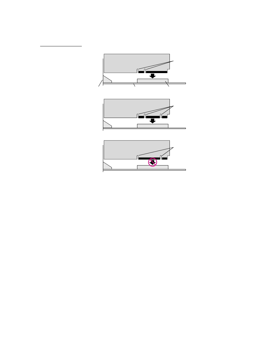
C H A P T E R 4
Expansion Features
The PCI Bus Communications Slot
63
Figure 4-6
Communications slot card compatibility
However, the signals on comm slot II are configured to make it possible to design a
universal communications slot card that works in both commm slots if access to the
parallel bus is not required (for example, a serial modem card). The power, ground,
serial, and audio signals of comm slot II on the main logic board are located on the
connector in such a way that a dual-keyed (notched) modem card will fit and operate in
the Power Macintosh 5200, 6200 and 5400, LC 575, LC 630, Macintosh Peforma 6400 and
Power Macintosh 5500 and 6500 logic board. A simplified design diagram for a
dual-keyed universal modem card is shown in Figure 4-7.
Vertical plate
Compatible
Compatible
Notches
Logic board
(side view)
Communication slot
Communication card
Notches
Not compatible
Notches
C H A P T E R 4
Expansion Features
64
The PCI Bus Communications Slot
Figure 4-7
Universal modem card for communications slot
IMPORTANT
Serial modem cards designed for universal operation must not attempt
to access the parallel bus of either the 68030-bus or the PCI-bus
communications slots to be compatible in both configurations.
▲
Table 4-13 lists the pin assignments on a universal serial modem card that operates in the
68030-bus or PCI-bus communications slots. The assignments are the same as those on
the PCI bus communications slot, listed in Table 4-12, with the PCI bus signals removed
and the addition of the key slot location.
Table 4-13
Pin assignments for a universal serial modem card
Odd-numbered pins
Function
Even-numbered pins
Function
1
/DCD
2
/DTR
3
/CTS
4
/RTS
5
RxD
6
TxD
7
IN_SENSE
8
SCC_ENAB
9
INT_MIC
10
MIC_SENSE
11
MIC_RET
12
EXT_AUD_L
13
Not connected
14
EXT_AUD_RET
Pin number 1 location
odd pins on this side
Edge connector
Pin number 1 location
even pins on this side
RJ11
Secondary side
restricted component height,
see official drawing
Primary or
component side
6.0622
inches
1.8898
inches

C H A P T E R 4
Expansion Features
The PCI Bus Communications Slot
65
15
Gnd
16
+12V
17
–5V
18
Not connected
19
SYS_WAKEUP
20
Trickle+5
21
GND
22
Not connected
key (pin 23)
key slot (cutout)
key (pin 24)
key slot (cutout)
key (pin 25)
key slot (cutout)
key (pin 26)
key slot (cutout)
27
Not connected
28
Not connected
29
Not connected
30
Not connected
31
Not connected
32
Not connected
33
Not connected
34
+5V
35
Not connected
36
Not connected
37
Not connected
38
Not connected
39
Not connected
40
Not connected
41
Not connected
42
Not connected
43
Not connected
44
Not connected
45
Not connected
46
Not connected
47
GND
48
Not connected
49
Not connected
50
Not connected
51
Not connected
52
Not connected
53
Not connected
54
Not connected
55
Not connected
56
Not connected
57
Not connected
58
Not connected
59
Not connected
60
Not connected
61
Not connected
62
+5V
63
Not connected
64
Not connected
65
Not connected
66
Not connected
67
Not connected
68
Not connected
69
Not connected
70
Not connected
71
Not connected
72
Not connected
73
Not connected
74
Not connected
75
GND
76
Not connected
continued
Table 4-13
Pin assignments for a universal serial modem card (continued)
Odd-numbered pins
Function
Even-numbered pins
Function

C H A P T E R 4
Expansion Features
66
Expansion Bay for SCSI Devices
Expansion Bay for SCSI Devices
4
The expansion bay in the tower enclosure supports the addition of 3.5 and 5.25-inch SCSI
devices. The electrical and mechanical guidelines for utilizing the expansion bay are
defined in this section.
Mechanical Specifications
4
The expansion bay, shown in Figure 4-8, is located at the top of the tower enclosure. It
accommodates a wide range of SCSI devices with a maximum width of 5.25-inch (152.0
mm), a maximum height of 1.72 inches (43.6 mm), and a maximum length of 8.268 inches
(210.0 mm).
77
Not connected
78
Not connected
79
Not connected
80
Not connected
81
Not connected
82
Not connected
83
Not connected
84
Not connected
85
Not connected
86
Not connected
87
Not connected
88
Not connected
89
Not connected
90
+5V
key
key slot (cutout)
key
key slot (cutout)
key
key slot (cutout)
key
key slot (cutout)
91
Not connected
92
Not connected
93
Not connected
94
Not connected
95
Not connected
96
Reserved
97
Reserved
98
RST~
99
GND
100
Reserved
101
Not connected
102
Not connected
103
GND
104
Reserved
105
Reserved
106
Reserved
107
Reserved
108
Reserved
109
CommGnd
110
RefGnd
111
AudFromSlot
112
AudToSlot
Table 4-13
Pin assignments for a universal serial modem card (continued)
Odd-numbered pins
Function
Even-numbered pins
Function
C H A P T E R 4
Expansion Features
Expansion Bay for SCSI Devices
67
Figure 4-8
Tower enclosure expansion bay
Drive Carrier
4
The expansion bay enclosure incorporates a carrier guide mounting mechanism that is
designed to work with the drive carrier (Apple part number 815-2501). The drive carrier
is attached to the bottom of the SCSI device. To attach the carrier to the device, the
mounting holes in the plastic carrier may have to be modified to align with the mounting
holes on the SCSI device. The SCSI device with carrier slides into the enclosure and
snaps into place on the carrier guide.
Expansion Bay Cover
4
The plastic expansion bay cover (Apple part number 815-2344, manufactured by Li Xin
Plastic Industries, AppleLink LI.XIN) and attached EMI shield (Apple part number
805-1393, available from Allied Technologies and Shinei Sangyo in Singapore) must be
modified to provide room for any opening requirements of the SCSI device to be
installed. The dimensions for the maximum area on the bay cover that can be modified
are shown in Figure 4-9.
Carrier guides
Expansion bay
Plastic carrier
Expansion door
Access port to
plug in cables
Input device
C H A P T E R 4
Expansion Features
68
Expansion Bay for SCSI Devices
Figure 4-9
Maximum usable area for device opening on bay cover
Tower enclosures configured with Zip drives use a modified expansion bay cover (Apple
part number 620-1066) which includes an EMI shield.
Connector Specifications
4
The expansion bay contains two connectors that are accessible through the top of the
sheet metal enclosure. The connectors are a 4-pin power connector and a 50-pin SCSI
connector. Each connector is on a cable at the rear of the expansion bay. You can access
the connectors to connect or disconnect a SCSI device in the expansion bay by removing
the top cover.
Power Connector
4
The power connector is a keyed 4-pin shrouded connector with four contact sockets. The
pin assignments are shown in Table 4-14. A power adapter cable is required for
enclosures configured with Zip drives.
Table 4-14
Pin assignments for the expansion bay power connector
Pin number
Value
1
+12 volts
2
+ 12 Ret
3
+5 Ret
4
+5 volts
45.8 [1.803]
13.40 [0.528]
151.3 [5.970]
Note: dimensions are in millimeters [inches]

C H A P T E R 4
Expansion Features
Expansion Bay for SCSI Devices
69
SCSI Connector
4
The SCSI connector inside the expansion bay is a 50-pin unshielded, shrouded, keyed
SCSI connector. The pin assignments are the same as those listed in Table 3-7 on page 31
for the 50-pin internal SCSI connector.

70

C H A P T E R 5
Software Components for the
2D and 3D Hardware
Graphics Accelerator
5
Figure 5-0
Listing 5-0
Table 5-0

C H A P T E R 5
Software Components for the 2D and 3D Hardware Graphics Accelerator
72
QuickDraw 2D Acceleration Extension
This chapter describes the software components that make 2D and 3D hardware
acceleration available for Macintosh application software. This software controls the
ATI264GT graphics controller incorporated into the design of the Power Macintosh 5500
and 6500 main logic board.
To understand the information presented in this chapter, you must have a thorough
understanding of how to use QuickDraw, QuickDraw 3D/Rave, and QuickTime
application programing interfaces. Applications that use Apple Game Sprockets
technologies also benefit from the graphics acceleration provided by the graphics
controller.
The graphics device driver that initializes the ATI264GT graphics controller consists of
two components: an Open Firmware driver and a native runtime display driver as
defined in Designing Cards and Drivers for Power Macintosh Computers. The runtime driver
supports requests from the Macintosh operating system for manipulating display
characteristics or querying about display characteristics. Both drivers reside in the ROM
on the main logic board. The graphics device driver allows the graphics controller to
initialize and operate using a linear memory map. The acceleration features are
controlled by application software through the use of Macintosh system software
extensions.
The Macintosh system software (Mac OS) uses the following extensions for accessing the
ATI264GT graphics controller:
■
ATI Graphics Accelerator (QuickDraw 2D acceleration extension)
■
ATI 3D Accelerator (QuickDraw 3D/Rave acceleration extension)
■
ATI YUV Accelerator (QuickTime YUV scaler (codec extension))
■
ATI Video Memory Manager (video memory manager extension)
QuickDraw 2D Acceleration Extension
5
The QuickDraw 2D acceleration extension, ATI Graphics Accelerator, provides for
acceleration of 2D graphics operations. The following operations are supported:
■
bit blit
■
line blit
■
pattern blit
■
region blit
■
region pattern blit
■
scaled blit
■
slab blit

C H A P T E R 5
Software Components for the 2D and 3D Hardware Graphics Accelerator
QuickDraw 3D Acceleration Extension
73
For each of the supported graphics operations the following variants are available
■
arbitrary clipping
■
monochrome, solid, and color
■
memory to screen and screen to screen
■
forward and reverse blits
QuickDraw 3D Acceleration Extension
5
The QuickDraw 3D acceleration extension supports the functions defined in the
QuickDraw 3D/Rave specification. The 3D acceleration extension is named ATi3D, and
is a shared library file with a type of
'tnsl'
. The ATi3d extension is dynamically loaded
and unloaded as required by the calling applications.
The extension provides acceleration for 3D graphic drawing operations both for
applications that call Rave directly and as a transparent acceleration layer for
QuickDraw 3D applications.
3D Rave Methods
5
The following 3D Rave methods are supported by the ATi3D extension:
QABitmapDelete
QADrawBitmap
QADrawContextDelete
QADrawContextNew
QADrawLine
QADrawPoint
QADrawTriGouraud
QADrawTriMeshGouraud
QADrawTriMeshTexture
QADrawTriTexture
QADrawVGouraud
QADrawVTexture
QAEngineGestalt
QAFlush
QAGetFloat
QAGetInt
QAGetPtr
QARenderAbort
QARenderEnd
QARenderStart
QASetFloat
QASetInt
QASetPtr

C H A P T E R 5
Software Components for the 2D and 3D Hardware Graphics Accelerator
74
QuickDraw 3D Acceleration Extension
QASync
QATextureDetach
QATextureNew
Deviations from Rave API Methods
5
The behavior of the ATi3D extension with respect to the operations performed by the
Rave API is for the most part straightforward with the exceptions defined in this section.
The
kQATag_TextureFilter
constant, when set by the
QASetInt
function, is
interpreted by the ATi3D extension as shown in Table 5-1.
The settings are orthogonal to whether mipmapping is enabled or not. If mipmapping is
enabled (by setting
kQATexture_Mipmap
in the flags of the
QATextureNew
function),
then the above filters can be interpreted as PickNearest in nearest mipmap and Bilinear
in nearest mipmap.
The
kQATag_TextureOp
constant, when set by the
QASetInt
function, is interpreted
by the ATi3D extension as follows:
The
kQATextureOp_Modulate
setting enables modulation of texture color with
kd_r/g/b
.
The
kQATextureOp_Decal
setting enables blending with interpolated RGB values.
If both
kQATexture_Modulate
and
kQATextureOp_Decal
are set,
kQATextureOp_Decal
is ignored.
Fast and Optional Features
5
The following fast and optional features are returned by the ATi3D extension through the
Rave API.
Fast Features:
kQAFast_Blend
kQAFast_Gouraud
kQAFast_Line
kQAFast_Texture
Optional Features:
Table 5-1
ATi3D extension
kQATag_TextureFilter
setting interpretation
Setting filter
Magnification filter
Minification filter
kQATextureFilter_Fast
PickNearest
PickNearest
kQATextureFilter_Mid
Bilinear
PickNearest
kQATextureFilter_Best
Bilinear
Bilinear

C H A P T E R 5
Software Components for the 2D and 3D Hardware Graphics Accelerator
QuickTime Acceleration Extension
75
kQAOptional_Blend
kQAOptional_Texture
kQAOptional_TextureColor
Texture and Bitmap Formats
5
The ATi3D extention supports the following pixel formats for features and bitmaps:
kQAPixel_ARGB16
kQAPixel_ARGB32
kQAPixel_CL4
kQAPixel_CL8
kQAPixel_RGB16
kQAPixel_RGB32
QuickTime Acceleration Extension
5
QuickTime movie acceleration is supported through the QuickTime version 2.5 API and
defined in Inside Macintosh: QuickTime Components. The QuickTime API allows image
decompressor components of type '
imdc
' to receive data output from QuickTime at a
unique address. The address is an offscreen memory location where the decompressor
performs color space conversion and scaler operations.
The QuickTime decompressor component for the ATI264GT graphics controller, named
YUVScalerCodec, is a YUV scaler that accelerates QuickTime movies that output a YUV
CCIR 601 compliant data stream (such as Cinepak compressed movies). Color space
conversion and scaling are supported for movies that have a frame size of 320-by-240
pixels or smaller with a color depth of 8 bpp, 16 bpp, and 32 bpp. The image
decompressor component cannot increase the original movie playback frame rate.
However, the scaler does allows users to arbitrarily (with in the defined frame size limit
of 320 by 240) scale the movie without performance degradation.
ATI Memory Manager Extension
5
The ATI memory manager extension controls and arbitrates the use of the offscreen
video memory. The video memory is a limited memory space that is used by the ATI
extensions, which include the QuickDraw 2D accelerator, the QuickDraw 3D accelerator,
the QuickTime accelerator component, and the display driver code fragment. The ATI
memory manager extension is a shared library file with the following features:
■
manages dynamic changes in memory conditions (for example, change in color depth
or resolution by an application user)
■
supports multiple device instances in multimonitor configurations

C H A P T E R 5
Software Components for the 2D and 3D Hardware Graphics Accelerator
76
ATI Memory Manager Extension
■
supports automatic heap compaction and adjustment required by changes in the
memory footprint
■
provides appropriate low-memory behavior
The ATI 3D Rave graphics driver software assigns a front buffer, back buffer, and Z
buffer memory as required by the size of the window in which the 3D data is displayed.
Table 5-2 shows how the 2 MB of video frame buffer memory on the logic board is
allocated in a 3D-display window with Z buffer that is set for a full-screen application
(for example, a game).
Table 5-3 shows how the 2 MB video frame buffer memory on the Power Macintosh 5500
and 6500 main logic board is utilized in a half-screen 3D window with Z buffer.
Table 5-2
Memory allocation for a full-screen 3D window
Screen
resolution
Color
depth
Front frame
buffer
Back frame
buffer
Optional
Z buffer
Available
texture
memory
512 by 384
16 bpp
0.38 MB
0.38 MB
0.38 MB
0.88 MB
512 by 384
32 bpp
0.75 MB
0.75 MB
0.38 MB
0.13 MB
640 by 480
16 bpp
0.59 MB
0.59 MB
0.59 MB
0.24 MB
Table 5-3
Memory allocation for a half-screen 3D window
Screen
resolution
Color
depth
Front frame
buffer
Back frame
buffer
Optional
Z buffer
Available
texture
memory
512 by 384
16 bpp
0.38 MB
0.19 MB
0.19 MB
1.26 MB
512 by 384
32 bpp
0.75 MB
0.38 MB
0.19 MB
0.69 MB
640 by 480
16 bpp
0.59 MB
0.30 MB
0.30 MB
0.82 MB
800 by 600
16 bpp
0.92 MB
0.46 MB
0.46 MB
0.16 MB

77
Index
A
abbreviations xii to xiii
ADB (Apple Desktop Bus) port 25
ADB connector 25
ADB controller 20
Apple SuperDrive 26
ATA (IDE) hard disk 12, 27 to 30
connectors and pin
assignments 29
dimensions 27
signals 30
specifications 27
ATI254GT graphics controller 72
ATI264GT IC 21
AWACS custom IC 20
B
back view 6
big-endian addressing 19
block diagram 17
C
cache expansion 12
CD-ROM drive 30
clock speed 16
comm slot II 60
communications modules 10
communications slot 60
compatibility
ATA (IDE) hard disk 12
communications slot 10
DAV slot 11
L2 cache 12
PDS cards 11
power supply 12
RAM 11
connectors
ADB 25
DVA 54 to 59
floppy disk 26
hard disk 29
SCSI 31
serial I/O 24
sound input jack 33
sound output jacks 33
video input 9
ATI264GT 21
AWACS 20
Cuda 20
PSX+ IC 18
D
DAV connector in other models 56
digital video scaler IC 59
display memory 21
display RAM 22
dual inline memory modules
for RAM 42
DVA connector 54 to 59
compared with DAV
connector 56
on video input module 54
pin assignments 57
signal descriptions 58
video data format 59
E
ethernet card
expansion bay
mechanical specifications 67
expansion bus 53
expansion slots 11, 53
F
features summary 2
floppy disk connector 26
floppy disk drive 26
FM Radio tuner 8
front view 5
G
GeoPort serial protocol 24
GPi (general purpose input)
signal 25
graphics acceleration software 72
H
hard disk 12, 27
dimensions 27
hard disk connector 29
pin assignments on 29
signals on 30
hardware graphics accelerator 72
I, J
input and output ports
ADB 25
ATA 27
built-in video 36
floppy disk drive 26
SCSI 31
serial 24
sound 32
K
keyboard
Power key 8
reset and NMI functions 35
L
L2 cache DIMM 50
level-2 cache. See L2 cache

I N D E X
78
little-endian addressing 19
logic board
access to 7
M
MC68HC05 microcontroller 20
memory
sizes and configurations of 42
memory control IC. See PSX+ IC
microphone 33
modem card 10
modem port 24, 25
N
nonvolatile RAM 20
O
optional modules
communications 10
TV/FM Radio tuner 8
video input 9
P
PCI bus bridge 18 to 19
PCI expansion bus 53
PCI expansion slots 53
signals not supported 54
signals on 53
PDS cards, compatibility with 11
power, to expansion slots 53
Power key, on keyboard 8
Power key, on remote control 8
PowerPC 603e microprocessor
power supply 12
printer port 24
processor bus 19
PSX+ custom IC
as PCI bus bridge 18
PSX+ IC 18
Q
QuickDraw 2D acceleration
extension 72
QuickDraw 3D acceleration
extension 73
R
RAM devices 48
access time of 48
refresh operation 48
RAM DIMMs 42
address multiplexing for 47
connectors 43
connector type 42
devices in 47, 48
dimensions of 11, 48
installation of 43
RAM expansion 11
signal descriptions 46
RAM DIMM specifications 42
ROM 16
S
safe shutdown 8
screen buffers 21
SCSI bus termination 32
SCSI connectors 31
serial I/O ports 24
modem power 25
sound 34
sound IC 20
sound input jack 33
sound output jacks 33
standard abbreviations xii to xiii
subwoofer volume control 7
summary of features 2
T, U
terminator, for SCSI bus 32
3D applications 14
3D Rave API
supported features 73
3D Rave methods 73
TV and FM Radio tuner module 8
V, W, X
video data format 59
video input module 9
DVA connector on 54
input connectors 9
input from TV tuner module 9
window size 9
video memory 14, 76
video monitors, colors displayed 36
voltage switch 12
Y, Z
YUV digital video 54, 59

79

T H E A P P L E P U B L I S H I N G S Y S T E M
This Apple manual was written, edited,
and composed on a desktop publishing
system using Apple Macintosh
computers and FrameMaker software.
Proof pages were created on an Apple
LaserWriter II
NTX
printer. Final pages
were created on the Varityper VT600
imagesetter. Line art was created using
Adobe
™
Illustrator. PostScript
™
, the
page-description language for the
LaserWriter, was developed by Adobe
Systems Incorporated.
Text type is Palatino
®
and display type is
Helvetica
®
. Bullets are ITC Zapf
Dingbats
®
. Some elements, such as
program listings, are set in Apple Courier.
WRITER
Steve Schwander
EDITORS
Jeanne Woodward, Wendy Krafft
PRODUCTION EDITOR
JoAnne Smith
ILLUSTRATORS
Sandee Karr, Tom Llewellyn
Special thanks to Cyril Carag, Earl Edwards,
John Peterson, and Stan Robbins
Document Outline
- Power Macintosh 5500 and 6500 Computers
- About This Note
- Figures and Tables
- Introduction
- Architecture
- I/O Features
- Expansion Features
- Software Components for the 2D and 3D Hardware Gra...
- Index
Wyszukiwarka
Podobne podstrony:
Audio Ford 1000 4050 5000 5000c 5000cd 5500 6000 6000cd 6000mp3 6500 6006e 9006 sony cd 6cd
5500
6500
Pro Staff 3 PPC 3H id 392593 Nieznany
77 5500
5500
Zespół Szkół Rolniczych w Kijanac1 ppc
PPC ziemia 2b
5500
nowe plany ICP IPCH PPC PL mgr Nieznany
6500
praca-magisterska-6500, Dokumenty(8)
5500
5500
zag ppc, Notatki Bezpieczeństwo wewnętrzne, Kardas WSEI
PPC test
więcej podobnych podstron