1
CAT93C46/56/66
Stock No. 21006-03 8/97
CAT93C46/56/66
1K/2K/4K-Bit Serial E
2
PROM
FEATURES
■
High Speed Operation: 1MHz
■
Low Power CMOS Technology
■
1.8 to 6.0 Volt Operation
■
Selectable x8 or x16 Memory Organization
■
Self-Timed Write Cycle with Auto-Clear
■
Hardware and Software Write Protection
■
Power-Up Inadvertant Write Protection
■
1,000,000 Program/Erase Cycles
■
100 Year Data Retention
■
Commercial and Industrial Temperature Ranges
■
Sequential Read (93C56/66 only)
93C46/56/66 F02
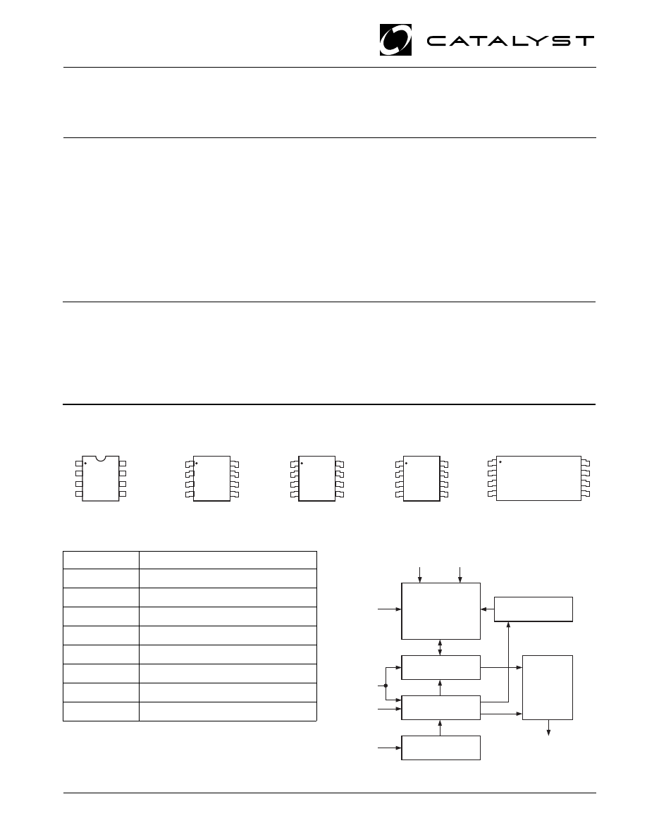
PIN CONFIGURATION
DIP Package (P)
SOIC Package (J)
manufactured using Catalyst’s advanced CMOS
E
2
PROM floating gate technology. The devices are
designed to endure 1,000,000 program/erase cycles
and have a data retention of 100 years. The devices are
available in 8-pin DIP or SOIC packages.
DESCRIPTION
The CAT93C46/56/66 are 1K/2K/4K-bit Serial E
2
PROM
memory devices which are configured as either regis-
ters of 16 bits (ORG pin at V
CC
) or 8 bits (ORG pin at
GND). Each register can be written (or read) serially by
using the DI (or DO) pin. The CAT93C46/56/66 are
SOIC Package (S)
93C46/56/66 F01
PIN FUNCTIONS
Pin Name
Function
CS
Chip Select
SK
Clock Input
DI
Serial Data Input
DO
Serial Data Output
V
CC
+1.8 to 6.0V Power Supply
GND
Ground
ORG
Memory Organization
NC
No Connection
BLOCK DIAGRAM
Note: When the ORG pin is connected to VCC, the X16 organiza-
tion is selected. When it is connected to ground, the X8 pin is
selected. If the ORG pin is left unconnected, then an internal
pullup device will select the X16 organization.
SOIC Package (K)
© 1997 by Catalyst Semiconductor, Inc.
Characteristics subject to change without notice
TSSOP Package (U)
CS
SK
DI
DO
VCC
NC
ORG
GND
1
2
3
4
8
7
6
5
CS
SK
DI
DO
VCC
NC
ORG
GND
1
2
3
4
8
7
6
5
NC
VCC
CS
SK
ORG
GND
DO
DI
1
2
3
4
8
7
6
5
CS
SK
DI
DO
VCC
NC
ORG
GND
1
2
3
4
8
7
6
5
8
7
6
5
VCC
ORG
GND
DI
CS
SK
DO
1
2
3
4
NC
VCC
ADDRESS
DECODER
MEMORY ARRAY
ORGANIZATION
128/256/512/2048X8
OR
64/128/256/1024X16
DATA
REGISTER
MODE DECODE
LOGIC
CLOCK
GENERATOR
OUTPUT
BUFFER
DO
SK
CS
DI
ORG
GND
2
CAT93C46/56/66
Stock No. 21006-03 8/97
ABSOLUTE MAXIMUM RATINGS*
Temperature Under Bias ................. –55
°
C to +125
°
C
Storage Temperature ....................... –65
°
C to +150
°
C
Voltage on any Pin with
Respect to Ground
(1)
............ –2.0V to +V
CC
+2.0V
V
CC
with Respect to Ground ............... –2.0V to +7.0V
Package Power Dissipation
Capability (Ta = 25
°
C) ................................... 1.0W
Lead Soldering Temperature (10 secs) ............ 300
°
C
Output Short Circuit Current
(2)
........................ 100 mA
*COMMENT
Stresses above those listed under “Absolute Maximum
Ratings” may cause permanent damage to the device.
These are stress ratings only, and functional operation of
the device at these or any other conditions outside of those
listed in the operational sections of this specification is not
implied. Exposure to any absolute maximum rating for
extended periods may affect device performance and
reliability.
RELIABILITY CHARACTERISTICS
Symbol
Parameter
Min.
Max.
Units
Reference Test Method
N
END
(3)
Endurance
1,000,000
Cycles/Byte
MIL-STD-883, Test Method 1033
T
DR
(3)
Data Retention
100
Years
MIL-STD-883, Test Method 1008
V
ZAP
(3)
ESD Susceptibility
2000
Volts
MIL-STD-883, Test Method 3015
I
LTH
(3)(4)
Latch-Up
100
mA
JEDEC Standard 17
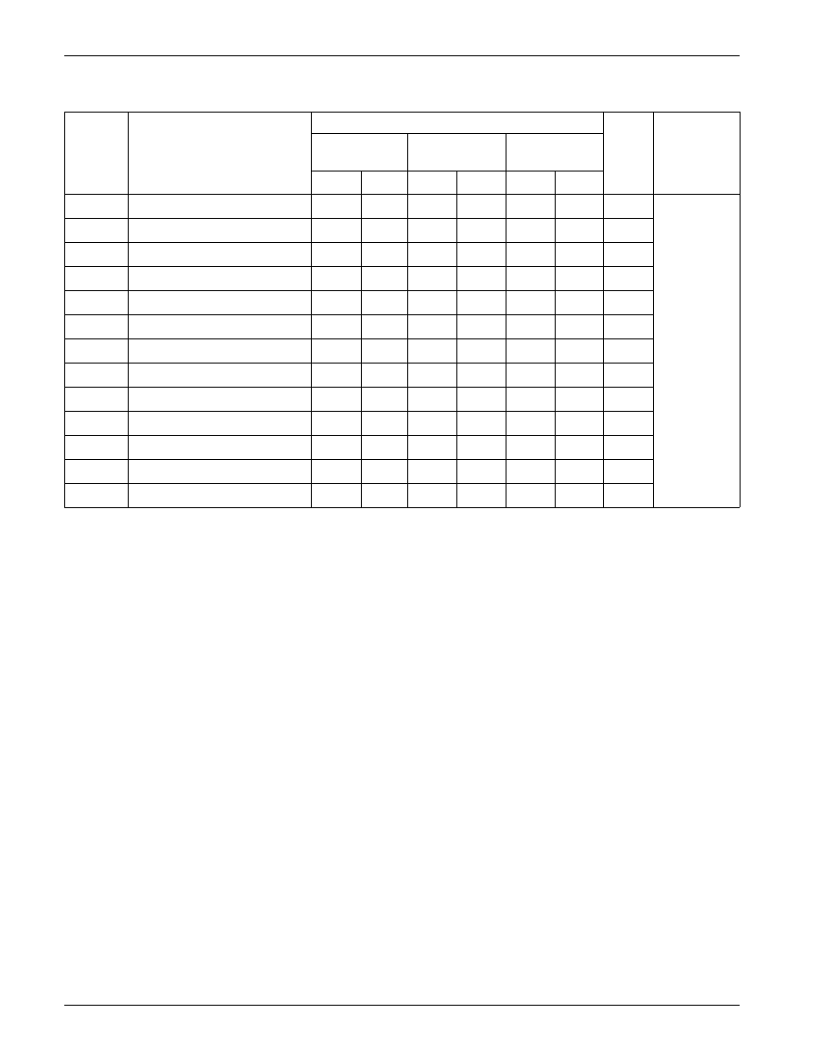
D.C. OPERATING CHARACTERISTICS
V
CC
= +1.8V to +6.0V, unless otherwise specified.
Limits
Symbol
Parameter
Min.
Typ.
Max.
Units
Test Conditions
I
CC
Power Supply Current
3
mA
DI = 0.0V, f
SK
= 1MHz
(Operating)
V
CC
= 5.0V, CS = 5.0V,
Output Open
I
SB1
Power Supply Current
25
µ
A
CS = 0V
(Standby) (x8 Mode)
ORG=GND
I
SB2
Power Supply Current
0
µ
A
CS=0V
(Standby) (x16Mode)
ORG=Float or V
CC
I
LI
Input Leakage Current
2
µ
A
V
IN
= 0V to V
CC
I
LO
Output Leakage Current
10
µ
A
V
OUT
= 0V to V
CC
,
(Including ORG pin)
CS = 0V
V
IL1
Input Low Voltage
-0.1
0.8
4.5V
≤
V
CC
<5.5V
V
IH1
Input High Voltage
2
V
CC
+1
V
IL2
Input Low Voltage
0
V
CC
X0.2
1.8V
≤
V
CC
<2.7V
V
IH2
Input High Voltage
V
CC
X0.7
V
CC
+1
V
OL1
Output Low Voltage
0.4
4.5V
≤
V
CC
<5.5V
V
OH1
Output High Voltage
2.4
I
OL
= 2.1mA
I
OH
= -400
µ
A
V
OL2
Output Low Voltage
0.2
1.8V
≤
V
CC
<2.7V
V
OH2
Output High Voltage
V
CC
-0.2
I
OL
= 1mA
I
OH
= -100
µ
A
Note:
(1) The minimum DC input voltage is –0.5V. During transitions, inputs may undershoot to –2.0V for periods of less than 20 ns. Maximum DC
voltage on output pins is V
CC
+0.5V, which may overshoot to V
CC
+2.0V for periods of less than 20 ns.
(2) Output shorted for no more than one second. No more than one output shorted at a time.
(3) This parameter is tested initially and after a design or process change that affects the parameter.
(4) Latch-up protection is provided for stresses up to 100 mA on address and data pins from –1V to V
CC
+1V.
V
V
V
V
3
CAT93C46/56/66
Stock No. 21006-03 8/97
Note:
(1) This parameter is tested initially and after a design or process change that affects the parameter.
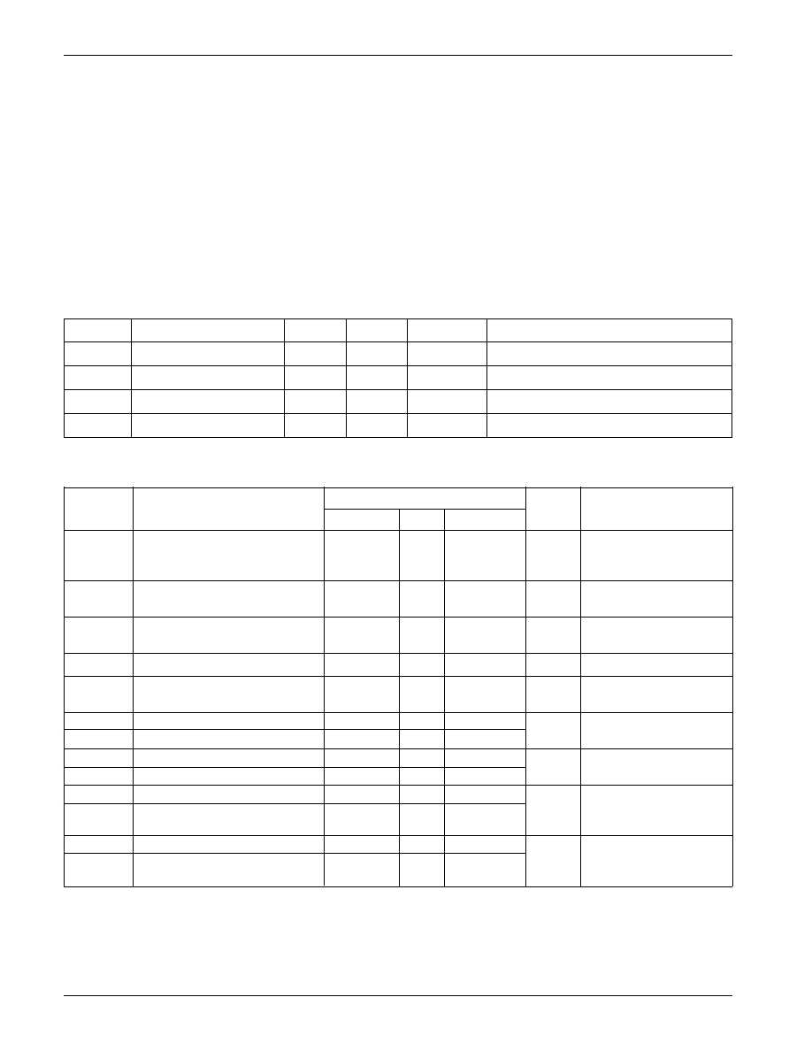
INSTRUCTION SET
Instruction Device
Start Opcode
Address Data Comments
Type
Bit
x8
x16
x8
x16
READ
93C46
1
10
A6–A0
A5-A0
Read Address AN–A0
93C56
(1)
1
10
A8–A0
A7-A0
93C66
1
10
A8–A0
A7-A0
ERASE
93C46
1
11
A6–A0
A5-A0
Clear Address AN–A0
93C56
(1)
1
11
A8–A0
A7-A0
93C66
1
11
A8–A0
A7-A0
WRITE
93C46
1
01
A6–A0
A5-A0
D7-D0
D15-D0 Write Address AN–A0
93C56
(1)
1
01
A8–A0
A7-A0
D7-D0
D15-D0
93C66
1
01
A8–A0
A7-A0
D7-D0
D15-D0
EWEN
93C46
1
00
11XXXXX
11XXXX
Write Enable
93C56
1
00
11XXXXXXX
11XXXXXX
93C66
1
00
11XXXXXXX
11XXXXXX
EWDS
93C46
1
00
00XXXXX
00XXXX
Write Disable
93C56
1
00
00XXXXXXX
00XXXXXX
93C66
1
00
00XXXXXXX
00XXXXXX
ERAL
93C46
1
00
10XXXXX
10XXXX
Clear All Addresses
93C56
1
00
10XXXXXXX
10XXXXXX
93C66
1
00
10XXXXXXX
10XXXXXX
WRAL
93C46
1
00
01XXXXX
01XXXX
D7-D0
D15-D0 Write All Addresses
93C56
1
00
01XXXXXXX
01XXXXXX
D7-D0
D15-D0
93C66
1
00
01XXXXXXX
01XXXXXX
D7-D0
D15-D0
Note:
(1) Address bit A8 for 256x8 ORG and A7 for 128x16 ORG are "Don't Care" bits, but must be kept at either a "1" or "0" for READ, WRITE and
ERASE commands.
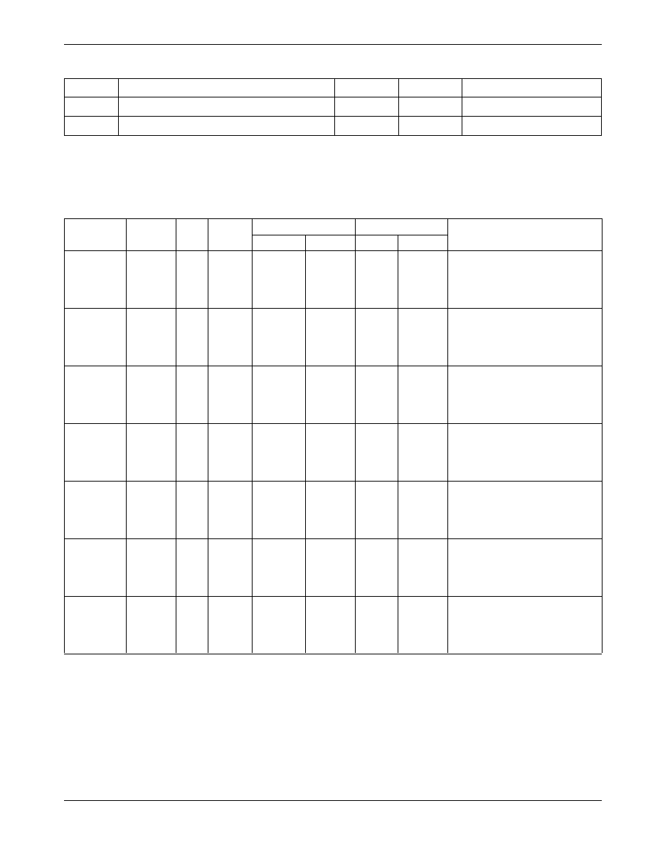
PIN CAPACITANCE
Symbol
Test
Max.
Units
Conditions
C
OUT
(1)
OUTPUT CAPACITANCE (DO)
5
pF
V
OUT
=OV
C
IN
(1)
INPUT CAPACITANCE (CS, SK, DI, ORG)
5
pF
V
IN
=OV
4
CAT93C46/56/66
Stock No. 21006-03 8/97
A.C. CHARACTERISTICS
Limits
V
CC
=
V
CC
= 2.7V -6V
V
CC
=
1.8V-6V*
V
CC
= 2.5V-6V
4.5V-5.5V
Test
SYMBOL
PARAMETER
Min.
Max.
Min.
Max.
Min.
Max.
UNITS
Conditions
t
CSS
CS Setup Time
200
100
50
ns
t
CSH
CS Hold Time
0
0
0
ns
V
IL
= 0.45V
t
DIS
DI Setup Time
400
200
100
ns
V
IH
= 2.4V
t
DIH
DI Hold Time
400
200
100
ns
C
L
= 100pF
t
PD1
Output Delay to 1
1
0.5
0.25
µ
s
V
OL
= 0.8V
t
PD0
Output Delay to 0
1
0.5
0.25
µ
s
V
OH
= 2.0v
t
HZ
(1)
Output Delay to High-Z
400
200
100
ns
t
EW
Program/Erase Pulse Width
10
10
10
ms
t
CSMIN
Minimum CS Low Time
1
0.5
0.25
µ
s
t
SKHI
Minimum SK High Time
1
0.5
0.25
µ
s
t
SKLOW
Minimum SK Low Time
1
0.5
0.25
µ
s
t
SV
Output Delay to Status Valid
1
0.5
0.25
µ
s
C
L
= 100pF
SK
MAX
Maximum Clock Frequency
DC
250
DC
500
DC
1000
KHZ
* Preliminary data for 93C56/66
NOTE:
(1) This parameter is tested initially and after a design or process change that affects the parameter.
C
L
= 100pF
5
CAT93C46/56/66
Stock No. 21006-03 8/97
DEVICE OPERATION
The CAT93C46/56/66 is a 1024/2048/4096-bit nonvola-
tile memory intended for use with industry standard
microprocessors. The CAT93C46/56/66 can be orga-
nized as either registers of 16 bits or 8 bits. When
organized as X16, seven 9-bit instructions for 93C46;
seven 11-bit instructions for 93C56 and 93C66; control
the reading, writing and erase operations of the device.
When organized as X8, seven 10-bit instructions for
93C46; seven 12-bit instructions for 93C56 and 93C66;
control the reading, writing and erase operations of the
device. The CAT93C46/56/66 operates on a single 1.8V
supply and will generate on chip, the high voltage
required during any write operation.
Instructions, addresses, and write data are clocked into
the DI pin on the rising edge of the clock (SK). The DO
pin is normally in a high impedance state except when
reading data from the device, or when checking the
ready/busy status after a write operation.
The ready/busy status can be determined after the start
of a write operation by selecting the device (CS high) and
polling the DO pin; DO low indicates that the write
operation is not completed, while DO high indicates that
the device is ready for the next instruction. If necessary,
the DO pin may be placed back into a high impedance
state during chip select by shifting a dummy “1” into the
DI pin. The DO pin will enter the high impedance state on
the falling edge of the clock (SK). Placing the DO pin into
the high impedance state is recommended in applica-
tions where the DI pin and the DO pin are to be tied
together to form a common DI/O pin.
The format for all instructions sent to the device is a
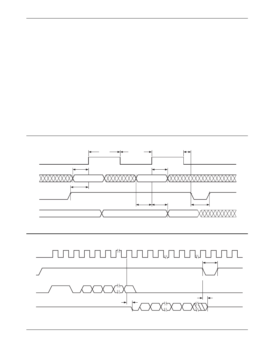
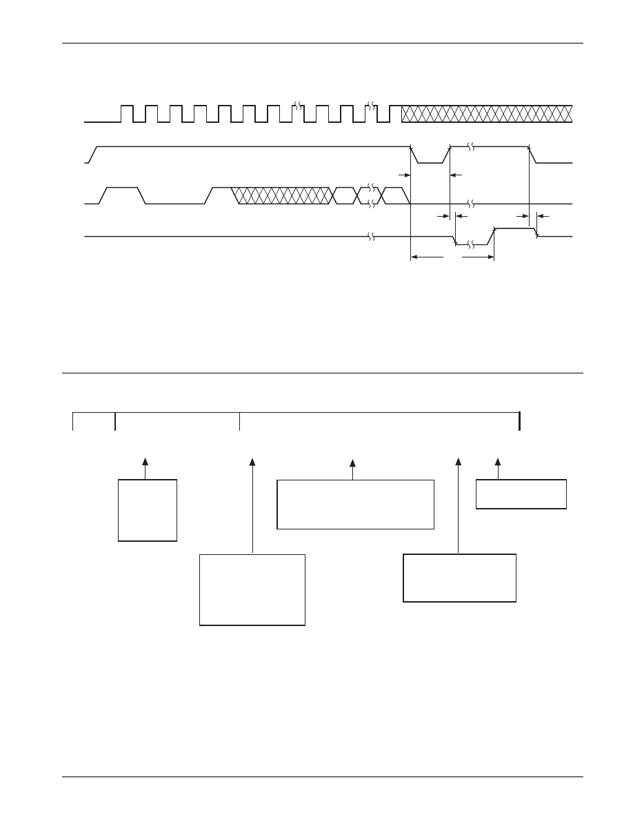
Figure 1. Sychronous Data Timing
93C46/56/66 F03
Figure 2a. Read Instruction Timing (93C46)
93C46/56/66 F04
SK
DI
CS
DO
tDIS
tPD0,tPD1
tCSMIN
tCSS
tDIS
tDIH
tSKHI
tCSH
VALID
VALID
DATA VALID
tSKLOW
SK
CS
DI
DO
tCS
STANDBY
tHZ
HIGH-Z
HIGH-Z
1
1
0
AN AN–1
A0
0
DN DN–1
D1
D0
tPD0
6
CAT93C46/56/66
Stock No. 21006-03 8/97
logical "1" start bit, a 2-bit (or 4-bit) opcode, 6-bit (93C46)/
8-bit (93C56 or 93C66) (an additional bit when orga-
nized X8) and for write operations a 16-bit data field (8-
bit for X8 organizations).
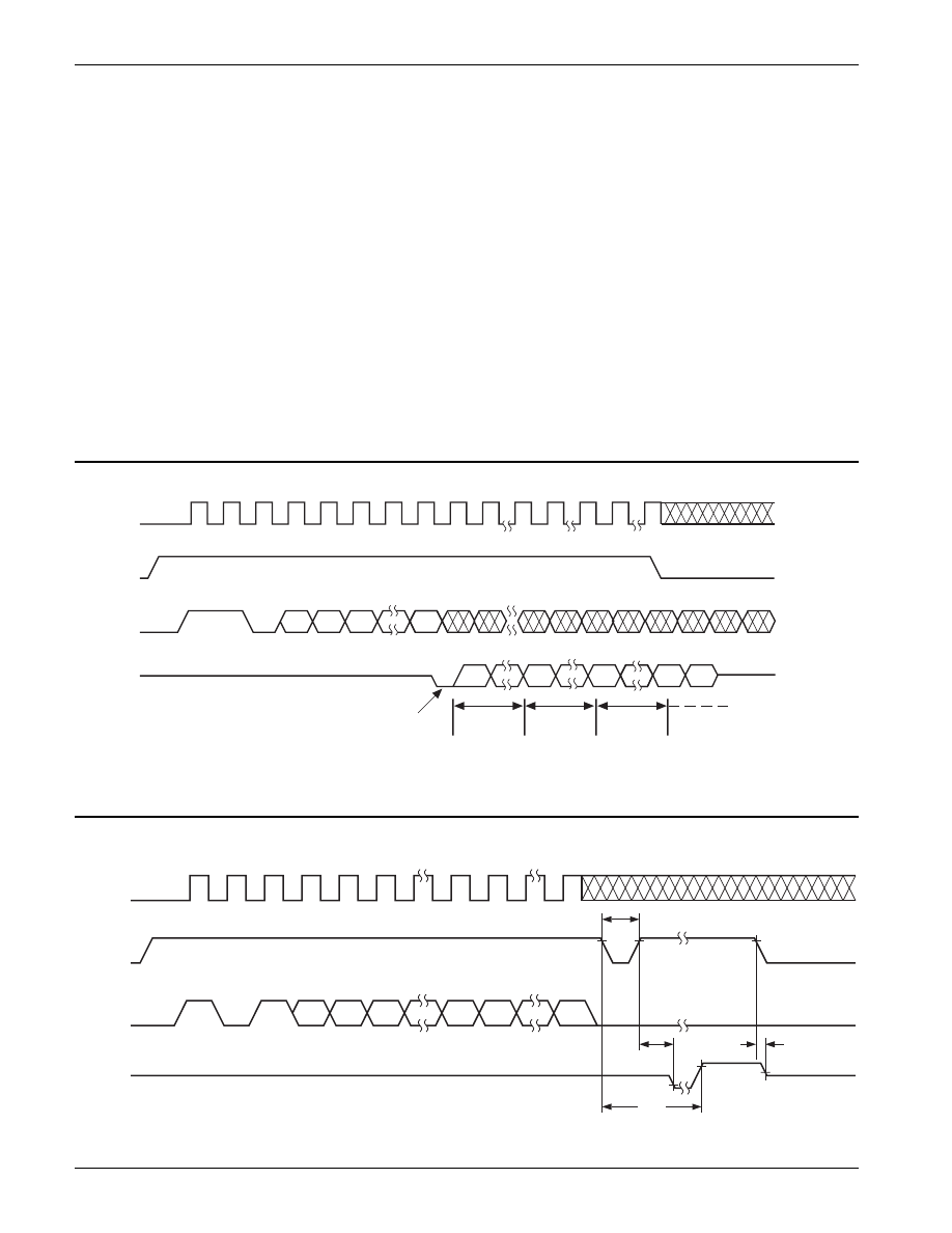
Read
Upon receiving a READ command and an address
(clocked into the DI pin), the DO pin of the CAT93C46/
56/66 will come out of the high impedance state and,
after sending an initial dummy zero bit, will begin shifting
out the data addressed (MSB first). The output data bits
will toggle on the rising edge of the SK clock and are
stable after the specified time delay (t
PD0
or t
PD1
)
For the 93C56/66, after the initial data word has been
shifted out and CS remains asserted with the SK clock
continuing to toggle, the device will automatically incre-
ment to the next address and shift out the next data word
in a sequential READ mode. As long as CS is continu-
ously asserted and SK continues to toggle, the device
will keep incrementing to the next address automatically
until it reaches to the end of the address space, then
loops back to address 0. In the sequential READ mode,
only the initial data word is preceeded by a dummy zero
bit. All subsequent data words will follow without a
dummy zero bit.
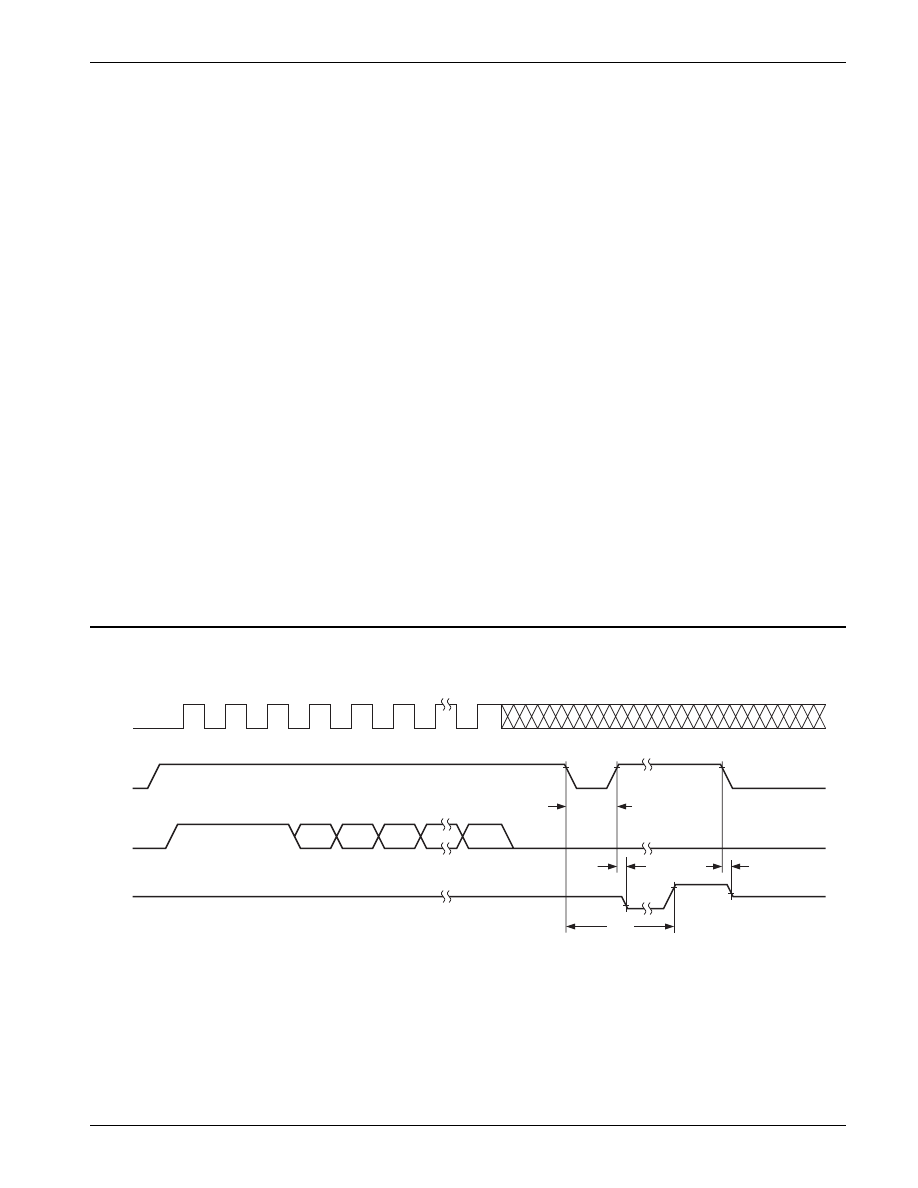
Write
After receiving a WRITE command, address and the
data, the CS (Chip Select) pin must be deselected for a
minimum of 250ns (t
CSMIN
). The falling edge of CS will
start the self clocking clear and data store cycle of the
memory location specified in the instruction. The clock-
ing of the SK pin is not necessary after the device has
entered the self clocking mode. The ready/busy status of
the CAT93C46/56/66 can be determined by selecting
the device and polling the DO pin. Since this device
features Auto-Clear before write, it is NOT necessary to
erase a memory location before it is written into.
Figure 3. Write Instruction Timing
93C46/56/66 F05
SK
CS
DI
DO
tCS
STANDBY
HIGH-Z
HIGH-Z
1
0
1
AN AN-1
A0
DN
D0
BUSY
READY
STATUS
VERIFY
tSV
tHZ
tEW
SK
CS
DI
DO
HIGH-Z
1
1
0
AN AN–1
A0
Dummy 0
D15 . . . D0
or
D7 . . . D0
1
1
1
1
1
1
1
1
1
1
1
1
1
1
1
Address + 1
D15 . . . D0
or
D7 . . . D0
Address + 2
D15 . . . D0
or
D7 . . . D0
Address + n
D15 . . .
or
D7 . . .
Don't Care
Figure 2b. Read Instruction Timing (93C56/66)
Note:
(1) The ORG pin is used to configure the device for x8 or x16 operation. When x8 organization is selected, AN = A7 and DN = D7.
When x16 organization is selected, AN = A6 and DN = D15.
7
CAT93C46/56/66
Stock No. 21006-03 8/97
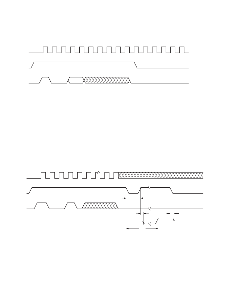
Erase
Upon receiving an ERASE command and address, the
CS (Chip Select) pin must be deasserted for a minimum
of 250ns (t
CSMIN
). The falling edge of CS will start the self
clocking clear cycle of the selected memory location.
The clocking of the SK pin is not necessary after the
device has entered the self clocking mode. The ready/
busy status of the CAT93C46/56/66 can be determined
by selecting the device and polling the DO pin. Once
cleared, the content of a cleared location returns to a
logical “1” state.
Erase/Write Enable and Disable
The CAT93C46/56/66 powers up in the write disable
state. Any writing after power-up or after an EWDS (write
disable) instruction must first be preceded by the EWEN
(write enable) instruction. Once the write instruction is
enabled, it will remain enabled until power to the device
is removed, or the EWDS instruction is sent. The EWDS
instruction can be used to disable all CAT93C46/56/66
write and clear instructions, and will prevent any acci-
dental writing or clearing of the device. Data can be read
normally from the device regardless of the write enable/
disable status.
Erase All
Upon receiving an ERAL command, the CS (Chip Se-
lect) pin must be deselected for a minimum of 250ns
(t
CSMIN
). The falling edge of CS will start the self clocking
clear cycle of all memory locations in the device. The
clocking of the SK pin is not necessary after the device
has entered the self clocking mode. The ready/busy
status of the CAT93C46/56/66 can be determined by
selecting the device and polling the DO pin. Once
cleared, the contents of all memory bits return to a logical
“1” state.
Write All
Upon receiving a WRAL command and data, the CS
(Chip Select) pin must be deselected for a minimum of
250ns (t
CSMIN
). The falling edge of CS will start the self
clocking data write to all memory locations in the device.
The clocking of the SK pin is not necessary after the
device has entered the self clocking mode. The ready/
busy status of the CAT93C46/56/66 can be determined
by selecting the device and polling the DO pin. It is not
necessary for all memory locations to be cleared before
the WRAL command is executed.
93C46/56/66 F06
Figure 4. Erase Instruction Timing
SK
CS
DI
DO
STANDBY
HIGH-Z
HIGH-Z
1
AN
AN-1
BUSY
READY
STATUS VERIFY
tSV
tHZ
tEW
tCS
1
1
A0
8
CAT93C46/56/66
Stock No. 21006-03 8/97
SK
CS
DI
STANDBY
1
0
0
*
* ENABLE=11
DISABLE=00
Figure 5. EWEN/EWDS Instruction Timing
93C46/56/66 F07
SK
CS
DI
DO
STANDBY
tCS
HIGH-Z
HIGH-Z
1
0
1
BUSY
READY
STATUS VERIFY
tSV
tHZ
tEW
0
0
Figure 6. ERAL Instruction Timing
93C46/56/66 F08
9
CAT93C46/56/66
Stock No. 21006-03 8/97
Figure 7. WRAL Instruction Timing
ORDERING INFORMATION
93C46/56/66 F10
93C46/56/66 F09
Notes:
(1) The device used in the above example is a 93C46SI-1.8TE13 (SOIC, Industrial Temperature, 1.8 Volt to 6 Volt Operating Voltage,
Tape & Reel)
STATUS VERIFY
SK
CS
DI
DO
STANDBY
HIGH-Z
1
0
1
BUSY
READY
tSV
tHZ
tEW
tCS
DN
D0
0
0
Package
P = PDIP
S = SOIC (JEDEC)
J = SOIC (JEDEC)
K = SOIC (EIAJ)
U = TSSOP
Prefix
Device #
Suffix
93C46
S
I
TE13
Product
Number
93C46: 1K
93C56: 2K
93C66: 4K
Tape & Reel
TE13: 2000/Reel
-1.8
CAT
Temperature Range
Blank = Commercial (0˚ - 70˚C)
I = Industrial (-40˚ - 85˚C)
A = Automotive (-40˚ - 105˚C)*
* -40˚ to +125˚C is available upon request
Operating Voltage
Blank (V
cc
=2.7 to 6.0V)
1.8 (V
cc
=1.8 to 6.0V)

International Sales
Offices
Europe Area
Catalyst Semiconductor, Inc.
The Quorum, Bldg. 7200
Oxford Business Park
Oxford OX4 2J2
ENGLAND
Phone: 44.1865.481.411
FAX: 44.1865.481.511
Japan Area
Nippon Catalyst K.K.
6th Fl, Kurihara Bldg.
4-48-13 Honcho
Nakano-ku, Tokyo 164
JAPAN
Phone: 81.3.5340.3781
FAX: 81.3.5340.3780
Far East Offices
Catalyst Semiconductor, Inc.
9F, No 400, Sec 1
Kee-Lung Road
Taipei, TAIWAN
Phone: 886.2.345.6192
FAX: 886.2.729.9388
Catalyst Semiconductor, Inc.
Blk 446, #B1-1635
Hougang Ave 8
Singapore 530446
Republic of Singapore
Phone: 65.385.8568
Fax: 65.385.8569
Corporate Headquarters
Catalyst Semiconductor, Inc.
1250 Borregas Avenue
Sunnyvale, CA 94089
Phone: 408-542-1000
FAX: 408-542-1200
http://www.catsemi.com
Sales Offices
Catalyst Semiconductor, Inc., 1250 Borregas Avenue, Sunnyvale, California 94089 USA, Phone: 408-542-1000, FAX: 408-542-1200, http://www.catsemi.com
U.S. Sales Offices
Western and Central U.S.
Catalyst Semiconductor, Inc.
1250 Borregas Avenue
Sunnyvale, CA 94089
Phone: 408-542-1000
FAX: 408-542-1200
Catalyst Semiconductor, Inc.
Los Gatos Eureka Building
Suite 105
236N. Santa Cruz Ave.
Los Gatos, CA 95030
Phone: 408-395-1921
FAX: 408-395-4941
Catalyst Semiconductor, Inc.
1201 S. Alma School Road
Suite 14000
Mesa, Arizona 85210
Phone: 602-844-3800
FAX: 602-844-3600
Catalyst Semiconductor, Inc.
3303 FM 1960 West
Suite 300-T
Houston, Texas 77068
Phone: 281-397-8808
FAX: 281-397-0433
Eastern U.S.
Catalyst Semiconductor, Inc.
2200 Winter Springs Blvd.
Suite 106-310
Oviedo, FL 32765
Phone: 407-977-1973
FAX: 407-977-1975
Catalyst Semiconductor, Inc.
1000 Mansell Exchange West
Suite 250
Alpharetta, GA 30022
Phone: 770-645-7541
FAX: 770-645-7551
Catalyst Semiconductor, Inc.
5669 Whitesburg Court
Norcross, GA 30092
Phone 770-613-2999
FAX: 770-613-0024
Wyszukiwarka
Podobne podstrony:
AT93C46 56 66
dominator 56;66;68;76
93LC46 56 66
akumulator do dodge s 35 46 56 66 75 s 35 46 56 66 75
Dz U 09 56 461 Warunki Techniczne zmiany
abc 56 58 Frezarki
Conan 56 Conan zwyciązca
63 66
Logistyka i Zarządzanie Łańcuchem dostaw Wykłady str 56
02 1995 56 58
56
56 Queen we are the champions
56 terapia rotacyzmu nie musi b Nieznany (2)
56[1]
65 66 607 pol ed01 2007
66 Negocjacje
2001 04 56
66 251103 projektant architekt systemow teleinformatycznych
1998 08 str 56 61 Gradientometria grawitacyjna
więcej podobnych podstron