
Signal Name
From
To
Signal Description
REF_CLK
U14
U15
26MHz System Clock
AFC
U1
U14
Automatic Frequency Control - Is used to ensure accurate frequency Information
APC
U1
U13
Automatic Powert Control - Sets the PA output level
PAENA
U7
U13
Chip enable for PowerAmp IC
HSO
U1
J5
Headset 32 ohm driver (single ended)
BATT_TEMP
U1
J1
Monitors the Battery of the Battery during Charge
BDR
U1
U7
Downlink Processed Digital Baseband Audio Information
BDX
U7
U1
Uplink Processed Digital Baseband Audio Information
BFSR
U1
U7
Baseband Data Framesynch Receive
BFSX
U7
U1
Baseband Data Framesynch Transmit
CLK13MHz _OUT
U7
U1
System Clock to Power Control IC
COL 0 - 3
U7
Keypad Matrix
Forms part of Keypad Matrix
CTS_MODEM
U7
TP9
Clear To Send
DAC
U1
BQ1
Used to allow a path to earth for VBAT through the Vibrator motor
DCS_RX
U17
U15
Received DCS Antenna Frequency Signal
DCS_PA
U13
U17
Amplified DSC PA output Transmit Frequency
DLPWR
U1
TP27/TP3
Used to Power on the unit when appropriate accessory is connnected
DSR_MODEM
U7
TP11
Data Set Ready
DTR_MODEM
U7
TP10
Data Terminal Ready
EARN
U1
Voice Receiver
Negative Audio Voice to Receiver
EARP
U1
Voice Receiver
Positive Audio Voice to Receiver
EXT_FIQ
U1
U7
Fast external interrupt for ARM
EXT_IRQ
U1
U7
External interrupt for ARM
FDP
U7
U100
The Flashreset/deeppower-downmode control,
GSM_RX
U17
U15
Received GSM Antenna Frequency Signal
GSM_TX_EN
U7
U17/U13
Used both within the RF switch and the TX VCO to select the GSM Frequency Band
GSM_PA
U13
U17
Amplified GSM PA output Transmit Frequency
EAR_DETECT
U7
J5
Headset Detect
HS_EN
U7
U11/U12
Analog switch control(MODEM or Headset)
HSMICBIAS
U1
J5
Headset Microphone bias supply(2.5V)
HSMICIP
U1
U11
Headset Microphone amplifier input (single ended)
LCDAO
U7
Display
LCD driver detect
LEDKEY_EN
U7
BQ4
When this signal goes high, the Keypad backlights are illuminated

LEDC
U1
R50
Precharge indication
MCUDI
U1
U7
ARM Input serial data.
MCUDO
U7
U1
ARM Output serial data.
MCUEN0
U7
U1
ARM Configurable enable triggers (edge/level)
MICBIAS
U1
R5
Microphone bias supply(2V)
MICIN
MIC1
U1
Negative analogue uplink audio from on board Microphone
MICIP
MIC1
U1
Positive analogue uplink audio from on board Microphone
nCHG
U5
U4
Over Voltage Protection control signal
PCHG
U1
R235
Battery Precharge Current
nBHE
U7
U24
Enable to address High Byte Information
nBLE
U7
U24
Enable to address Low Byte Information
nFOE
U7
U24, U100
Flash and SRAM output Enable - Active Low
nRESET
U7
LCD
Reset of external peripheral
nSC0
U7
U100
Used as Chip Enable for the Flash Memory
nSC1
U7
U24
Used as Chip Enable for the SRAM
PWON
U1, pin F8
S1
This signal is grounded to Earth when the Power key is pressed
RESPWRONZ
U1
U7
Chip power on reset
RF_CLK
U7
U15
Transceiver / Processer Serial Communication Data Clock
RF_DAT
To / From U7
To / From U15
Transceiver / Processer Serial Communication Data
RF_LE
U7
U15
Transceiver / Processer Serial Communication Data Latch
RTS_MODEM
U7
TP12
Request To Send.
RX_MODEM
U7
TP14/U11
Receive Data
VRF
U15
U16
Support voltage for T/R switch control
RNW
U7
U24, U100
Read and Write - allows information to be wriiten or read from the memory devices
ROW 0 - 4
U7
Keypad Matrix
Forms part of Keypad Matrix
ROW4
U7
D3
This signal is pulled low when the Power key is pressed
RTC_ALARM
U7
U1
Wakeup interrupt of real time clock
RX_IrDA
External accessory
U7
Transmitted Infra-red information from an Infrared accessory
RXIP, RXIN, RXQP,
RXQN
U15
U1
Downlink Quadrature Baseband analogue signals carrying audio information
S_PWCT
U7
R39
SIM power control
SCLK3
U7
U1
Sim Clock output from Processor
SCLK5
U1
SIM card holder
SIM data Clock
SIO3
To/From U7
To/From U1
SIM Data Communication between Processor and Power Control IC
SIO5
To/From U1
SIM card holder
Data Communications path between SIM card and Power Control IC
SRST3
U7
U1
SIM Reset from Processor

SRST5
U1
SIM card holder
SIM Reset from power Control IC
SWITCHONOFF
U1
U7
Informs the Processor that the unit has received a signal to switch on
TCXOEN
U7
U15
Xtal select(pull high for Crystal) and Xtal enable (VCXO and buffer supply)
TCK
U1
TP17U7
Scan test clock
TDI
U1
TP8/U7
Scan path input
TDO
U7
U1
Scan path output
TDR
U7
U1
Time serial port input data
TEMP_SEN
U15
U1
Temperature sense(current SW not support)
TMS
U1
U7
JTAG test mode select
TSPACT0
U7
U15
RITA Serial interface reset
TX_MODEM
U7
TP13/U12
Transmit Data
TEN
U7
U1
Time serial port enable
TRENA
U7
U16
T/R switch enable
DCS_TX
U15
U13
TX VCO generated transmit DCS Frequency
GSM_TX
U15
U13
TX VCO generated transmit GSM Frequency
TX_IrDA
U7
TP36
Transmitted Infra-red information to an Infrared accessory
TXIP, TXIN, TXQP,
TXQN
U1
U15
Uplink Quadrature Baseband analogue signals carrying audio information
VBACKUP
C38
U1
RTC battery Voltage Back up
VADCID
U1
TP29
Not use
UPR
U1
U1
Uninterrupted power rail output(VRMEM voltage selection)
VCCS
U1
U1
Charger transistor sense
VBAT
Battery Pad J1
Various
Battery Voltage for supply purposes
VCHG
Charging jack, J13
U4
Supply voltage for charging from adaptor
VCHG_VBAT
J13
U4/U5
External Power
VCHG1
U1
U1
Charger voltage sense input
VCLKRX
U1
U7
Voiceband Data transfer Clock
VDR
U1
U7
Voiceband serial port receive data
VDX
U7
U1
Voiceband serial port transmit data
VFSRX
U1
U7
Voiceband Data Frame Sychronisation Signal
D[0..15]
U7
U100/U24
Data Bus for Flash and SRAM memory
A[1..22]
U7
U100/U24
Address Bus for Flash and SRAM memory
nRESET
U7
Display
The LCM reset
VRIO_2.8V
U1
U7
For CalpysoLite_G2 power supply
VRIO_2.8V
U1
Display
LCM backlight power supply
VRIO_2.8V
U1
U11/U12
For analog switch power supply
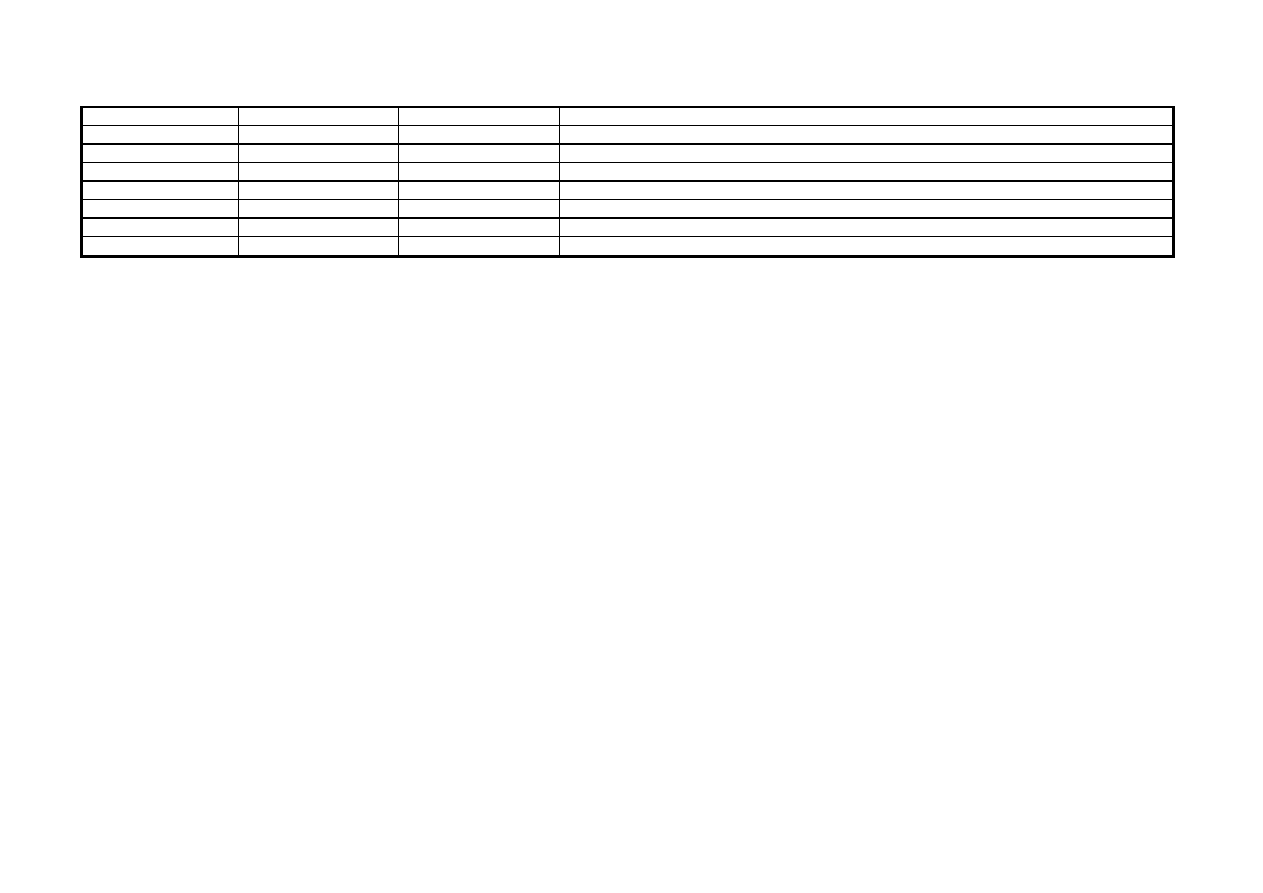
VRIO_2.8V
U1
U15
For RITA Serial interface power supply
SCL
U7
Display
I2C INTERFACE Master serial clock for LCM
SDA
U7
Display
I2C INTERFACE Serial bidirectional data for LCM
VRDBB_1.5V
U1
U7
For CalpysoLite_G2 power supply
VRRAM_2.8V
U1
U24
For SRAM power supply
VRMEM_2.8V
U1
U100
For Flash power supply
VRSIM
U1
CONN1
For SIM card power supply
VRRTC_1.5V
U1
U7
Regulator RTC output
Wyszukiwarka
Podobne podstrony:
BL C115 A4 BW L3 V1
TS V180 A4 L3 V1[1] 2
TS Triplets Refresh A4 C L3 V1[1] 1
CD P7689 A4 C L3 V1 0
CD CiDeCo E365 A4 C L3 1[1] 0 030610085958
pl v661 a4 c l3 v10
PL PaLi E365 A4 C L3 1[1] 0 030605160430
PL V3 05 A4 C L3 1 0
Parts List V200 V220 A4 C L3 8486890P01
PL V180 8486962P01 P3 A4 C L3 V1[1] 1
Circuit Description W510 A4 C L3 v1 Description
PspJEAP DCSST85 A4 C L3 Vxx
BL T193 A4 L3 BW 84D86506P03 RevB V2001 07 25
BDSD TriplestR A4 C L3 V1[1] 0
SchRF T191 1900 C A4 L3 V1 0
Sch V175 A4 C L3 1 0
PL V150 8403547B02 P3B 1 A4 C L3 V1[1] 0
DBG W206 W213 A4 C L3 V1
więcej podobnych podstron