
© Copyright 1992, 1995 National Instruments Corporation.
All Rights Reserved.
AT-MIO-16
User Manual
Multifunction I/O Board for the PC/AT
February 1995 Edition
Part Number 320476-01

National Instruments Corporate Headquarters
6504 Bridge Point Parkway
Austin, TX 78730-5039
(512) 794-0100
Technical support fax:
(800) 328-2203
(512) 794-5678
Branch Offices:
Australia (03) 879 9422, Austria (0662) 435986, Belgium 02/757.00.20, Canada (Ontario) (519) 622-9310,
Canada (Québec) (514) 694-8521, Denmark 45 76 26 00, Finland (90) 527 2321, France (1) 48 14 24 24,
Germany 089/741 31 30, Italy 02/48301892, Japan (03) 3788-1921, Mexico 95 800 010 0793,
Netherlands 03480-33466, Norway 32-84 84 00, Singapore 2265886, Spain (91) 640 0085, Sweden 08-730 49 70,
Switzerland 056/20 51 51, Taiwan 02 377 1200, U.K. 0635 523545

Limited Warranty
The AT-MIO-16 is warranted against defects in materials and workmanship for a period of one year from the date of
shipment, as evidenced by receipts or other documentation. National Instruments will, at its option, repair or replace
equipment that proves to be defective during the warranty period. This warranty includes parts and labor.
The media on which you receive National Instruments software are warranted not to fail to execute programming
instructions, due to defects in materials and workmanship, for a period of 90 days from date of shipment, as
evidenced by receipts or other documentation. National Instruments will, at its option, repair or replace software
media that do not execute programming instructions if National Instruments receives notice of such defects during
the warranty period. National Instruments does not warrant that the operation of the software shall be uninterrupted
or error free.
A Return Material Authorization (RMA) number must be obtained from the factory and clearly marked on the
outside of the package before any equipment will be accepted for warranty work. National Instruments will pay the
shipping costs of returning to the owner parts which are covered by warranty.
National Instruments believes that the information in this manual is accurate. The document has been carefully
reviewed for technical accuracy. In the event that technical or typographical errors exist, National Instruments
reserves the right to make changes to subsequent editions of this document without prior notice to holders of this
edition. The reader should consult National Instruments if errors are suspected. In no event shall National
Instruments be liable for any damages arising out of or related to this document or the information contained in it.
E
XCEPT AS SPECIFIED HEREIN
, N
ATIONAL
I
NSTRUMENTS MAKES NO WARRANTIES
,
EXPRESS OR IMPLIED
,
AND SPECIFICALLY DISCLAIMS ANY WARRANTY OF MERCHANTABILITY OR FITNESS FOR A PARTICULAR
PURPOSE
. C
USTOMER
'
S RIGHT TO RECOVER DAMAGES CAUSED BY FAULT OR NEGLIGENCE ON THE PART
OF
N
ATIONAL
I
NSTRUMENTS SHALL BE LIMITED TO THE AMOUNT THERETOFORE PAID BY THE CUSTOMER
.
N
ATIONAL
I
NSTRUMENTS WILL NOT BE LIABLE FOR DAMAGES RESULTING FROM LOSS OF DATA
,
PROFITS
,
USE OF PRODUCTS
,
OR INCIDENTAL OR CONSEQUENTIAL DAMAGES
,
EVEN IF ADVISED OF THE POSSIBILITY
THEREOF
. This limitation of the liability of National Instruments will apply regardless of the form of action,
whether in contract or tort, including negligence. Any action against National Instruments must be brought within
one year after the cause of action accrues. National Instruments shall not be liable for any delay in performance due
to causes beyond its reasonable control. The warranty provided herein does not cover damages, defects,
malfunctions, or service failures caused by owner's failure to follow the National Instruments installation, operation,
or maintenance instructions; owner's modification of the product; owner's abuse, misuse, or negligent acts; and
power failure or surges, fire, flood, accident, actions of third parties, or other events outside reasonable control.
Copyright
Under the copyright laws, this publication may not be reproduced or transmitted in any form, electronic or
mechanical, including photocopying, recording, storing in an information retrieval system, or translating, in whole or
in part, without the prior written consent of National Instruments Corporation.
Trademarks
LabVIEW
®
, NI-DAQ
®
, and RTSI
®
are trademarks of National Instruments Corporation.
Product and company names listed are trademarks or trade names of their respective companies.

WARNING REGARDING MEDICAL AND CLINICAL USE
OF NATIONAL INSTRUMENTS PRODUCTS
National Instruments products are not designed with components and testing intended to ensure a level of reliability
suitable for use in treatment and diagnosis of humans. Applications of National Instruments products involving
medical or clinical treatment can create a potential for accidental injury caused by product failure, or by errors on the
part of the user or application designer. Any use or application of National Instruments products for or involving
medical or clinical treatment must be performed by properly trained and qualified medical personnel, and all
traditional medical safeguards, equipment, and procedures that are appropriate in the particular situation to prevent
serious injury or death should always continue to be used when National Instruments products are being used.
National Instruments products are NOT intended to be a substitute for any form of established process, procedure, or
equipment used to monitor or safeguard human health and safety in medical or clinical treatment.

© National Instruments Corporation
v
AT-MIO-16 User Manual
Contents
Conventions Used in This Manual ...............................................................................
x
x
Customer Communication ...........................................................................................
x
LabVIEW and LabWindows Application Software ........................................
Chapter 2
Configuration and Installation
.....................................................................................
Base I/O Address Selection..................................................................
DMA Channel Selection ......................................................................
Interrupt Selection ................................................................................
Analog Input Configuration .................................................................
Input Mode ...............................................................................
DIFF Input (Eight Channels, Factory Setting) .............
RSE Input (16 Channels) .............................................
NRSE Input (16 Channels) ..........................................
Analog Input Polarity and Range .............................................
Considerations for Selecting Input Ranges. .................
Analog Output Configuration ..............................................................
Analog Output Reference.........................................................
Analog Output Polarity Selection ............................................
Analog Output Data Coding ....................................................

Contents
AT-MIO-16 User Manual
vi
© National Instruments Corporation
Analog Input Signal Connections ........................................................
Types of Signal Sources.......................................................................
Floating Signal Sources ...........................................................
Ground-Referenced Signal Sources .........................................
Input Configurations ............................................................................
Differential Connections for Grounded Signal Sources ..........
Differential Connections for Floating Signal Sources .............
Single-Ended Connection Considerations ...............................
Common-Mode Signal Rejection Considerations....................
Analog Output Signal Connections......................................................
Data Acquisition Timing Connections.................................................
General-Purpose Timing Signal Connections ......................................
Chapter 4
Calibration Procedures
....................................................................................................
Bipolar Input Calibration Procedure ................................................................
1. Adjust the Amplifier Input Offset ...................................................
2. Adjust the ADC Input Offset ..........................................................
3. Adjust the Analog Input Gain .........................................................
Unipolar Input Calibration Procedure ..............................................................
1. Adjust the Amplifier Input Offset ...................................................
2. Adjust the ADC Input Offset ..........................................................
3. Adjust the Analog Input Gain .........................................................
Bipolar Output Calibration Procedure .............................................................
1. Adjust the Analog Output Offset ....................................................
2. Adjust the Analog Output Gain ......................................................
Unipolar Output Calibration Procedure ...........................................................
1. Adjust the Analog Output Offset ....................................................
2. Adjust the Analog Output Gain ......................................................

Contents
© National Instruments Corporation
vii
AT-MIO-16 User Manual
Appendix B
Revisions A through C Parts Locator Diagram
....................................................
Appendix C
Customer Communication
............................................................................................
Index-1
Figures
AT-MIO-16 Parts Locator Diagram ................................................................
Example Base I/O Address Switch Settings ....................................................
Analog Input and Data Acquisition Circuitry Block Diagram ........................
Analog Output Circuitry Block Diagram .........................................................
Digital I/O Circuitry Block Diagram ...............................................................
AT-MIO-16 I/O Connector Pin Assignments ..................................................
AT-MIO-16 Instrumentation Amplifier ...........................................................
Differential Input Connections for Grounded Signal Sources .........................
Differential Input Connections for Floating Signal Sources............................
Single-Ended Input Connections for Floating Signal Sources.........................
Single-Ended Input Connections for Grounded Signal Sources ......................
RTSI Bus Interface Circuitry Block Diagram..................................................
Figure 3-16. Event-Counting Application with External Switch Gating..............................
Calibration Trimpot Location Diagram ...........................................................
Revisions A through C Parts Locator Diagram ...............................................

Contents
AT-MIO-16 User Manual
viii
© National Instruments Corporation
Tables
AT Bus Interface Factory-Default Settings .....................................................
Analog I/O Jumper Settings Quick Reference .................................................
DIFF Input Configuration (Factory Setting) ....................................................
Configurations for Input Range and Input Polarity .........................................
Table 2-10. Actual Range and Measurement Precision Versus Input Range
Table 2-12. Analog Output Polarity and Data Mode Configuration ...................................
Voltage Values for Calculating Offset Error ...................................................

© National Instruments Corporation
ix
AT-MIO-16 User Manual
About This Manual
This manual describes the electrical and mechanical aspects of the AT-MIO-16 and contains
information concerning its operation and programming. The AT-MIO-16 is a high-performance
multifunction analog, digital, and timing I/O board, and is a member of the National Instruments
AT Series of expansion boards for the IBM PC AT and compatible computers. The AT-MIO-16
contains a 12-bit ADC with up to 16 analog inputs, two 12-bit DACs with voltage outputs, eight
lines of TTL-compatible digital I/O, and three 16-bit counter/timer channels for timing I/O. If
you need additional analog inputs, you can use the AMUX-64T multiplexer board, which is a
four-to-one multiplexer that can process 64 single-ended inputs. You can cascade up to four
AMUX-64Ts to obtain 256 single-ended inputs.
Organization of This Manual
The AT-MIO-16 User Manual is organized as follows:
•
Chapter 1, Introduction, describes the AT-MIO-16; lists the contents of your AT-MIO-16 kit,
the optional software, and optional equipment; and explains how to unpack the AT-MIO-16.
•
Chapter 2, Configuration and Installation, describes how to configure the AT-MIO-16
jumpers and how to install the AT-MIO-16 board into the PC.
•
Chapter 3, Signal Connections, describes the signal connections to the AT-MIO-16 board,
and cable wiring.
•
Chapter 4, Calibration Procedures, discusses the calibration procedures for the AT-MIO-16
analog input and analog output circuitry.
•
Appendix A, Specifications, lists the specifications for the AT-MIO-16.
•
Appendix B, Revisions A through C Parts Locator Diagram, contains the parts locator
diagram for revisions A through C of the AT-MIO-16 board.
•
Appendix C, Customer Communication, contains forms you can use to request help from
National Instruments or to comment on our products.
•
The Glossary contains an alphabetical list and description of terms used in this manual,
including acronyms, abbreviations, metric prefixes, mnemonics, and symbols.
•
The Index alphabetically lists topics covered in this manual, including the page where you
can find the topic.

About This Manual
AT-MIO-16 User Manual
x
© National Instruments Corporation
Conventions Used in This Manual
The following conventions are used in this manual.
bold italic
Bold italic text denotes a note, caution, or warning.
italic
Italic text denotes emphasis, a cross reference, or an introduction to a key
concept.
NI-DAQ
NI-DAQ is used throughout this manual to refer to the NI-DAQ software
for PC compatibles unless otherwise noted.
PC
PC refers to the IBM PC AT and compatible computers.
Abbreviations, acronyms, metric prefixes, mnemonics, symbols, and terms are listed in the
Glossary.
Related Documentation
The following document contains information that you may find helpful as you read this manual:
•
IBM Personal Computer AT Technical Reference manual
You may also want to consult the following Advanced Micro Devices manual if you plan to
program the Am9513A counter/timer used on the AT-MIO-16:
•
Am9513A/Am9513 System Timing Controller technical manual
National Instruments offers a register-level programmer manual at no charge to customers who
are not using National Instruments software:
•
AT-MIO-16 Register-Level Programmer Manual
If you are using NI-DAQ, LabVIEW, or LabWindows
®
, you should not need the register-level
programmer manual. Using NI-DAQ, LabVIEW, or LabWindows is quicker and easier than and
as flexible as using the low-level programming described in the register-level programmer
manual. Refer to Software Programming Choices in Chapter 1, Introduction, of this manual if
you need more information about your programming options.
If you are not using National Instruments software, you can request the register-level
programmer manual by mailing or faxing the Register-Level Programmer Manual Request Form
at the back of this manual to National Instruments.
Customer Communication
National Instruments wants to receive your comments on our products and manuals. We are
interested in the applications you develop with our products, and we want to help if you have
problems with them. To make it easy for you to contact us, this manual contains comment and
configuration forms for you to complete. These forms are in Appendix C, Customer
Communication, at the end of this manual.

© National Instruments Corporation
1-1
AT-MIO-16 User Manual
Chapter 1
Introduction
This chapter describes the AT-MIO-16; lists the contents of your AT-MIO-16 kit; describes the
optional software and optional equipment; and explains how to unpack the AT-MIO-16.
About the AT-MIO-16
Congratulations on your purchase of the National Instruments AT-MIO-16. The AT-MIO-16 is a
high-performance, software-configurable 12-bit DAQ board for laboratory, test and
measurement, and data acquisition and control applications. The board performs high-accuracy
measurements with high-speed settling to 12 bits, noise as low as 0.1 LSBrms, and a typical
DNL of
±
0.5 LSB. Because of its FIFOs and dual-channel DMA, the AT-MIO-16 can achieve
high performance, even when used in environments that may have long interrupt latencies such
as Windows.
A common problem with DAQ boards is that you cannot easily synchronize several
measurement functions to a common trigger or timing event. The AT-MIO-16 has the Real-
Time System Integration (RTSI) bus to solve this problem. The RTSIbus consists of our custom
RTSI bus interface chip and a ribbon cable to route timing and trigger signals between several
functions on one or DAQ boards in your PC.
The AT-MIO-16 can interface to the Signal Conditioning eXtensions for Instrumentation (SCXI)
system so that you can acquire over 3,000 analog signals from thermocouples, RTDs, strain
gauges, voltage sources, and current sources. You can also acquire or generate digital signals for
communication and control. SCXI is the instrumentation front-end for plug-in DAQ boards.
What You Need to Get Started
Two versions of the AT-MIO-16 are available–one version for each of two gain ranges. The
AT-MIO-16L (L stands for low-level signals) has software-programmable gain settings of 1, 10,
100, and 500 for low-level analog input signals. The AT-MIO-16H (H stands for high-level
signals) has software-programmable gain settings of 1, 2, 4, and 8 for high-level analog input
signals. The AT-MIO-16(L/H)-9 contains an ADC with a 9
µ
s conversion time. The
AT-MIO-16(L/H)-9 is capable of data acquisition rates of up to 100 kHz.
To set up and use your AT-MIO-16 board, you will need the following:
An AT-MIO-16 board
AT-MIO-16 User Manual

Introduction
Chapter 1
AT-MIO-16 User Manual
1-2
© National Instruments Corporation
Either of the following software:
NI-DAQ software for PC compatibles, with manuals
LabVIEW for Windows, LabWindows for DOS, or LabWindows/CVI for Windows,
with manuals
Your computer
Detailed specifications of the AT-MIO-16 are listed in Appendix A, Specifications.
Software Programming Choices
There are four options to choose from when programming your National Instruments plug-in
DAQ and SCXI hardware. You can use LabVIEW, LabWindows, NI-DAQ, or register-level
programming software.
The AT-MIO-16 works with LabVIEW for Windows, LabWindows for DOS, LabWindows/CVI
for Windows, and NI-DAQ for PC compatibles.
LabVIEW and LabWindows Application Software
LabVIEW and LabWindows are innovative program development software packages for data
acquisition and control applications. LabVIEW uses graphical programming, whereas
LabWindows enhances traditional programming languages. Both packages include extensive
libraries for data acquisition, instrument control, data analysis, and graphical data presentation.
LabVIEW currently runs on four different platforms—AT/MC/EISA computers running
Microsoft Windows, NEC 9800 computers running Microsoft Windows, the Macintosh platform,
and the Sun SPARCstation platform. LabVIEW features interactive graphics, a state-of-the-art
user interface, and a powerful graphical programming language. The LabVIEW Data
Acquisition VI Library, a series of VIs for using LabVIEW with National Instruments boards, is
included with LabVIEW. The LabVIEW Data Acquisition VI Libraries are functionally
equivalent to the NI-DAQ software.
LabWindows has two versions—LabWindows for DOS is for use on PCs running DOS, and
LabWindows/CVI is for use on PCs running Windows and Sun SPARCstations.
LabWindows/CVI features interactive graphics, a state-of-the-art user interface, and uses the
ANSI standard C programming language. The LabWindows Data Acquisition Library, a series
of functions for using LabWindows with National Instruments boards, is included with
LabWindows for DOS and LabWindows/CVI. The LabWindows Data Acquisition libraries are
functionally equivalent to the NI-DAQ software.
Using LabVIEW or LabWindows software will greatly diminish the development time for your
data acquisition and control application.

Chapter 1
Introduction
© National Instruments Corporation
1-3
AT-MIO-16 User Manual
NI-DAQ Driver Software
The NI-DAQ driver software is included at no charge with all National Instruments DAQ
hardware. NI-DAQ is not packaged with SCXI or accessory products, except for the SCXI-1200.
NI-DAQ has an extensive library of functions that you can call from your application
programming environment. These functions include routines for analog input (A/D conversion),
buffered data acquisition (high-speed A/D conversion), analog output (D/A conversion),
waveform generation, digital I/O, counter/timer operations, SCXI, RTSI, self-calibration,
messaging, and acquiring data to extended memory.
NI-DAQ has both high-level DAQ I/O functions for maximum ease of use and low-level data
acquisition I/O functions for maximum flexibility and performance. Examples of high-level
functions are streaming data to disk or acquiring a certain number of data points. An example of
a low-level function is writing directly to registers on the data acquisition device. NI-DAQ does
not sacrifice the performance of National Instruments data acquisition devices because it lets
multiple devices operate at their peak performance—up to 500 kS/s on ISA computers and up to
1 MS/s on EISA computers.
NI-DAQ includes a Buffer and Data Manager that uses sophisticated techniques for handling
and managing data acquisition buffers so that you can simultaneously acquire and process data.
NI-DAQ functions for the AT-MIO-16 can transfer data using interrupts or software polling.
With the NI-DAQ Resource Manager, you can simultaneously use several functions and several
DAQ devices. The Resource Manager prevents multiple-device contention over DMA channels,
interrupt levels, and RTSI channels.
NI-DAQ can send event-driven messages to DOS, Windows, or Windows NT applications
whenever a user-specified event occurs. Thus, polling is eliminated and you can develop event-
driven data acquisition applications. An example of a NI-DAQ user event is when a specified
digital I/O pattern is matched.
NI-DAQ also internally addresses many of the complex issues between the computer and the
DAQ hardware such as programming interrupts and DMA controllers. NI-DAQ maintains a
consistent software interface among its different versions so that you can change platforms with
minimal modifications to your code. Figure 1-1 illustrates the relationship between NI-DAQ and
LabVIEW and LabWindows. You can see that the data acquisition parts of LabVIEW and
LabWindows are functionally equivalent to the NI-DAQ software.
Introduction
Chapter 1
AT-MIO-16 User Manual
1-4
© National Instruments Corporation
LabWindows
(PC or
Sun SPARCstation)
LabVIEW
(PC, Macintosh, or
Sun SPARCstation)
Conventional
Programming
Environment
(PC, Macintosh, or
Sun SPARCstation)
NI-DAQ
Driver Software
DAQ or
SCXI Hardware
Personal
Computer
or
Workstation
Figure 1-1. The Relationship between the Programming Environment,
NI-DAQ, and Your Hardware
The National Instruments PC, AT, MC, EISA, DAQCard, and
DAQPad Series DAQ hardware
and the SCXI-1200 are packaged with NI-DAQ software for PC compatibles. NI-DAQ software
for PC compatibles comes with language interfaces for Professional BASIC, QuickBASIC,
Visual Basic, Borland Turbo Pascal, Turbo C++, Borland C++, Microsoft Visual C++, and
Microsoft C for DOS; and Visual Basic, Turbo Pascal, Microsoft C with SDK, Microsoft Visual
C++, and Borland C++ for Windows; and Microsoft Visual C++ for Windows NT. You can use
your AT-MIO-16, together with other PC, AT, MC, EISA, DAQCard, and DAQPad Series DAQ
and SCXI hardware, with NI-DAQ software for PC compatibles.
The National Instruments NB Series DAQ boards are packaged with NI-DAQ software for
Macintosh. NI-DAQ software for Macintosh comes with language interfaces for MPW C,
THINK C, Pascal, and Microsoft QuickBASIC. Any language that uses Device Manager
Toolbox calls can access NI-DAQ software for Macintosh. You can use NB Series DAQ boards
and SCXI hardware with NI-DAQ software for Macintosh.
The National Instruments SB Series DAQ boards are packaged with NI-DAQ software for Sun,
which comes with a language interface for ANSI C.

Chapter 1
Introduction
© National Instruments Corporation
1-5
AT-MIO-16 User Manual
Register-Level Programming
The final option for programming any National Instruments DAQ hardware is to write register-
level software. Writing register-level programming software can be very time consuming and
inefficient, and is not recommended for most users. The only users who should consider writing
register-level software should meet at least one of the following criteria:
•
National Instruments does not support your operating system or programming language.
•
You are an experienced register-level programmer who is more comfortable writing your
own register-level software.
Even if you are an experienced register-level programmer, consider using NI-DAQ, LabVIEW,
or LabWindows to program your National Instruments DAQ hardware. Using the NI-DAQ,
LabVIEW, or LabWindows software is easier than, is as flexible as, and can save weeks of
development time.
The AT-MIO-16 User Manual and your software manuals contains complete instructions for
programming your AT-MIO-16 board with NI-DAQ, LabVIEW, or LabWindows. If you are
using NI-DAQ, LabVIEW, or LabWindows to control your board, you should not need the
register-level programmer manual.
The AT-MIO-16 Register-Level Programmer Manual contains low-level programming details,
such as register maps, bit descriptions, and register programming hints, that you will need only
for register-level programming. If you want to obtain the register-level programmer manual,
please fill out the Register-Level Programmer Manual Request Form at the end of this manual
and send it to National Instruments.
Unpacking
Your AT-MIO-16 board is shipped in an antistatic package to prevent electrostatic damage to the
board. Electrostatic discharge can damage several components on the board. To avoid such
damage in handling the board, take the following precautions:
•
Ground yourself via a grounding strap or by holding a grounded object.
•
Touch the antistatic package to a metal part of your computer chassis before removing the
board from the package.
•
Remove the board from the package and inspect the board for loose components or any other
sign of damage. Notify National Instruments if the board appears damaged in any way. Do
not install a damaged board into your computer.
•
Never touch the exposed pin of connectors.
© National Instruments Corporation
2-1
AT-MIO-16 User Manual
Chapter 2
Configuration and Installation
This chapter describes how to configure the AT-MIO-16 jumpers and how to install the
AT-MIO-16 board into the PC.
Board Configuration
The AT-MIO-16 contains 13 jumpers and one DIP switch to configure the AT bus interface and
analog I/O settings. The DIP switch is for setting the base I/O address. Two jumpers are
interrupt channel and DMA selectors. The remaining 11 jumpers change the analog input and
analog output circuitry. The parts locator diagram in Figure 2-1 shows the user-configurable
jumpers. Jumpers W1, W4, W6, and W9 configure the analog input circuitry. Jumpers W2, W3,
W7, W8, W10, and W11 configure the analog output circuitry. Jumper W5 selects the clock
signal the Am9513A counter/timer uses and selects the clock pin on the RTSI bus. Jumpers W12
and W13 select the DMA channel and the interrupt level, respectively.
AT Bus Interface
The AT-MIO-16 is configured at the factory to a base I/O address of hex 220, to use DMA
channels 6 and 7, and to use interrupt level 10. These settings, as shown in Table 2-1, are
suitable for most systems. If your system, however, has other hardware at this base I/O address,
DMA channel, or interrupt level, you will need to change these settings on the other hardware or
on the AT-MIO-16 as described in the following pages.
Table 2-1. AT Bus Interface Factory-Default Settings
AT-MIO-16 Board
Default Setting
Hardware Implementation
Base I/O address
U61
Hex 220
Range: hex 220 to hex 23F
U61
1 2
3 4 5
A9
A8
A7
A6
A5
Address space
32 bytes (hex 20)
DMA channel
W12
DMA 1 = DMA channel 6
DMA 2 = DMA channel 7
R7
A7
R6
A6
R5
A5
W12
1 DMA 2
Interrupt level
W13
Interrupt level 10 selected
3
4
5
6 7
9 10 11 12 14 15
IRQ
W13
Chapter 2
Configuration and Installation
© National Instruments Corporation
2-3
AT-MIO-16 User Manual
Note: The parts locator diagram shown in Figure 2-1 is for revision D and subsequent
revisions of the AT-MIO-16 board. See Appendix B, Revisions A through C Parts
Locator Diagram, for earlier revisions of the AT-MIO-16 board. The remainder of this
chapter applies to all revisions of the AT-MIO-16 board.
In the configuration illustrations throughout this chapter, the black bars on the jumper diagrams
indicate where to place jumpers. On the switch diagrams, the shaded portion indicates the side of
the switch that is pressed down.
Base I/O Address Selection
The switches at position U61 determine the base I/O address for the AT-MIO-16, as shown in
Figure 2-1. Each switch in U61 corresponds to one of the address lines A9 through A5. Press
the side marked OFF to select a binary value of 1 for the corresponding address bit. Press the
other side of the switch to select a binary value of 0 for the corresponding address bit. Figure 2-2
shows two possible switch settings.
Note:
Verify that other equipment installed in your computer does not already occupy the
AT-MIO-16 address space. If any equipment in your computer uses this base I/O
address space, you must change the base I/O address of either the AT-MIO-16 or that
of the other device. If you change the AT-MIO-16 base I/O address, you must make
a corresponding change to any software you use with the AT-MIO-16. For more
information about the I/O address of your PC AT, refer to the technical reference
manual for your computer.
This side down for 0
This side down for 0
U61
1 2
3 4 5
A9
A8
A7
A6
A5
U61
1 2
3 4 5
A9
A8
A7
A6
A5
This side down for 1
This side down for 1
a. Switches Set to Base I/O
Address of Hex 000
b. Switches Set to Base I/O Address of Hex
220 (Factory Setting)
Figure 2-2. Example Base I/O Address Switch Settings
To change the base I/O address, remove the plastic cover on U61; press each switch to the
desired position; check each switch to make sure the switch is pressed down all the way; and
replace the plastic cover. Make a note of the new AT-MIO-16 base I/O address on the
configuration form in Appendix C, Customer Communication, to use when configuring the
software you are using with the AT-MIO-16. Table 2-2 lists the possible switch settings, the
corresponding base I/O address, and the base I/O address space for each setting.
Configuration and Installation
Chapter 2
AT-MIO-16 User Manual
2-4
© National Instruments Corporation
Table 2-2. Switch Settings with Corresponding Base I/O Address and Base I/O Address Space
Switch Setting
Base I/O Address
Base I/O Address
A9
A8
A7
A6
A5
(hex)
Space Used (hex)
0
1
1
0
0
180
180-19F
0
1
1
0
1
1A0
1A0-1BF
0
1
1
1
0
1C0
1C0-1DF
0
1
1
1
1
1E0
1E0-1FF
1
0
0
0
0
200
200-21F
1
0
0
0
1
220
220-23F
1
0
0
1
0
240
240-25F
1
0
0
1
1
260
260-27F
1
0
1
0
0
280
280-29F
1
0
1
0
1
2A0
2A0-2BF
1
0
1
1
0
2C0
2C0-2DF
1
0
1
1
1
2E0
2E0-2FF
1
1
0
0
0
300
300-31F
1
1
0
0
1
320
320-33F
1
1
0
1
0
340
340-35F
1
1
0
1
1
360
360-37F
1
1
1
0
0
380
380-39F
1
1
1
0
1
3A0
3A0-3BF
1
1
1
1
0
3C0
3C0-3DF
1
1
1
1
1
3E0
3E0-3FF
Note:
Base I/O address values hex 000 through 0FF are reserved for
system use. Base I/O address values hex 100 through 3FF are
available on the I/O channel.
DMA Channel Selection
The AT-MIO-16 uses the DMA channel you select with the jumpers on W12 as shown in
Figure 2-1. The AT-MIO-16 is set at the factory to use DMA channels 6 and 7. Verify that
equipment already installed in your computer does not also use these DMA channels. If any
device uses DMA channel 6 or 7, change or disable the DMA channel or channels of either the
AT-MIO-16 or the other device. The AT-MIO-16 hardware supports DMA channels 5, 6, and 7.
Notice that these are the three 16-bit channels on the PC AT I/O channel. The AT-MIO-16 does
not use and cannot be configured to use the 8-bit DMA channels on the PC AT I/O channel.
You must install two jumpers on W12 to select a DMA channel. The DMA Acknowledge lines
(A- prefix is printed on the board) and the DMA Request lines (R- prefix is printed on the board)
that you select must have the same number suffix (5, 6, or 7) for proper operation. When you
enable two DMA channels, the driver software has the option of using dual DMA mode, which
may improve performance in high-rate data acquisition. However, data acquisition can operate
properly with one or both DMA channels disabled. Disabling DMA 2 or disabling both DMA
channels may be necessary if no more DMA channels are available on your system. If two
AT-MIO-16s are installed in the same computer, for instance, you must disable DMA 2 on one
of the boards. The left two columns of W12 are for DMA 1, which is referred to as DMA A in
National Instruments software. The right two columns of W12 are for DMA 2, which is referred
Chapter 2
Configuration and Installation
© National Instruments Corporation
2-5
AT-MIO-16 User Manual
to as DMA B in National Instruments software. Table 2-3 shows the jumper positions for
selecting two, one, or no DMA channels.
Table 2-3. DMA Jumper Settings
Selecting Two DMA
Channels
Selecting One DMA
Channel
Disabling DMA Channels
DMA jumper settings for
DMA channels 6 and 7
(factory setting)
DMA jumper settings for
DMA channel 6 only
DMA jumper settings for
disabling DMA transfers
R7
A7
R6
A6
R5
A5
W12
1 DMA 2
R7
A7
R6
A6
R5
A5
W12
1 DMA 2
W12
R7
A7
R6
A6
R5
A5
1 DMA 2
Interrupt Selection
The AT-MIO-16 board can connect to any one of the 11 interrupt lines of the PC AT I/O
channel. You select the interrupt line with a jumper on one of the double rows of pins located
above the I/O slot edge connector on the AT-MIO-16 (refer to Figure 2-1). To use the
AT-MIO-16 interrupt capability, you must select an interrupt line and place the jumper in the
appropriate position to enable that particular interrupt line, as shown in Table 2-4.
Table 2-4. Interrupt Jumper Settings
Interrupt Jumper Setting IRQ10
(Factory Setting)
Interrupt Jumper Setting for
Disabling Interrupts
3
4
5
6 7
9 10 11 12 14 15
IRQ
W13
3
4
5
6 7
9 10 11 12 14 15
IRQ
W13
The AT-MIO-16 can share interrupt lines with other devices by using a tristate driver to drive its
selected interrupt line. The AT-MIO-16 interrupt lines are IRQ3, IRQ4, IRQ5, IRQ6, IRQ7,
IRQ9, IRQ10, IRQ11, IRQ12, IRQ14, and IRQ15.
Note: D
O NOT
use interrupt line 6 or interrupt line 14. The diskette drive controller uses
interrupt line 6. The hard disk controller on most IBM PC ATs and compatible
computers uses interrupt line 14.
Configuration and Installation
Chapter 2
AT-MIO-16 User Manual
2-6
© National Instruments Corporation
Analog I/O Configuration
Table 2-5 is a quick reference guide that lists all of the analog I/O jumper configurations for the
AT-MIO-16 with the factory settings noted. If you can configure your board for your application
by using this table, you can skip the in-depth configuration descriptions in the remainder of this
chapter and proceed to Chapter 3, Signal Connections.
Table 2-5. Analog I/O Jumper Settings Quick Reference
Circuitry
Configuration
Jumper Settings
ADC input mode
Differential (DIFF) (factory
setting)
W6
H
F
D
B
G
E
C
A
W9
DIFF
SE
W9
W6
Referenced single-ended
(RSE)
W6
W9
DIFF
SE
H
F
D
B
G
E
C
A
Nonreferenced single-ended
(NRSE)
W6
W9
DIFF
SE
H
F
D
B
G
E
C
A
ADC input polarity
and range
Bipolar
±
10 V (factory setting)
W1
20 V
10 V
ADC Range
W4
U
B
ADC Mode
W1 W4
Bipolar
±
5 V
W4
W1
20 V
10 V
ADC Range
U
B
ADC Mode
Unipolar 0 to +10 V
W1
20 V
10 V
ADC Range
W4
U
B
ADC Mode
DAC0 reference
Internal (factory setting)
W3
EXT
INT
DAC0
W3
External
W3
EXT
INT
DAC0
(continues)
Chapter 2
Configuration and Installation
© National Instruments Corporation
2-7
AT-MIO-16 User Manual
Table 2-5. Analog I/O Jumper Settings Quick Reference (Continued)
Circuitry
Configuration
Jumper Settings
DAC1 reference
Internal (factory setting)
W2
EXT
INT
DAC1
W2
External
W2
EXT
INT
DAC1
DAC0 output
polarity–digital
format
Bipolar—Two's complement
mode (factory setting)
2SC
•
W8
B
U
DAC0
•
W10
BIN
DAC0
W10
W8
Unipolar—Straight binary
mode
•
W8
B
U
DAC0
•
W10
2SC
BIN
DAC0
DAC1 output
polarity–digital
format
Bipolar—Two's complement
mode (factory setting)
2SC
•
W7
B
U
DAC1
•
W11
BIN
DAC1
W11
W7
Unipolar—Straight binary
mode
•
W7
B
U
DAC1
•
W11
2SC
BIN
DAC1
Am9513A and RTSI
bus clock selection
AT-MIO-16 clock signal =
10 MHz (factory setting)
•
•
W5
BRD
BRD
NC
R
TSI
10 MHz
NC
W5
AT-MIO-16 clock signal =
RTSI clock signal
W5
BRD
BRD
NC
•
•
R
TSI
10 MHz
NC
AT-MIO-16 and RTSI clock
signals both = 10 MHz
•
•
W5
BRD
BRD
NC
R
TSI
10 MHz
NC
Configuration and Installation
Chapter 2
AT-MIO-16 User Manual
2-8
© National Instruments Corporation
Analog Input Configuration
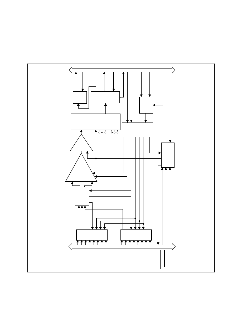
The AT-MIO-16 handles 16 channels of analog input with software-programmable gain and
12-bit A/D conversion. You change the position of jumpers to change the input mode, range,
and polarity. Figure 2-3 shows a block diagram of the analog input and data acquisition
circuitry.
GAIN1
GAIN0
Programmable
Gain Amplifier
Mux
1
Mux
0
ACH0
ACH1
ACH2
ACH3
ACH4
ACH5
ACH6
ACH7
ACH8
ACH9
ACH10
ACH1
1
ACH12
ACH13
ACH14
ACH15
SCANCLK
Start T
rigger
External Convert
Stop T
rigger
CONVERT
LAST
ONE
MA3
MA2
MA1
MA0
Counter/T
imer
Signals
MUXCTRCLK
/
4
/
4
Data
MUXCTR
WR
/
6
Data
MUXGAINWR
CONV
A
V
AIL
A/D RD
/
12
Data
/
12
A/D
Data
Sign
Exten-
sion
A/D RD
/
4
Data
+
–
10 V/20 V
Selection
(W1)
MUX0OUT
MUX0EN
MUX1OUT
MUX1EN
AISENSE
SCANCLK
ST
OPTRIG
EXTCONV
ST
AR
TTRIG
S/H
Ampli-
fier
Unipolar/Bipolar
Selection (W4)
PC A
T I/O Channel
I/O Connector
ADC
A/D
FIFO
Mux
Counter
Mux
Gain
Memory
Data
Acquisition
T
iming
Mux Mode
Selection
(W6 &
W9)
Figure 2-3. Analog Input and Data Acquisition Circuitry Block Diagram
Chapter 2
Configuration and Installation
© National Instruments Corporation
2-9
AT-MIO-16 User Manual
Input Mode
The AT-MIO-16 has three different input modes—differential (DIFF) input, referenced single-
ended (RSE) input, and nonreferenced single-ended (NRSE) input. The single-ended input
configurations use 16 channels. The DIFF input configuration uses eight channels. You may
find it helpful to refer to the Analog Input Signal Connections section in Chapter 3, Signal
Connections, which contains diagrams showing the signal paths for the three configurations.
The multiplexer-mode selection jumpers configure the analog input channels as 16 single-ended
inputs or 8 differential inputs. When single-ended mode is selected, the outputs of the two
multiplexers are tied together and routed to the positive (+) input of the instrumentation
amplifier. The negative (-) input of the instrumentation amplifier is tied to the AT-MIO-16
ground for RSE input or to the analog return of the input signals via the AI SENSE input on the
I/O connector for NRSE input. When DIFF mode is selected, the output of MUX0 is routed to
the positive (+) input of the instrumentation amplifier, and the output of MUX1 is routed to the
negative (-) input of the instrumentation amplifier.
DIFF Input (Eight Channels, Factory Setting).
DIFF input means that each input signal has its own reference, and the difference between each
signal and its reference is measured. The signal and its reference are each assigned an input
channel. With this input configuration, the AT-MIO-16 can monitor eight different analog input
signals. You select the DIFF input configuration by setting jumpers W6 and W9 shown in
Table 2-6.
Table 2-6. DIFF Input Configuration (Factory Setting)
Jumper
Settings
Description
W6
H
F
D
B
G
E
C
A
Jumper is placed in standby position or can be discarded.
AISENSE is tied to the instrumentation amplifier output ground point.
Channels 0 through 7 are tied to the positive input of the instrumentation
amplifier. Channels 8 through 15 are tied to the negative input of the
instrumentation amplifier.
W9
DIFF
SE
•
The multiplexer is configured to control eight input channels.
RSE Input (16 Channels).
RSE input means that all input signals are referenced to a common ground point that is also tied
to the analog input ground of the AT-MIO-16 board. The negative input of the differential input
amplifier is tied to the analog ground. This configuration is useful when measuring floating
signal sources. See the Types of Signal Sources section in Chapter 3, Signal Connections, for
more information. With this input configuration, the AT-MIO-16 can monitor 16 different
analog input signals. You select the RSE input configuration by setting jumpers W6 and W9 as
shown in Table 2-7.
Configuration and Installation
Chapter 2
AT-MIO-16 User Manual
2-10
© National Instruments Corporation
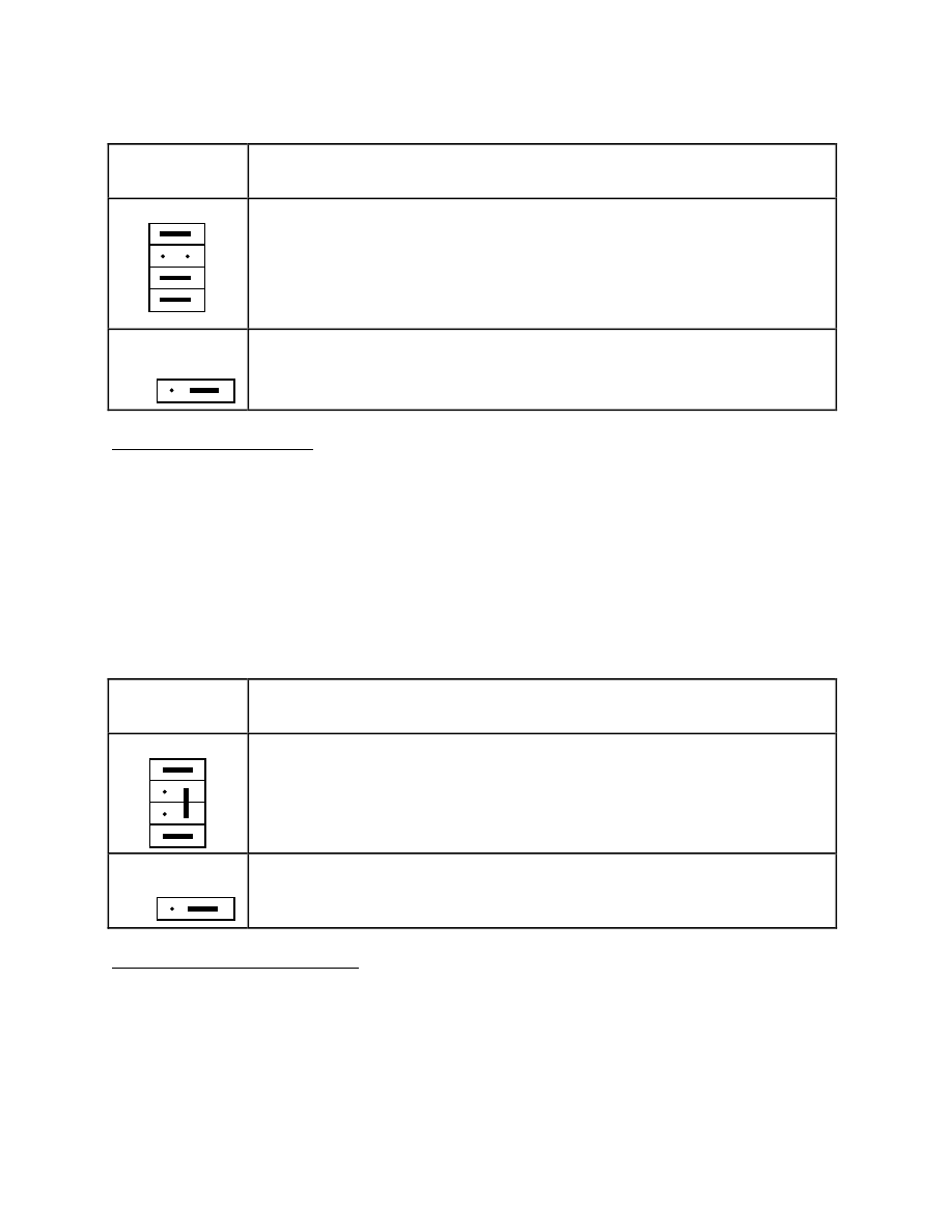
Table 2-7. RSE Input Configuration
Jumper
Settings
Description
W6
H
F
D
B
G
E
C
A
AISENSE is tied to the instrumentation amplifier signal ground.
The instrumentation amplifier negative input is tied to the instrumentation
amplifier signal ground.
The multiplexer outputs are tied together into the positive input of the
instrumentation amplifier.
W9
DIFF
SE
The multiplexer is configured to control 16 input channels.
NRSE Input (16 Channels).
NRSE input means that all input signals are referenced to the same common mode voltage, but
that this common mode voltage is allowed to float with respect to the analog ground of the
AT-MIO-16 board. This common mode voltage is subsequently subtracted out by the input
instrumentation amplifier. This configuration is useful when measuring ground-referenced
signal sources. See the Types of Signal Sources section in Chapter 3, Signal Connections, for
more information. With this input configuration, the AT-MIO-16 can measure 16 different
analog input signals. You select the NRSE input configuration by setting jumpers W6 and W9 as
shown in Table 2-8.
Table 2-8. NRSE Input Configuration
Jumper
Settings
Description
W6
H
F
D
B
G
E
C
A
AISENSE is tied to the negative input of the instrumentation amplifier.
The jumper is placed in standby position or can be discarded.
The multiplexer outputs are tied together into the positive input of the
instrumentation amplifier.
W9
DIFF
SE
The multiplexer control is configured to control 16 input channels.
Analog Input Polarity and Range
The AT-MIO-16 has two input polarities—unipolar and bipolar. Unipolar input means that the
input voltage range is between 0 and V
ref
where V
ref
is some positive reference voltage. Bipolar
input means that the input voltage range is between -V
ref
and +V
ref
. The AT-MIO-16 also has
two input ranges—a 10 V input range and a 20 V input range. You can select one of three
possible input polarity and range configurations as shown in Table 2-9.
Chapter 2
Configuration and Installation
© National Instruments Corporation
2-11
AT-MIO-16 User Manual
Table 2-9. Configurations for Input Range and Input Polarity
Input Polarity Jumper
Settings
Input Range
Jumper Settings
Bipolar
(factory setting)
W4
U
B
ADC Mode
-10 to +10 V (20 V range)
(factory setting)
W1
20 V
10 V
ADC Range
-5 to +5 V (10 V range)
W1
20 V
10 V
ADC Range
Unipolar
W4
U
B
ADC Mode
0 to +10 V (10 V range)
W1
20 V
10 V
ADC Range
Sign-extension circuitry at the ADC FIFO output adds four most significant bits (MSBs), bits 15
through 12, to the 12-bit FIFO output (bits 11 through 0) to produce a 16-bit result. The sign-
extension circuitry is software programmable to generate either straight binary numbers or two's
complement numbers. In straight binary mode, bits 15 through 12 are always zero and provide a
range of 0 to 4,095. In two's complement mode, the MSB of the 12-bit ADC result, bit 11, is
inverted and extended to bits 15 through 12, providing a range of -2,048 to +2,047.
Considerations for Selecting Input Ranges.
Input polarity/range selection depends on the expected input range of the incoming signal. A
large input range can accommodate a large signal variation but sacrifices voltage resolution.
Choosing a smaller input range increases voltage resolution but may cause the input signal to go
out of range. For best results, match the input range as closely as possible to the expected range
of the input signal. For example, if the input signal will never become negative (below 0 V), a
unipolar input is best. However, if the signal does become negative, inaccurate readings will
occur.
The AT-MIO-16 software-programmable gain increases its overall flexibility by matching input
signal ranges to those the AT-MIO-16 ADC accommodates. The AT-MIO-16H board has gains
of 1, 2, 4, and 8 and is suited for high-level signals near the range of the ADC. The
AT-MIO-16L board is designed to measure low-level signals and has gains of 1, 10, 100,
and 500. With the proper gain setting, you can use the full resolution of the ADC to measure the
input signal. Table 2-10 shows the overall input range and precision according to the input range

Configuration and Installation
Chapter 2
AT-MIO-16 User Manual
2-12
© National Instruments Corporation
configuration and gain used. In single-channel data acquisition applications, the maximum
allowable rate is 100 kHz, or the maximum specified rate of the AT-MIO-16 board.
Multichannel applications may need to slow the acquisition rate due to gain. These numbers are
listed in Table 2-10 as well.
Table 2-10. Actual Range and Measurement Precision
Versus Input Range Selection and Gain
Range
Configuration
Board
Model
Gain
Actual Input
Range
Precision
Maximum
Multichannel
Acquisition Rate
0 to +10 V
1
0 to +10 V
2.44 mV
100 kHz
-H
2
0 to +5 V
1.22 mV
100 kHz
4
0 to +2.5 V
610
µ
V
100 kHz
8
0 to +1.25 V
305
µ
V
100 kHz
1
0 to +10 V
2.44 mV
100 kHz
-L
10
0 to +1 V
244
µ
V
100 kHz
100
0 to +0.1 V
24.4
µ
V
70 kHz
500
0 mV to +20 mV
4.88
µ
V
20 kHz
-5 to +5 V
1
-5 to +5 V
2.44 mV
100 kHz
-H
2
-2.5 to +2.5 V
1.22 mV
100 kHz
4
-1.25 to +1.25 V
610
µ
V
100 kHz
8
-0.625 to +0.625 V
305
µ
V
100 kHz
1
-5 to +5 V
2.44 mV
100 kHz
-L
10
-0.5 to +0.5 V
244
µ
V
100 kHz
100
-50 mV to +50 mV
24.4
µ
V
70 kHz
500
-10 mV to +10 mV
4.88
µ
V
20 kHz
-10 to +10 V
1
-10 to +10 V
4.88 mV
100 kHz
-H
2
-5 to +5 V
2.44 mV
100 kHz
4
-2.5 to +2.5 V
1.22 mV
100 kHz
8
-1.25 to +1.25 V
610
µ
V
100 kHz
1
-10 to +10 V
4.88 mV
100 kHz
-L
10
-1 to +1 V
488
µ
V
100 kHz
100
-0.1 to +0.1 V
48.8
µ
V
70 kHz
500
-20 mV to +20 mV
9.76
µ
V
20 kHz
*
The value of 1 LSB of the 12-bit ADC, that is, the voltage increment corresponding to a change of 1 count
in the ADC 12-bit count.
Analog Output Configuration
The AT-MIO-16 provides two channels of 12-bit digital-to-analog (D/A) output. Each analog
output channel provides options such as unipolar or bipolar output and internal or external
reference voltage selection. Figure 2-4 shows a block diagram of the analog output circuitry.
Chapter 2
Configuration and Installation
© National Instruments Corporation
2-13
AT-MIO-16 User Manual
I/O Connector
REF
Selection
(W3)
+10 V
(From
A/D
REF)
Internal
REF
EXTREF
(W2)
(W7)
REF
DAC1 + op-amps
DAC1WR
DATA
/
12
DAC0OUT
(W8)
AOGND
DAC1OUT
DAC0 + op-amps
DAC0WR
PC
A
T
I/O Channel
Bipolar/
Unipolar
Selection
Bipolar/
Unipolar
Selection
Figure 2-4. Analog Output Circuitry Block Diagram
Analog Output Reference
You can connect each DAC to the AT-MIO-16 internal reference of 10 V or to the external
reference signal connected to the EXTREF pin on the I/O connector. This signal applied to
EXTREF must be between -10 V and +10 V. Both channels need not be configured the same
way. When you select the external reference jumper setting, the voltage at EXTREF on the I/O
connector is connected to the DAC reference input. When you select the internal reference
jumper setting, the onboard 10 V reference signal is connected to the DAC reference input.
You select the external or internal reference signal for each analog output channel by setting
jumpers W2 and W3 as shown in Table 2-11.
Configuration and Installation
Chapter 2
AT-MIO-16 User Manual
2-14
© National Instruments Corporation
Table 2-11. Internal and External Reference Selection
Analog Output
Jumper Settings
Channel
Internal (Factory Setting)
External
0
W3
EXT
INT
DAC0
W2
EXT
INT
DAC0
1
W3
EXT
INT
DAC1
W2
EXT
INT
DAC1
Analog Output Polarity Selection
You can configure each analog output channel for either unipolar or bipolar output. A unipolar
configuration has a range of 0 to V
ref
at the analog output. A bipolar configuration has a range
of -V
ref
to +V
ref
at the analog output. V
ref
is the voltage reference the DACs use in the analog
output circuitry and can either be the 10 V onboard reference or an externally supplied reference
between -10 V and +10 V. Both channels need not be configured the same way; however, at the
factory both channels are configured for bipolar output.
Analog Output Data Coding.
You must select whether to write to the DAC in straight binary format or two's complement
format. In two's complement mode, data values written to the analog output channel range from
-2,048 to +2,047 decimal (F800 to 07FF hex). In straight binary mode, data values written to the
analog output channel range from 0 to 4,095 decimal (0 to 0FFF hex). Two’s complement
coding is best suited to the bipolar analog output mode, which is the AT-MIO-16 factory setting.
Straight binary coding is usually used for the unipolar analog output configuration.
The analog output polarity and data mode configurations are shown in Table 2-12. Table 2-13
shows the relationship of the output range to the polarity.
Chapter 2
Configuration and Installation
© National Instruments Corporation
2-15
AT-MIO-16 User Manual
Table 2-12. Analog Output Polarity and Data Mode Configuration
Analog
Output
Channel
Polarity
Jumper
Settings
Data
Mode
Jumper
Settings
0
Bipolar
(factory setting)
W8
B
U
DAC0
Two’s
complement
(factory setting)
W10
2SC
BIN
DAC0
Unipolar
W8
B
U
DAC0
Straight binary
W10
2SC
BIN
DAC0
1
Bipolar
(factory setting)
W7
B
U
DAC1
Two’s
complement
(factory setting)
W11
2SC
BIN
DAC1
Unipolar
W7
DAC1
B
U
Straight binary
W11
2SC
BIN
DAC1
Table 2-13. Output Range Selection and Precision
Polarity
Output Range
Precision
Unipolar
0 - 10 V
2.44 mV
Bipolar
-10 - +10 V
4.88 mV
Note: If you are using software such as LabVIEW, LabWindows, or NI-DAQ, you may need
to reconfigure your software to reflect any changes in jumper or switch settings.
Digital I/O Configuration
The AT-MIO-16 provides eight digital I/O lines. These lines are divided into two ports of four
lines each and are located at pins ADIO<3..0> and BDIO<3..0> on the I/O connector. You can
configure each port for input or output through software programming of a register on the
AT-MIO-16 board. Figure 2-5 shows a block diagram of the digital I/O circuitry.
Configuration and Installation
Chapter 2
AT-MIO-16 User Manual
2-16
© National Instruments Corporation
I/O Connector
A
Digital
Input
Register
B
EXTSTROBEWR*
EXTSTROBE*
/
4
/
4
/
4
/
4
DOREGWR
DOUT0 ENABLE
/
4
DATA <3..0>
DATA <7..4>
/
4
DOUT1 ENABLE
DIREGRD
DATA <7..0>
/
8
BDIO <3..0>
ADIO <3..0>
PC
A
T
I/O Channel
DOUT1
Digital
Output
Register
DOUT0
Digital
Output
Register
Figure 2-5. Digital I/O Circuitry Block Diagram
The Digital Output Register controls the digital I/O lines and the Digital Input Register monitors
them. The Digital Output Register is an 8-bit register that contains the digital output values for
both ports 0 and 1. When port 0 is enabled, bits <3..0> in the Digital Output Register are driven
onto digital output lines ADIO<3..0>. When port 1 is enabled, bits <7..4> in the Digital Output
Register are driven onto digital output lines BDIO<3..0>.
Reading the Digital Input Register returns the state of the digital I/O lines. Digital I/O lines
ADIO<3..0> are connected to bits <3..0> of the Digital Input Register. Digital I/O lines
BDIO<3..0> are connected to bits <7..4> of the Digital Input Register. When a port is enabled,
the Digital Input Register serves as a read-back register, returning the digital output value of the
port. When a port is not enabled, reading the Digital Input Register returns the state of the digital
I/O lines as driven by an external device.
Chapter 2
Configuration and Installation
© National Instruments Corporation
2-17
AT-MIO-16 User Manual
RTSI Bus Clock Selection
When multiple AT Series boards are connected via the RTSI bus, you may want all the boards to
use the same 10 MHz clock. This arrangement is useful for applications that require
counter/timer synchronization between boards. Each AT Series board with a RTSI bus interface
has an onboard 10 MHz oscillator. Thus, one board can drive the RTSI bus clock signal, and the
other boards can receive this signal or disconnect from it.
The configuration for jumper W5 specifies whether a board is to drive the onboard 10 MHz
oscillator onto the RTSI bus, receive the RTSI bus clock, or disconnect from the RTSI bus clock.
This clock source, whether local or RTSI signal, is then divided by 10 and used as the Am9513A
frequency source. The jumper selections are shown in Table 2-14.
Table 2-14. Configurations for RTSI Bus Clock Selection
Local Clock
Slave Clock
Master Clock
Use the local oscillator as
the board clock (factory
setting)
Receive the RTSI bus clock
signal
Drive the RTSI bus clock
and the board clock signal
with the local oscillator
W5
BRD
BRD
NC
R
TSI
10 MHz
NC
W5
BRD
BRD
NC
R
TSI
10 MHz
NC
W5
BRD
BRD
NC
R
TSI
10 MHz
NC
Hardware Installation
You can install the AT-MIO-16 in any available 16-bit expansion slot (AT style) in your
computer. The AT-MIO-16 does not work if installed in an eight-bit expansion slot (PC style).
After you have changed (if needed), verified, and recorded the switches and jumper settings, you
are ready to install the AT-MIO-16. The following are general installation instructions, but
consult your PC AT user manual or technical reference manual for specific instructions and
warnings.
1. Turn off your computer.
2. Remove the top cover or access port to the I/O channel.
3. Remove the expansion slot cover on the back panel of the computer.

Configuration and Installation
Chapter 2
AT-MIO-16 User Manual
2-18
© National Instruments Corporation
4. Write down your hardware configuration settings in the AT-MIO-16 Hardware and Software
Configuration Form in Appendix C at the back of this manual. You will need these settings
when you install and configure your software.
5. Insert the AT-MIO-16 into a 16-bit slot. It may be a tight fit, but do not force the board into
place.
6. Screw the mounting bracket of the AT-MIO-16 to the back panel rail of the computer.
7. Check the installation.
8. Replace the cover.
The AT-MIO-16 board is installed. You are now ready to install and configure your software.
If you are using NI-DAQ, refer to the NI-DAQ Software Reference Manual for PC Compatibles.
The software installation and configuration instructions are in Chapter 1, Introduction to
NI-DAQ. Find the installation and system configuration section for your operating system and
follow the instructions given there.
If you are using LabVIEW, the software installation instructions are in your LabVIEW release
notes. After you have installed LabVIEW, refer to the Configuring LabVIEW section of
Chapter 1 in your LabVIEW user manual for software configuration instructions.
If you are using LabWindows, the software installation instructions are in Part 1, Introduction to
LabWindows, of the Getting Started with LabWindows manual. After you have installed
LabWindows, refer to Chapter 1, Configuring LabWindows, of the LabWindows User Manual
for software configuration instructions.

© National Instruments Corporation
3-1
AT-MIO-16 User Manual
Chapter 3
Signal Connections
This chapter describes the signal connections to the AT-MIO-16 board, and cable wiring.
I/O Connector
Figure 3-1 shows the pin assignments for the AT-MIO-16 I/O connector. This connector is
located on the back panel of the AT-MIO-16 board and is accessible at the rear of the computer
after the board has been properly installed.
Warning:
Connections that exceed any of the maximum ratings of input or output signals
on the AT-MIO-16 can damage the AT-MIO-16 board and the PC AT. The
description of each signal in this section includes information about maximum
input ratings. National Instruments is not liable for any damages resulting from
incorrect signal connections.
Signal Connections
Chapter 3
AT-MIO-16 User Manual
3-2
© National Instruments Corporation
1
50
49
48
47
46
45
44
43
42
41
40
39
38
37
36
35
34
33
32
31
30
29
28
27
26
25
24
23
22
21
20
19
18
17
16
15
14
13
12
11
10
9
8
7
6
5
4
3
2
BDIO0
DIGGND
AIGND
ACH0
ACH1
ACH2
ACH3
ACH4
ACH5
ACH6
ACH7
AISENSE
ADIO0
ADIO1
ADIO2
DIGGND
STOPTRIG
OUT1
GATE5
AIGND
ACH8
ACH9
AOGND
ADIO3
+5 V
GATE2
OUT5
EXTREF
BDIO3
+5 V
GATE1
OUT2
FOUT
EXTSTROBE*
DAC1OUT
SOURCE1
SOURCE5
ACH10
ACH11
ACH12
ACH13
ACH14
ACH15
DAC0OUT
BDIO1
SCANCLK
STARTRIG*
EXTCONV*
SOURCE2
BDIO2
Figure 3-1. AT-MIO-16 I/O Connector Pin Assignments

Chapter 3
Signal Connections
© National Instruments Corporation
3-3
AT-MIO-16 User Manual
Signal Descriptions
Pin
Signal Name
Reference
Description
1, 2
AIGND
N/A
Analog Input Ground—These pins are the reference point for
single-ended measurements and the bias current return point
for differential measurements.
3–18
ACH<0..15>
AIGND
Analog Input Channels 0 through 15—In the DIFF mode, the
input is configured for up to 8 channels. In single-ended
mode, the input is configured for up to 16 channels.
19
AISENSE
AIGND
Analog Input Sense—This pin serves as the reference node
when the board is in NRSE configuration. If desired, this
signal can be programmed to be driven by the board analog
input ground.
20
DAC0OUT
AOGND
Analog Channel 0 Output—This pin supplies the voltage
output of analog output channel 0.
21
DAC1OUT
AOGND
Analog Channel 1 Output—This pin supplies the voltage
output of analog output channel 1.
22
EXTREF
AOGND
External Reference—This is the external reference input for
the analog output circuitry.
23
AOGND
N/A
Analog Output Ground—The analog output voltages are
referenced to this node.
24, 33
DIGGND
N/A
Digital Ground—This pin supplies the reference for the digital
signals at the I/O connector as well as the +5 VDC supply.
25, 27,
29, 31
ADIO<0..3>
DIGGND
Digital I/O port A signals.
26, 28,
30, 32
BDIO<0..3>
DIGGND
Digital I/O port B signals.
34, 35
+5 V
DIGGND
+5 VDC Source—This pin is fused for up to 1 A of +5 V
supply.
36
SCANCLK
DIGGND
Scan Clock—This pin pulses once for each A/D conversion in
the scanning modes. The low-to-high edge indicates when the
input signal can be removed from the input or switched to
another signal.
37
EXTSTROBE*
DIGGND
External Strobe—Writing to the EXTSTROBE* Register
results in a minimum 200 ns low pulse on this pin.
38
STARTTRIG*
DIGGND
External Trigger—In posttrigger data acquisition sequences, a
high-to-low edge on STARTTRIG* initiates the sequence. In
pretrigger applications, the high-to-low edge of STARTTRIG*
initiates pretrigger conversions while the STOPTRIG signal
initiates the posttrigger sequence.
39
STOPTRIG
DIGGND
Stop Trigger—In pretrigger data acquisition, the low-to-high
edge of STOPTRIG initiates the posttrigger sequence.
40
EXTCONV*
DIGGND
External Convert—A high-to-low edge on EXTCONV* causes
an A/D conversion to occur. If EXTGATE* or EXTCONV*
is low, conversions are inhibited.
41
SOURCE1
DIGGND
SOURCE1—This pin is from the Am9513A Counter 1 signal.
42
GATE1
DIGGND
GATE1—This pin is from the Am9513A Counter 1 signal.
(continues)

Signal Connections
Chapter 3
AT-MIO-16 User Manual
3-4
© National Instruments Corporation
Pin
Signal Name
Reference
Description (Continued)
43
OUT1
DIGGND
OUTPUT1—This pin is from the Am9513A Counter 1 signal.
44
SOURCE2
DIGGND
SOURCE2—This pin is from the Am9513A Counter 2 signal.
45
GATE2
DIGGND
GATE2—This pin is from the Am9513A Counter 2 signal.
46
OUT2
DIGGND
OUT2—This pin is from the Am9513A Counter 2 signal.
47
SOURCE5
DIGGND
SOURCE5—This pin is from the Am9513A Counter 5 signal.
48
GATE5
DIGGND
GATE5—This pin is from the Am9513A Counter 5 signal.
49
OUT5
DIGGND
OUT5—This pin is from the Am9513A Counter 5 signal.
50
FOUT
DIGGND
FOUT—This pin is from the Am9513A FOUT signal.
The signals on the connector can be grouped into analog input signals, analog output signals,
digital I/O signals, digital power connections, or timing I/O signals. Signal connection
guidelines for each of these groups are described in the following sections.
Analog Input Signal Connections
Pins 1 through 19 of the I/O connector are analog input signal pins. Pins 1 and 2 are AIGND
signal pins. AIGND is an analog input common signal that is routed directly to the ground tie
point on the AT-MIO-16. You can use these pins for a general analog power ground tie point to
the AT-MIO-16 if necessary. Pin 19 is the AISENSE pin. In single-ended mode, this pin is
connected internally to the negative input of the AT-MIO-16 instrumentation amplifier. In DIFF
mode, this signal is connected to the reference ground at the output of the instrumentation
amplifier.
Pins 3 through 18 are the ACH<15..0> signal pins. These pins are tied to the 16 analog input
channels of the AT-MIO-16. In single-ended mode, signals connected to ACH<15..0> are routed
to the positive input of the AT-MIO-16 instrumentation amplifier. In DIFF mode, signals
connected to ACH<7..0> are routed to the positive input of the AT-MIO-16 instrumentation
amplifier, and signals connected to ACH<15..8> are routed to the negative input of the
AT-MIO-16 instrumentation amplifier.
The following input ranges and maximum ratings apply to inputs ACH<15..0>:
•
Differential input range
±
10 V
•
Common-mode input range
±
7 V with respect to AT-MIO-16 AIGND
•
Input range
±
12 V with respect to AT-MIO-16 AIGND
•
Maximum input voltage rating
±
20 V for the AT-MIO-16 board powered off
±
35 V for the AT-MIO-16 board powered on
Warning:
Exceeding the differential and common-mode input ranges results in distorted
input signals. Exceeding the maximum input voltage rating may damage the
AT-MIO-16 board and the PC AT. National Instruments is not liable for any
damages resulting from incorrect signal connections.
Chapter 3
Signal Connections
© National Instruments Corporation
3-5
AT-MIO-16 User Manual
Connection of analog input signals to the AT-MIO-16 depends on the configuration of the
AT-MIO-16 analog input circuitry and the type of input signal source. The different AT-MIO-16
configurations use the AT-MIO-16 instrumentation amplifier in different ways. Figure 3-2
shows a diagram of the AT-MIO-16 instrumentation amplifier.
-
Instrumentation
Amplifier
-
Measured
Voltage
V
m
= [V
in
+ -V
in
-] * Gain
V
in
-
V
m
V
in
+
+
+
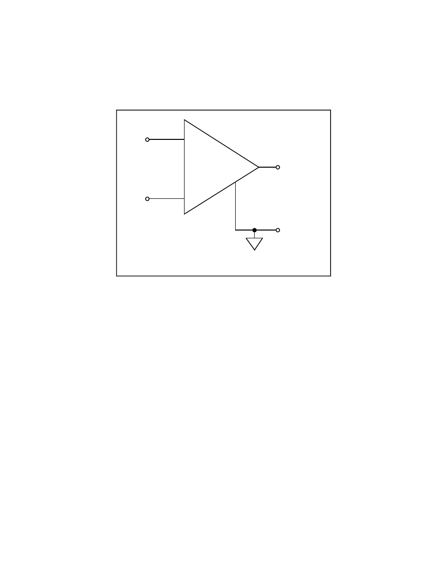
Figure 3-2. AT-MIO-16 Instrumentation Amplifier
The AT-MIO-16 instrumentation amplifier applies gain, common-mode voltage rejection, and
high-input impedance to the analog input signals connected to the AT-MIO-16 board. Signals
are routed to the positive and negative inputs of the instrumentation amplifier through input
multiplexers on the AT-MIO-16. The instrumentation amplifier converts two input signals to a
signal that is the difference between the two input signals multiplied by the gain setting of the
amplifier. The amplifier output voltage is referenced to the AT-MIO-16 ground. The
AT-MIO-16 ADC measures this output voltage when it performs A/D conversions.
All signals must be referenced to ground somewhere, either at the source device or at the
AT-MIO-16. If you have a floating source, you must use a ground-referenced input connection
at the AT-MIO-16. If you have a grounded source, you must use a nonreferenced input
connection at the AT-MIO-16.
Types of Signal Sources
When configuring the input mode of the AT-MIO-16 and making signal connections, you must
first determine whether the signal source is floating or ground referenced. These two types of
signals are described in the following sections.

Signal Connections
Chapter 3
AT-MIO-16 User Manual
3-6
© National Instruments Corporation
Floating Signal Sources
A floating signal source is one that is not connected in any way to the building ground system
but rather has an isolated ground-reference point. Some examples of floating signal sources are
outputs of transformers, thermocouples, battery-powered devices, optical isolator outputs, and
isolation amplifiers. The ground reference of a floating signal must be tied to the AT-MIO-16
analog input ground to establish a local or onboard reference for the signal. Otherwise, the
measured input signal varies or appears to float. An instrument or device that provides an
isolated output falls into the floating signal source category.
Ground-Referenced Signal Sources
A ground-referenced signal source is one that is connected in some way to the building system
ground and is therefore already connected to a common ground point with respect to the
AT-MIO-16 board, assuming that the PC AT is plugged into the same power system.
Nonisolated outputs of instruments and devices that plug into the building power system fall into
this category.
The difference in ground potential between two instruments connected to the same building
power system is typically between 1 mV and 100 mV, but can be much higher if power
distribution circuits are not properly connected. If grounded signal source is measured
improperly, this difference may show up as an error in the measurement. The following
connection instructions for grounded signal sources should eliminate this ground potential
difference from the measured signal.
Input Configurations
You can configure the AT-MIO-16 for one of three input modes—NRSE, RSE, or DIFF. The
following sections discuss the use of single-ended and differential measurements, and
considerations for measuring both floating and ground-referenced signal sources. Table 3-1
summarizes the recommended input configuration for both types of signal sources.
Table 3-1. Recommended Input Configurations for Ground-Referenced
and Floating Signal Sources
Type of Signal
Recommended Input
Configuration
Ground-Referenced
(nonisolated outputs,
plug-in instruments)
DIFF
NRSE
Floating
(batteries, thermocouples,
isolated outputs)
DIFF with bias resistors
RSE

Chapter 3
Signal Connections
© National Instruments Corporation
3-7
AT-MIO-16 User Manual
Differential Connection Considerations (DIFF Configuration)
Differential connections are those in which each AT-MIO-16 analog input signal has its own
reference signal or signal return path. These connections are available when the AT-MIO-16 is
configured in the DIFF mode. Each input signal is tied to the positive input of the
instrumentation amplifier. The reference signal, or return, is tied to the negative input of the
instrumentation amplifier.
When the AT-MIO-16 is configured for DIFF input, each signal uses two of the multiplexer
inputs–one for the signal and one for its reference signal. Therefore, only eight analog input
channels are available when using the DIFF configuration. Use the DIFF input configuration
when any of the following conditions are present:
•
Input signals are low level (less than 1 V).
•
Leads connecting the signals to the AT-MIO-16 are greater than 15 ft.
•
Any of the input signals requires a separate ground-reference point or return signal.
•
The signal leads travel through noisy environments.
Differential signal connections reduce picked-up noise, increase common-mode signal and noise
rejection, and cause input signals to float within the common-mode limits of the input
instrumentation amplifier.
Signal Connections
Chapter 3
AT-MIO-16 User Manual
3-8
© National Instruments Corporation
Differential Connections for Grounded Signal Sources
Figure 3-3 shows how to connect a ground-referenced signal source to an AT-MIO-16 board
configured for DIFF input. Configuration instructions are included in the Analog Input
Configuration section of Chapter 2, Configuration and Installation.
Ground-
Referenced
Signal
Source
Common
Mode
Noise,
Ground
Potential,
and so on
Input Multiplexers
AISENSE
Instrumentation
Amplifier
Vm
Measured
Voltage
AIGND
-
+
-
+
Vs
V
cm
+
-
-
+
I/O Connector
AT-MIO-16 Board in DIFF Configuration
3
5
7
17
4
6
8
18
19
1, 2
ACH<0..7>
ACH<8..15>
Figure 3-3. Differential Input Connections for Grounded Signal Sources
With this type of connection, the instrumentation amplifier rejects both the common-mode noise
in the signal and the ground-potential difference between the signal source and the AT-MIO-16
ground (shown as V
cm
in Figure 3-3).
Differential Connections for Floating Signal Sources
Figure 3-4 shows how to connect a floating signal source to an AT-MIO-16 board configured for
DIFF input. Configuration instructions are included in the Analog Input Configuration section of
Chapter 2, Configuration and Installation.
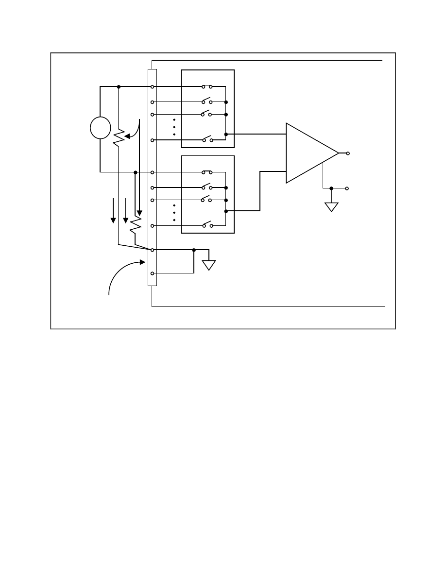
Chapter 3
Signal Connections
© National Instruments Corporation
3-9
AT-MIO-16 User Manual
+
-
+
Floating
Signal
Source
Input Multiplexers
Instrumentation
Amplifier
V
m
Measured
Voltage
-
V
S
-
+
I/O Connector
AT-MIO-16 Board in DIFF Configuration
3
5
7
17
4
6
8
18
AIGND
1, 2
100 k
Ω
Bias
Current
Return
Paths
ACH<8..15>
ACH<0..7>
19
AISENSE
Figure 3-4. Differential Input Connections for Floating Signal Sources
The 100 k
Ω
resistors shown in Figure 3-4 create a return path to ground for the bias currents of
the instrumentation amplifier. If there is no return path, the instrumentation amplifier bias
currents charge up stray capacitances, resulting in uncontrollable drift and possible saturation in
the amplifier. Typically, resistors from 10 k
Ω
to 100 k
Ω
are used.
A resistor from each input to ground, as shown in Figure 3-4, produces bias current return paths
for an AC-coupled input signal. This solution, although necessary for AC-coupled signals,
lowers the input impedance of the analog input channel. In addition, the input offset current of
the instrumentation amplifier contributes a DC offset voltage at the input. The amplifier has a
maximum input offset current of
±
15 nA and a typical offset current drift of
±
20 pA/
°
C.
Multiplied by the 100 k
Ω
resistor, this current contributes a maximum offset voltage of 1.5 mV
and a typical offset voltage drift of 2
µ
V/
°
C at the input. Keep this in mind when you observe
DC offsets with AC-coupled inputs.
If the input signal is DC-coupled, you need only the resistor that connects the negative signal
input to ground. This connection does not lower the input impedance of the analog input
channel.
Signal Connections
Chapter 3
AT-MIO-16 User Manual
3-10
© National Instruments Corporation
Single-Ended Connection Considerations
Single-ended connections are those in which all AT-MIO-16 analog input signals are referenced
to one common ground. The input signals are tied to the positive input of the instrumentation
amplifier, and their common ground point is tied to the negative input of the instrumentation
amplifier.
When the AT-MIO-16 is configured for single-ended input (NRSE or RSE), 16 analog input
channels are available. You can use single-ended input connections when the following criteria
are met by all input signals:
•
Input signals are high level (greater than 1 V).
•
Leads connecting the signals to the AT-MIO-16 are less than 15 ft.
•
All input signals share a common reference signal (at the source).
If any of the preceding criteria are not met, using DIFF input configuration is recommended.
You can jumper configure the AT-MIO-16 for two different types of single-ended connections—
RSE configuration and NRSE configuration. The RSE configuration is for floating signal
sources; in this case, the AT-MIO-16 produces the reference ground point for the external signal.
The NRSE configuration is for ground-referenced signal sources; in this case, the external signal
supplies its own reference ground point and the AT-MIO-16 should not supply one.
Single-Ended Connections for Floating Signal Sources (RSE Configuration)
Figure 3-5 shows how to connect a floating signal source to an AT-MIO-16 board configured for
single-ended input. You must configure the AT-MIO-16 analog input circuitry for RSE input to
make these types of connections. Configuration instructions are included in the Analog Input
Configuration section of Chapter 2, Configuration and Installation.
V
s
+
+
+
-
-
-
V
m
Measured
Voltage
Floating
Signal
Source
ACH<0..15>
Input Multiplexer
AIGND
Instrumentation
Amplifier
I/O Connector
3
5
7
18
1, 2
AT-MIO-16 Board in RSE Configuration
19
AISENSE
Figure 3-5. Single-Ended Input Connections for Floating Signal Sources
Chapter 3
Signal Connections
© National Instruments Corporation
3-11
AT-MIO-16 User Manual
Single-Ended Connections for Grounded Signal Sources (NRSE Configuration)
If you are measuring a grounded signal source with a single-ended configuration, you must
configure the AT-MIO-16 in the NRSE input configuration. Connect the signal to the positive
input of the AT-MIO-16 instrumentation amplifier and connect the signal local ground reference
to the negative input of the AT-MIO-16 instrumentation amplifier. Therefore, you must connect
the ground point of the signal to the AISENSE pin. Any potential difference between the
AT-MIO-16 ground and the signal ground appears as a common-mode signal at both the positive
and negative inputs of the instrumentation amplifier; the amplifier rejects this difference. On the
other hand, if the input circuitry of the AT-MIO-16 is referenced to ground, such as in the RSE
configuration, this difference in ground potentials appears as an error in the measured voltage.
Figure 3-6 shows how to connect a grounded signal source to an AT-MIO-16 board in the NRSE
configuration. Configuration instructions are included in the Analog Input Configuration section
of Chapter 2, Configuration and Installation.
V
s
+
+
+
-
-
-
V
m
Measured
Voltage
Ground-
Referenced
Signal
Source
ACH<0..15>
Input Multiplexer
AIGND
Instrumentation
Amplifier
I/O Connector
3
5
7
18
1, 2
AT-MIO-16 Board in NRSE Input Configuration
19
AISENSE
V
cm
+
-
Common-
Mode
Noise
and so on
Figure 3-6. Single-Ended Input Connections for Grounded Signal Sources
Common-Mode Signal Rejection Considerations
Figures 3-3 and 3-6 show connections for signal sources that are already referenced to some
ground point with respect to the AT-MIO-16. In these cases, the instrumentation amplifier can
reject any voltage caused by ground-potential differences between the signal source and the
AT-MIO-16. In addition, with differential input connections, the instrumentation amplifier can
reject common-mode noise pickup in the leads connecting the signal sources to the AT-MIO-16.

© National Instruments Corporation
3-12
AT-MIO-16 User Manual
The common-mode input range of the AT-MIO-16 instrumentation amplifier is defined as the
magnitude of the greatest common-mode signal that can be rejected.
The common-mode input range for the AT-MIO-16 depends on the size of the differential input
signal (V
diff
= V+
in
- V-
in
) and the gain setting of the instrumentation amplifier. The exact
formula for the allowed common-mode input range is as follows:
V
cm-max
=
±
(12 V -
V
diff
* Gain
2
)
where the maximum value for V
diff
is as follows:
±
10 V range
V
diff-max
=
±
10 V
0 to +10 V range
V
diff-max
= 10 V
±
5 V range
V
diff-max
=
±
5 V
For example, for a differential voltage as large as 20 mV and a gain of 500, the largest common-
mode voltage that can be rejected is
±
7 V. However, if the differential signal is 10 mV with a
gain of 500, a
±
9.5 V common-mode voltage can be rejected.
The common-mode voltage is measured with respect to the AT-MIO-16 ground and can be
calculated by the following formula:
V
cm-actual
=
V+
in
+ V-
in
2
where V+
in
is the signal at the positive input of the instrumentation amplifier and V-
in
is the
signal at the negative input of the instrumentation amplifier.
If the input signal common-mode range exceeds
±
7 V with respect to the AT-MIO-16 ground,
you must limit the amount of floating that occurs between the signal ground and the AT-MIO-16
ground.
Analog Output Signal Connections
Pins 20 through 23 of the I/O connector are analog output signal pins.
Pins 20 and 21 are the DAC0OUT and DAC1OUT signal pins. DAC0OUT is the voltage output
signal for analog output channel 0. DAC1OUT is the voltage output signal for analog output
channel 1.
Pin 22, EXTREF, is the external reference input for both analog output channels. You must
individually configure each analog output channel for external reference selection in order for the
signal applied at the external reference input to be used by that channel. Analog output
configuration instructions are included in the Analog Output Configuration section of Chapter 2,
Configuration and Installation.
The following ranges and ratings apply to the EXTREF input:
•
Useful input voltage range
±
10 V peak with respect to AOGND
•
Absolute maximum ratings
±
25 V peak with respect to AOGND
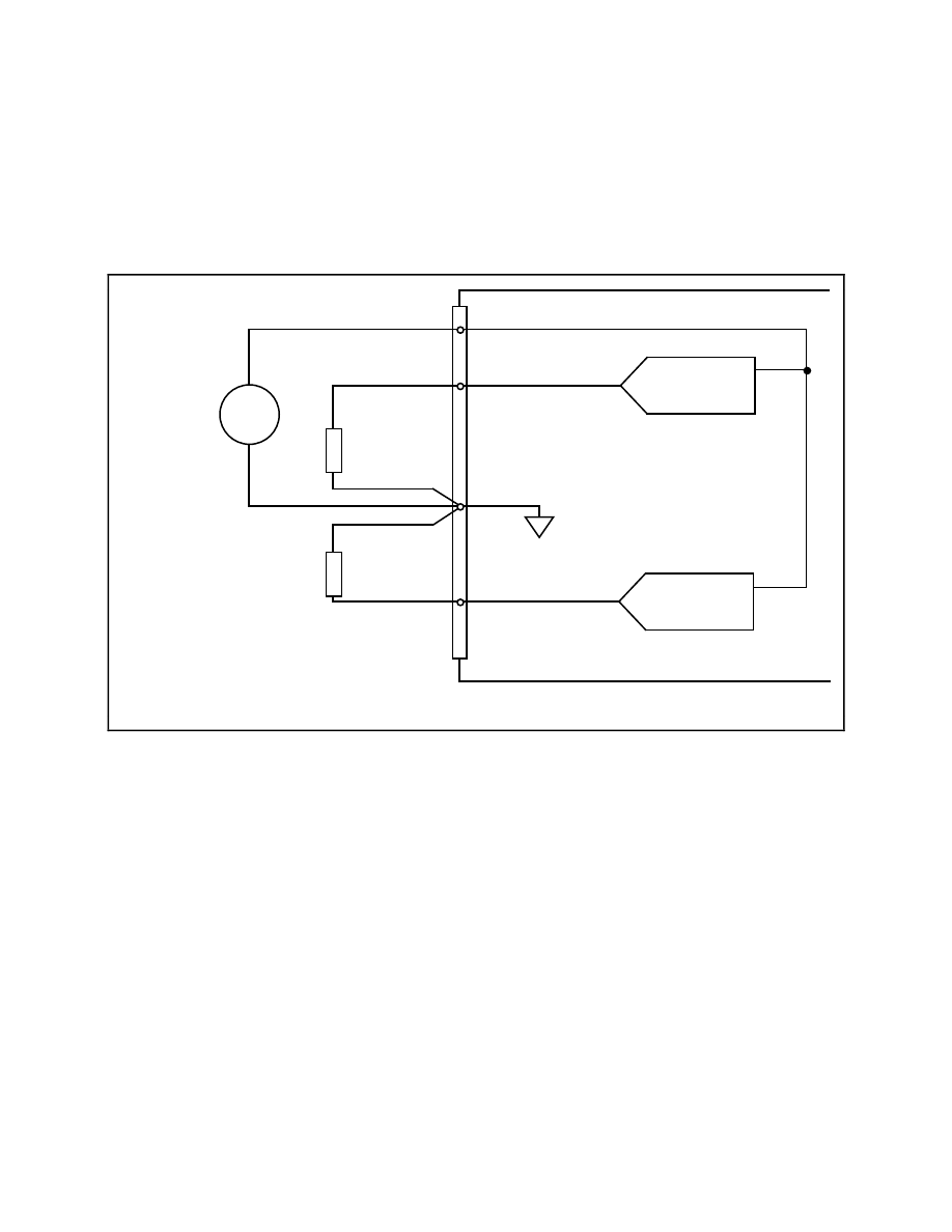
Chapter 3
Signal Connections
© National Instruments Corporation
3-13
AT-MIO-16 User Manual
Pin 23, AOGND, is the ground-reference point for both analog output channels and for the
external reference signal.
Figure 3-7 shows how to make analog output connections and the external reference input
connection to the AT-MIO-16 board. If neither channel is configured to use an external
reference signal, do not connect anything to the EXTREF pin.
+
-
+
-
+
-
V
ref
Channel 0
Channel 1
External
Reference
Signal
(Optional)
Load
Load
VOUT0
VOUT1
22
20
23
21
DAC1OUT
AOGND
DAC0OUT
EXTREF
Analog Output Channels
AT-MIO-16 Board
Figure 3-7. Analog Output Connections
The external reference signal can be either a DC or an AC signal. This reference signal is
multiplied by the DAC code to generate the output voltage. The DACs in the analog output
channels are rated for -82 dB THD with a 1 kHz, 6 Vrms sine wave reference signal and with the
DACs set at their maximum (full-scale) digital value.
Digital I/O Signal Connections
Pins 24 through 32 of the I/O connector are digital I/O signal pins.
Pins 25, 27, 29, and 31 are connected to the digital lines ADIO<3..0> for digital I/O port A. Pins
26, 28, 30, and 32 are connected to the digital lines BDIO<3..0> for digital I/O port B. Pin 24,
DIGGND, is the digital ground pin for both digital I/O ports. You can individually program
ports A and B to be inputs or outputs.
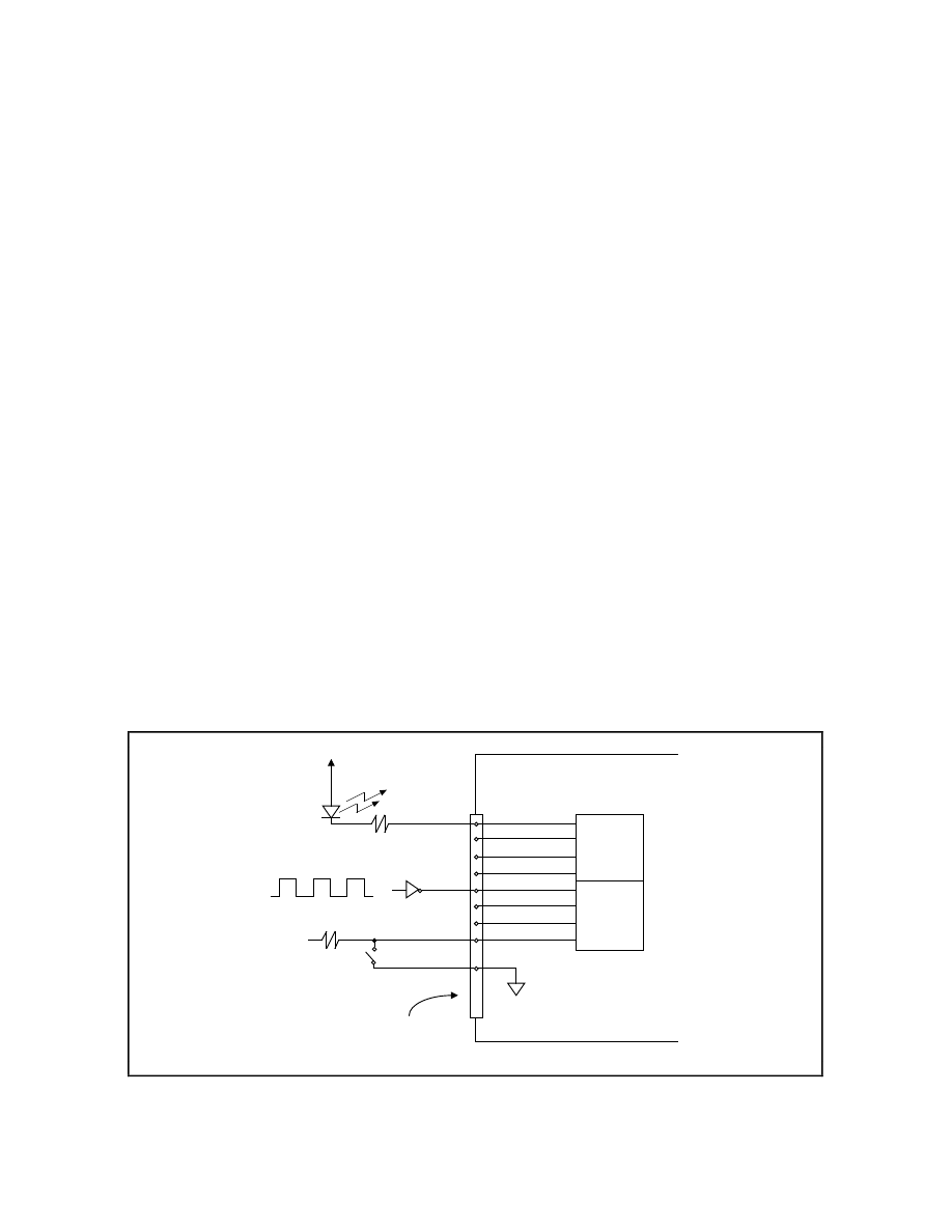
Signal Connections
Chapter 3
AT-MIO-16 User Manual
3-14
© National Instruments Corporation
The following specifications and ratings apply to the digital I/O lines.
•
Absolute maximum voltage input rating
6.0 V with respect to DIGGND
•
Digital input specifications (referenced to DIGGND):
–
V
IH
input logic high voltage
2 V min
–
V
IL
input logic low voltage
0.8 V max
–
I
IH
input current load, logic high input voltage
20
µ
A max
–
I
IL
input current load, logic low input voltage
-20
µ
A max
•
Digital output specifications (referenced to DIGGND):
–
V
OH
output logic high voltage
2.4 V min
–
V
OL
output logic low voltage
0.5 V max
–
I
OH
output source current, logic high
2.6 mA max
–
I
OH
output sink current, logic low
24 mA max
With these specifications, each digital output line can drive 11 standard TTL loads and over
50 LS TTL loads.
Figure 3-8 depicts signal connections for three typical digital I/O applications.
LED
+5 V
TTL Signal
+5 V
Port A
ADIO<3..0>
Port B
BDIO<3..0>
31
29
27
25
32
30
28
26
24
DIGGND
Switch
I/O Connector
AT-MIO-16 Board
Figure 3-8. Digital I/O Connections
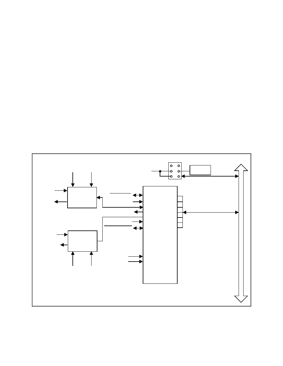
Chapter 3
Signal Connections
© National Instruments Corporation
3-15
AT-MIO-16 User Manual
In Figure 3-8, port A is configured for digital output, and port B is configured for digital input.
Digital input applications include receiving TTL signals and sensing external device states such
as the state of the switch in Figure 3-8. Digital output applications include sending TTL signals
and driving external devices such as the LED shown in Figure 3-8.
Timing I/O Signals
The AT-MIO-16 uses an Am9513A counter/timer for data acquisition timing and for general-
purpose timing I/O functions. An onboard oscillator generates the 10-MHz clock.
RTSI Bus Signal Connections
The AT-MIO-16 is interfaced to the National Instrument RTSI bus. The RTSI bus has seven
trigger lines and a system clock line. You can wire any National Instruments AT Series boards
that have a RTSI bus connector together inside the PC AT and share these signals. Figure 3-9 is
a block diagram of the RTSI bus interface circuitry.
Drivers
R
TSI Bus Connector
W5
RTSICLK
MYCLK
A4
DRV
A4
RCV
STOPTRIG
OUT5
OUT2
GATE1
A2
DRV
A2
RCV
RTSISEL
Internal
Data Bus
B0
B1
B2
B3
B4
B5
B6
A0
A1
A2
A3
A4
A5
A6
RTSI
Switch
/SEL
DATA
OUT1
STARTTRIG
SOURCE5
EXTCONV
FOUT
Trigger
/
7
10 MHz
Oscillator
Drivers
Figure 3-9. RTSI Bus Interface Circuitry Block Diagram

Signal Connections
Chapter 3
AT-MIO-16 User Manual
3-16
© National Instruments Corporation
The RTSI switch is a National Instruments custom integrated circuit that acts as a 7x7 crossbar
switch. Pins B<6..0> are connected to the seven RTSI bus trigger lines. Pins A<6..0> are
connected to seven signals on the board. The RTSI switch can drive any of the signals at pins
A<6..0> onto any one or more of the seven RTSI bus trigger lines and can drive any of the seven
trigger line signals onto any one or more of the pins A<6..0>. This signal trigger produces a
completely flexible signal interconnection scheme for any AT Series board sharing the RTSI bus.
You program the RTSI switch via its select and data inputs.
On the AT-MIO-16 board, nine signals are connected to pins A<6..0> of the RTSI switch with
the aid of additional drivers. The signals GATE1, OUT1, OUT2, OUT5, FOUT, and
STOPTRIG are shared with the AT-MIO-16 I/O connector and Am9513A counter/timer. The
signal SOURCE5 is connected to the Am9513A SOURCE5 pin. The I/O connector and the data
acquisition timing circuitry share the EXTCONV* and STARTTRIG* signals. Through these
onboard interconnections, you can control the AT-MIO-16 general-purpose and data acquisition
timing over the RTSI bus as well as externally, and use the AT-MIO-16 and the I/O connector to
supply timing signals to other AT boards connected to the RTSI bus.
Power Connections
Pins 34 and 35 of the I/O connector supply +5 V from the PC AT power supply. These pins are
referenced to DIGGND and you can use them to power the external digital circuitry.
•
Power rating:
0.5 A at +5 V
±
10%
Warning:
These +5 V power pins should
NOT
be directly connected to analog or digital
ground or to any other voltage source on the AT-MIO-16 or any other device.
Doing so can damage the AT-MIO-16 and the PC AT. National Instruments is
NOT
liable for damages resulting from such a connection.
Timing Connections
Pins 36 through 50 of the I/O connector are connections for timing I/O signals. Pins 36 through
40 carry signals used for data acquisition timing. These signals are explained in the next section,
Data Acquisition Timing Connections. Pins 41 through 50 carry general-purpose timing signals
produced by the onboard Am9513A counter/timer. These signals are explained in the General-
Purpose Timing Signal Connections section later in this chapter.
Data Acquisition Timing Connections
The data acquisition timing signals are SCANCLK, EXTSTROBE*, STARTTRIG*,
STOPTRIG, and EXTCONV*.
SCANCLK is an output signal that generates a high-to-low edge whenever an A/D conversion
begins. SCANCLK pulses only when scanning is enabled on the AT-MIO-16. SCANCLK is
normally high and pulses low for approximately 1
µ
s after the A/D conversion begins. The low-
to-high edge signals that the input signal has been acquired. You can use this signal to clock
external analog input multiplexers. One LS TTL gate drives the SCANCLK signal.
Chapter 3
Signal Connections
© National Instruments Corporation
3-17
AT-MIO-16 User Manual
A low pulse is generated on the EXTSTROBE* pin when the External Strobe Register is
accessed (see the
REG_Level_Write
function in the NI-DAQ Function Reference Manual for
PC Compatibles or the External Strobe Register description in Chapter 2, Register Maps and
Descriptions, of the AT-MIO-16 Register-Level Programmer Manual). Figure 3-10 shows the
timing for the EXTSTROBE* signal.
t
w
100-500 ns
V
OH
t
w
V
OL
Figure 3-10. EXTSTROBE* Signal Timing
The pulse is typically between 100 ns and 500 ns in width. An external device can use the
EXTSTROBE* signal to latch signals or trigger events. The EXTSTROBE* signal is an
LS TTL signal.
The EXTCONV* pin can externally trigger A/D conversions. Applying an active low pulse to
the EXTCONV* signal initiates an A/D conversion. The low-to-high edge of the applied pulse
initiates the A/D conversion. Figure 3-11 shows the timing requirements for the EXTCONV*
signal.
t
w
50 ns minimum
A/D conversion starts within
250 ns from this point
V
IL
V
IH
t
w
tw
Figure 3-11. EXTCONV* Signal Timing
The minimum allowed pulse width is 50 ns. An A/D conversion starts within 250 ns of the low-
to-high edge. There is no maximum pulse-width limitation. EXTCONV* should be high for at
least 50 ns before going low. The EXTCONV* signal is one LS TTL load and is pulled up to
+5 V through a 4.7 k
Ω
resistor.
Note: The output of the Am9513A counter/timer counter 3 also drives EXTCONV*. This
counter is also referred to as the sample-interval counter. You must disable the output
of counter 3 to a high-impedance state if pulses applied to the EXTCONV* pin are to
control A/D conversions. If you use counter 3 to control A/D conversions, you can
monitor its output signal at the EXTCONV* pin.
Signal Connections
Chapter 3
AT-MIO-16 User Manual
3-18
© National Instruments Corporation
An external trigger applied to the STARTTRIG* pin can initiate any data acquisition sequence
that the onboard sample-interval and sample counters control. If the EXTCONV* signal
generates conversions, STARTTRIG* does not affect the acquisition timing. After the two
counters are initialized and armed, applying a falling edge to the STARTTRIG* pin starts the
counters, thereby initiating a data acquisition sequence.
The high-to-low edge of the applied pulse initiates the data acquisition operation. Figure 3-12
shows the timing requirements for the STARTTRIG* signal.
t
w
50 ns minimum
V
IL
V
IH
t
w
tw
First A/D conversion starts within
1 sample interval from this point
Figure 3-12. STARTTRIG* Signal Timing
The minimum allowed pulse width is 50 ns. The first A/D conversion starts within one sample
interval from the high-to-low edge. Counter 3 controls the sample interval.
There is no maximum pulse-width limitation; however, STARTTRIG* should be high for at least
50 ns before going low. The STARTTRIG* signal is one LS TTL load and is pulled up to +5 V
through a 4.7 k
Ω
resistor.
The STOPTRIG pin is used during AT-MIO-16 pretriggered data acquisition operations. In
pretriggered mode, data is acquired but no sample counting occurs until a rising edge is applied
to the STOPTRIG pin. This causes the sample counter to start counting conversions. The
acquisition completes when the sample counter decrements to zero. This mode acquires data
both before and after a hardware trigger is received. Figure 3-13 shows the timing requirements
for the STOPTRIG signal. The STOPTRIG signal is one LS TTL load and is pulled up to +5 V
through a 4.7 k
Ω
resistor.
tw
50 ns minimum
First sample counting occurs within
1 sample interval from this point
t
w
t
w
V
IL
V
IH
STOPTRIG
Figure 3-13. STOPTRIG Signal Timing
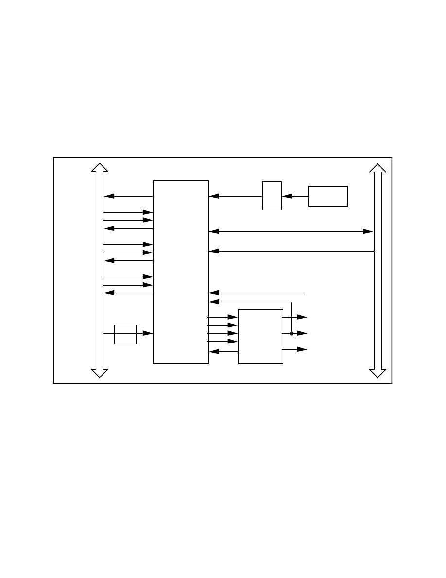
Chapter 3
Signal Connections
© National Instruments Corporation
3-19
AT-MIO-16 User Manual
General-Purpose Timing Signal Connections
The general-purpose timing signals include the GATE, SOURCE, and OUT signals for the
Am9513A counters 1, 2, and 5, and the FOUT signal that the Am9513A generates. You can use
the Am9513A counter/timer counters 1, 2, and 5 for general-purpose applications such as pulse
and square wave generation, event counting, and pulse-width, time-lapse, and frequency
measurements. For these applications, you can directly apply SOURCE and GATE signals to the
counters from the I/O connector and program the counters for various operations. Figure 3-14
shows a block diagram of the timing I/O circuitry.
GATE4
RTSI Bus
/
2
/
16
1 MHz CLK
DATA<15..0>
Am9513 RD/WR
CONVERT
SCANCLK
MUXCTRCLK
Data
Acquisition
Timing
SOURCE4
SOURCE3
OUT1
OUT3
OUT4
OUT5
GATE3
Am9513A
5
Channel
Counter/
Timer
÷
10
GATE5
SOURCE5
OUT5
GATE2
SOURCE2
OUT2
GATE1
SOURCE1
OUT1
FOUT
I/O Connector
STOPTRIG
Flip
Flop
GATE4
PC
A
T
I/O Channel
(10 MHz)
MYCLK
Figure 3-14. Timing I/O Circuitry Block Diagram
The Am9513A contains five independent 16-bit counter/timers, a 4-bit frequency output channel,
and five internally generated timebases. You can program the five counter/timers to operate in
several useful timing modes.
The Am9513A clock input is one-tenth the MYCLK frequency selected by the W5 jumpers. The
factory-default setting for MYCLK is 10 MHz, which generates a 1-MHz clock input to the
Am9513A. The Am9513A uses this clock input to generate five internal timebases. The
counter/timers and the frequency output channel can use these timebases as clocks. When
MYCLK is 10 MHz, the five internal timebases normally used for AT-MIO-16 timing functions
are 1 MHz, 100 kHz, 10 kHz, 1 kHz, and 100 Hz.
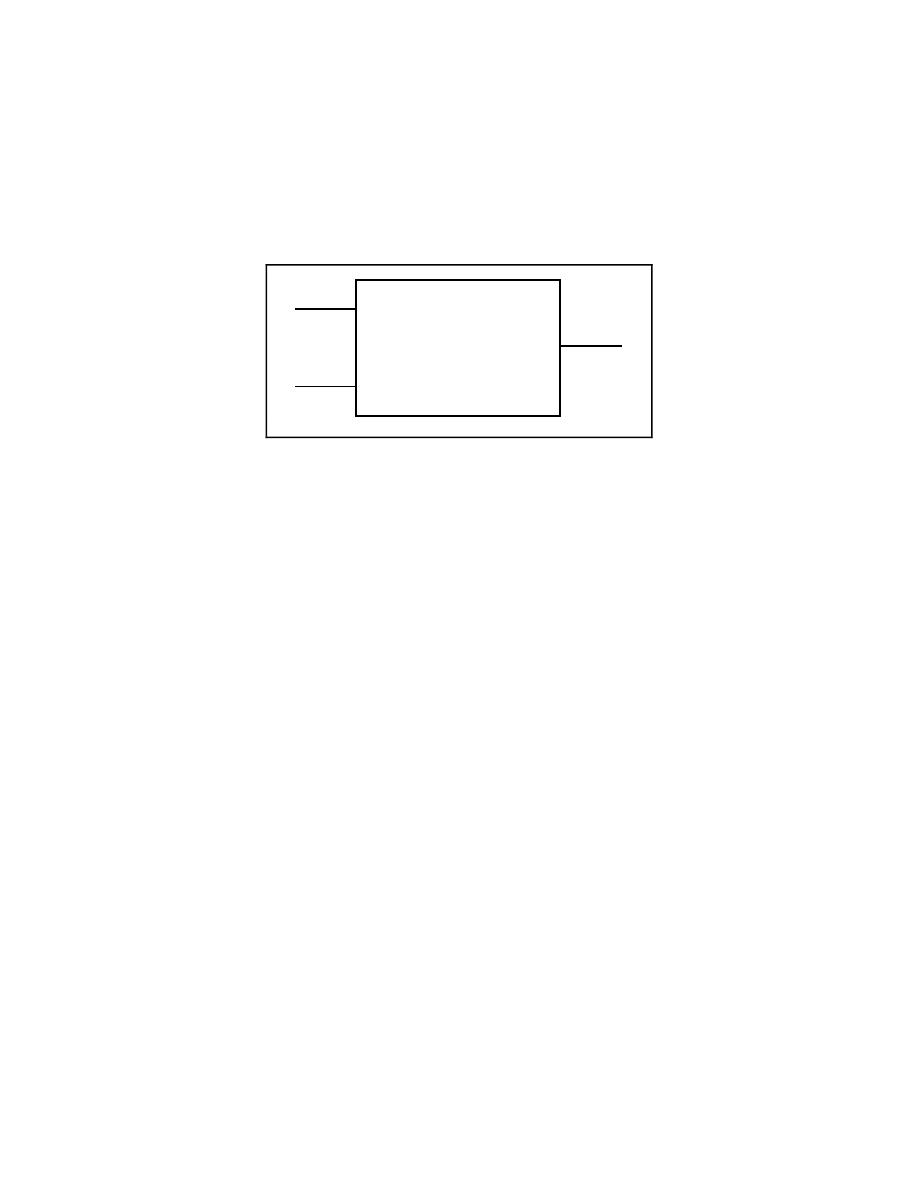
Signal Connections
Chapter 3
AT-MIO-16 User Manual
3-20
© National Instruments Corporation
Note: For detailed programming information, consult the AMD Am9513A Data Sheet
in the AT-MIO-16 Register-Level Programmer Manual. For detailed application
information, consult the Am9513A/Am9513A System Timing Controller technical
manual published by Advanced Micro Devices, Inc.
Figure 3-15 is a diagram of the 16-bit counters in the Am9513A.
SOURCE
GATE
Counter
OUT
Figure 3-15. Counter Block Diagram
Each counter has a SOURCE input pin, a GATE input pin, and an output pin labeled OUT. The
Am9513A counters are numbered 1 through 5, and their GATE, SOURCE, and OUT pins are
labeled GATE N, SOURCE N, and OUT N, where N is the counter number.
For counting operations, you can program the counters to use any of the five internal timebases,
any of the five GATE and five SOURCE inputs to the Am9513A, and the output of the previous
counter (counter 4 uses counter 3 output, and so on). You can configure a counter to count either
falling or rising edges of the selected input.
With the counter GATE input, you can gate counter operation. When you have configured a
counter for an operation through software, a signal at the GATE input can start and stop counter
operation. The Am9513A has five gating modes—no gating, level gating active high, level
gating active low, low-to-high edge gating, and high-to-low edge gating. A counter can also be
active high level gated by a signal at GATE N+1 and GATE N-1, where N is the counter number.
The counter generates timing signals at its OUT output pin. You can also set the OUT output pin
to a high-impedance state or a grounded-output state. The counters generate two types of output
signals during counter operation—terminal-count pulse output and terminal-count toggle output.
Terminal count is often referred to as TC. A counter reaches TC when it counts up or down and
rolls over. In many counter applications, the counter reloads from an internal register when it
reaches TC. In TC pulse output mode, the counter generates a pulse during the cycle that it
reaches TC and reloads. In TC toggle output mode, the counter output changes state after it
reaches TC and reloads. In addition, you can configure the counters for positive logic output or
negative (inverted) logic output for a total of four possible output signals generated for one
timing mode.

Chapter 3
Signal Connections
© National Instruments Corporation
3-21
AT-MIO-16 User Manual
The SOURCE, GATE, and OUT pins for counters 1, 2, and 5 of the onboard Am9513A are
located on the AT-MIO-16 I/O connector. A rising-edge signal on the STOPTRIG pin of the I/O
connector sets the flip-flop output signal connected to the GATE4 input of the Am9513A and
can be used as an additional gate input. The flip-flop output connected to GATE4 is cleared
when the sample counter reaches TC, when an overflow or overrun occurs, or when the A/D
Clear Register is written to.
The Am9513A SOURCE5 pin is connected to the AT-MIO-16 RTSI switch, which means that
you can use a signal from the RTSI trigger bus as a counting source for the Am9513A counters.
You can use the Am9513A OUT2 pin in several different ways. If you configure the board for
the later update mode, an active low pulse on OUT2 updates the analog output on the two DACs.
You can also use OUT2 to trigger interrupt requests. If counter interrupts are enabled, an
interrupt occurs when a rising-edge signal is detected on OUT2. You can use this interrupt to
update the DACs or to interrupt on an external signal connected to OUT2 through the I/O
connector.
Counters 3 and 4 of the Am9513A are dedicated to data acquisition timing and therefore are not
made available for general-purpose timing applications. Signals generated at OUT3 and OUT4
are passed to the data acquisition timing circuitry. The data acquisition timing circuitry controls
GATE3.
Counter 5 is sometimes used by the data acquisition timing circuitry and concatenated with
counter 4 to form a 32-bit sample counter. The SCANCLK signal is connected to the SOURCE3
input of the Am9513A, and OUT1 is sent to the data acquisition timing circuitry. Thus,
counter 1 divides the SCANCLK signal for sequencing the channel-gain memory.
The data acquisition timing circuitry sometimes uses counter 2 to assign a time interval to each
cycle through the scan sequence programmed in the mux-gain memory. This mode is called
interval channel scanning.
The Am9513A 4-bit programmable frequency output channel is provided at the I/O connector
FOUT pin. You can select any of the five internal timebases and any of the counter SOURCE or
GATE inputs as the frequency output source. The frequency output channel divides the selected
source by its 4-bit programmed value and sends the divided down signal at the FOUT pin.
You can produce pulses and square waves at the I/O connector by programming counter 1, 2,
or 5 to generate a pulse signal at its OUT output pin or to toggle the OUT signal each time the
counter reaches the terminal count.
For event counting, program one of the counters to count rising or falling edges applied to any of
the Am9513A SOURCE inputs. You can then read the counter value to determine the number of
edges that have occurred. Counter operation can be gated on and off during event counting.
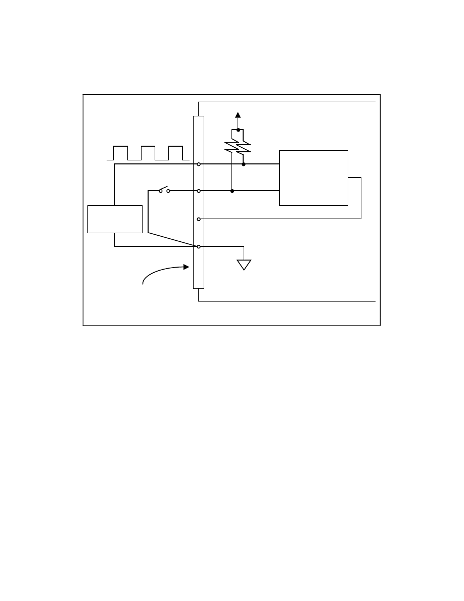
Signal Connections
Chapter 3
AT-MIO-16 User Manual
3-22
© National Instruments Corporation
Figure 3-16 shows connections for a typical event-counting operation in which a switch gates the
counter on and off.
4.7 k
Ω
Signal
Source
Switch
33
DIGGND
Counter
OUT
SOURCE
GATE
+5 V
I/O Connector
AT-MIO-16 Board
Figure 3-16. Event-Counting Application with External Switch Gating
To perform pulse-width measurement, program a counter to be level gated. Apply the pulse to
be measured to the counter GATE input. Program the counter to count while the signal at the
GATE input is either high or low. If the counter is programmed to count an internal timebase,
the pulse width is equal to the counter value multiplied by the timebase period.
For time-lapse measurement, program a counter to be edge gated. Apply an edge to the counter
GATE input to start the counter. You can program the counter to start counting after receiving
either a high-to-low edge or a low-to-high edge. If the counter is programmed to count an
internal timebase, the time lapse since receiving the edge is equal to the counter value multiplied
by the timebase period.
To measure frequency, program a counter to be level gated and to count the rising or falling
edges of a signal applied to a SOURCE input. The gate signal applied to the counter GATE
input is of some known duration. In this case, program the counter to count either rising or
falling edges at the SOURCE input while the gate is applied. The frequency of the input signal is
equal to the count value divided by the known gate period. Figure 3-17 shows the connections
for a frequency measurement application. You could also use a second counter to generate the
gate signal in this application.
Chapter 3
Signal Connections
© National Instruments Corporation
3-23
AT-MIO-16 User Manual
Signal
Source
33
DIGGND
Counter
OUT
SOURCE
GATE
+5 V
4.7 k
Ω
I/O Connector
AT-MIO-16 Board
Gate
Source
Figure 3-17. Frequency Measurement Application
You can concatenate two or more counters by tying the OUT signal from one counter to the
SOURCE signal of another counter. You can then treat the counters as one 32-bit or 48-bit
counter for most counting applications.
The GATE, SOURCE, and OUT signals for counters 1, 2, and 5, and the FOUT output signal are
tied directly from the Am9513A input and output pins to the I/O connector. In addition, the
GATE, SOURCE, and OUT1 pins are pulled up to +5 V through a 4.7 k
Ω
resistor.
The following input and output ratings and timing specifications apply to the Am9513A signals:
•
Absolute maximum voltage input rating
-0.5 V to +7.0 V with respect to DIGGND
•
Am9513A digital input specifications (referenced to DIGGND):
–
V
IH
input logic high voltage
2.2 V min
–
V
IL
input logic low voltage
0.8 V max
–
Input load current
±
10
µ
A max
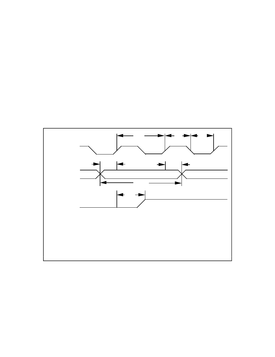
Signal Connections
Chapter 3
AT-MIO-16 User Manual
3-24
© National Instruments Corporation
•
Am9513A digital output specifications (referenced to DIGGND):
–
V
OH
output logic high voltage
2.4 V min
–
V
OL
output logic low voltage
0.4 V max
–
I
OH
output source current, at V
OH
200
µ
A max
–
I
OL
output sink current, at V
OL
3.2 mA max
–
Output current, high-impedance state
±
25
µ
A max
Figure 3-18 shows the timing requirements for the GATE and SOURCE input signals and the
timing specifications for the OUT output signals of the Am9513A.
SOURCE
V
IH
V
IL
V
IH
V
IL
t
sc
t
sp
t
sp
t
gsu
t
gh
t
gw
GATE
t
out
OUT
V
OH
V
OL
sc
t
t
t
t
t
t
145 ns minimum
sp
70 ns minimum
gsu
100 ns minimum
gh
10 ns minimum
gw
145 ns minimum
out
300 ns maximum
Figure 3-18. General-Purpose Timing Signals
The GATE and OUT signal transitions in Figure 3-18 are referenced to the rising edge of the
SOURCE signal. This timing diagram assumes that the counters are programmed to count rising
edges. The same timing diagram, with the source signal inverted and referenced to the falling
edge of the source signal, applies to the case in which the counter is programmed to count falling
edges.

Chapter 3
Signal Connections
© National Instruments Corporation
3-25
AT-MIO-16 User Manual
Any of the Am9513A counter/timers and the Am9513A frequency division output FOUT can use
the signal applied at a SOURCE input as a clock source. The signal applied to a SOURCE input
must not exceed a frequency of 6 MHz for proper operation of the Am9513A. You can
individually program the Am9513A counters to count rising or falling edges of signals applied at
any of the Am9513A SOURCE or GATE input pins.
In addition to the signals applied to the SOURCE and GATE inputs, the Am9513A generates
five internal timebase clocks from the clock signal supplied by the AT-MIO-16. This clock
signal is selected by the W5 jumper and then divided by 10. The factory default value is 1 MHz
into the Am9513A (10 MHz clock signal on the AT-MIO-16). You can use the five internal
timebase clocks as counting sources, and these clocks have a maximum skew of 75 ns between
them. The SOURCE signal shown in Figure 3-18 represents any of the signals applied at the
SOURCE inputs, GATE inputs, or internal timebase clocks.
Specifications for signals at the GATE input are referenced to the signal at the SOURCE input or
one of the Am9513A internally generated signals. Figure 3-18 shows the GATE signal
referenced to the rising edge of a source signal. The gate must be valid (either high or low) at
least 100 ns before the rising or falling edge of a source signal for the gate to take effect at that
source edge as shown by tgsu and tgh in Figure 3-18. Similarly, the gate signal must be held for
at least 10 ns after the rising or falling edge of a source signal for the gate to take effect at that
source edge. The gate high or low period must be at least 145 ns in duration. If you use an
internal timebase clock, the gate signal cannot be synchronized with the clock. In this case, gates
applied close to a source edge take effect either on that source edge or on the next one. This
arrangement creates an uncertainty of one source clock period with respect to unsynchronized
gating sources.
Signals generated at the OUT output are referenced to the signal at the SOURCE input or to one
of the Am9513A internally generated clock signals. Figure 3-18 shows the OUT signal
referenced to the rising edge of a source signal. Any OUT signal state changes occur within
300 ns after the source signal rising or falling edge.
Cabling and Field Wiring
This section describes cabling and field wiring guidelines for the AT-MIO-16 board.
Field Wiring Considerations
Environmental noise can seriously affect the accuracy of measurements made with the
AT-MIO-16 if you do not make proper considerations when running signal wires between signal
sources and the AT-MIO-16 board. The following recommendations mainly apply to analog
input signal routing to the AT-MIO-16 board, although they are applicable for signal routing in
general.

Signal Connections
Chapter 3
AT-MIO-16 User Manual
3-26
© National Instruments Corporation
You can minimize noise pickup and maximize measurement accuracy by doing the following
things:
•
Use individually shielded, twisted-pair wires to connect analog input signals to the
AT-MIO-16. With this type of wire, the signals attached to the CH+ and CH- inputs are
twisted together and then covered with a shield. This shield is then connected at only one
point to the signal source ground. This kind of connection is required for signals traveling
through areas with large magnetic fields or high electromagnetic interference.
•
Use differential analog input connections to reject common-mode noise.
The following recommendations apply for all signal connections to the AT-MIO-16:
•
Physically separate the AT-MIO-16 signal lines from high-current or high-voltage lines.
These lines can induce currents in or voltages on the AT-MIO-16 signal lines if they run in
parallel paths at a close distance. To reduce the magnetic coupling between lines, separate
the lines by a reasonable distance if they run in parallel, or run the lines at right angles to
each other.
•
Do not run the AT-MIO-16 signal lines through conduits that also contain power lines.
•
To protect the AT-MIO-16 signal lines from magnetic fields caused by electric motors,
welding equipment, breakers, or transformers, run the AT-MIO-16 signal lines through
special metal conduits.
Cabling Considerations
National Instruments has a cable termination accessory, the CB-50, for use with the AT-MIO-16
board. This kit includes a terminated, 50-conductor flat ribbon cable and a connector block.
You can attach signal input and output wires to screw terminals on the connector block and
thereby connect to the AT-MIO-16 I/O connector.
The CB-50 is useful for prototyping an application or in situations where AT-MIO-16
interconnections are frequently changed. When you develop a final field wiring scheme,
however, you may want to develop your own cable. This section contains information and
guidelines for designing custom cables.
The AT-MIO-16 I/O connector is a 50-pin male ribbon-cable header. The manufacturer part
numbers for this header that National Instruments uses are as follows:
•
Electronic Products Division/3M (part number 3596-5002)
•
T&B/Ansley Corporation (part number 609-5007)

Chapter 3
Signal Connections
© National Instruments Corporation
3-27
AT-MIO-16 User Manual
The mating connector for the AT-MIO-16 is a 50-position polarized, ribbon-socket connector
with strain relief. National Instruments uses a polarized, keyed connector to prevent inadvertent
upside-down connection to the AT-MIO-16. Recommended manufacturer part numbers for this
mating connector are as follows:
•
Electronic Products Division/3M (part number 3425-7650)
•
T&B/Ansley Corporation (part number 609-5041CE)
The following are standard 50-conductor, 28 AWG, stranded ribbon cables that work with these
connectors:
•
Electronic Products Division/3M (part number 3365/50)
•
T&B/Ansley Corporation (part number 171-50)
In making your own cabling, you may decide to shield your cables. The following guidelines
may help:
•
For the analog input signals, shielded twisted-pair wires for each analog input pair yield the
best results, assuming that you use differential inputs. Tie the shield for each signal pair to
the ground reference at the source.
•
Route the analog lines, pins 1 through 23, separately from the digital lines, pins 24
through 50.
•
When using a cable shield, use separate shields for the analog and digital halves of the cable.
Failure to do so will result in noise from switching digital signals coupling into the analog
signals.

© National Instruments Corporation
4-1
AT-MIO-16 User Manual
Chapter 4
Calibration Procedures
This chapter discusses the calibration procedures for the AT-MIO-16 analog input and analog
output circuitry.
The AT-MIO-16 is calibrated at the factory before shipment. To maintain the 12-bit accuracy of
the AT-MIO-16 analog input and analog output circuitry, check your board’s analog input with a
precise voltage source. If the board is out of calibration, then calibrate it. Otherwise, the board
does not need to be calibrated.
The AT-MIO-16 is factory calibrated in its factory-default configuration:
•
DIFF analog input mode
•
-10 to +10 V analog input range (bipolar)
•
-10 to +10 V analog output range (bipolar with internal reference selected)
Whenever you change your board configuration, recalibrate your AT-MIO-16 board.
Calibration Equipment Requirements
For best measurement results, the AT-MIO-16 needs to be calibrated so that its measurement
accuracy is within
±
0.012% of its input range (
±
1
/
2
LSB). According to standard practice, the
equipment you use to calibrate the AT-MIO-16 should be 10 times as accurate, that is, have
±
0.001% rated accuracy. Practically speaking, calibration equipment with four times the
accuracy of the item under calibration is generally considered acceptable. Four times the
accuracy of the AT-MIO-16 is 0.003%. You need the following equipment to calibrate the
AT-MIO-16 board:
•
For analog input calibration, you need a precision variable DC voltage source (usually a
calibrator) with these features:
–
Accuracy
±
0.001% standard
±
0.003% sufficient
–
Range
Greater than
±
10 V
–
Resolution
100
µ
V in
±
10 V range (5
1
/
2
digits)
•
For analog output calibration, you need a voltmeter with these features:
–
Accuracy
±
0.001% standard
±
0.003% sufficient
–
Range
Greater than
±
10 V
–
Resolution
100
µ
V in
±
10 V range (5
1
/
2
digits)
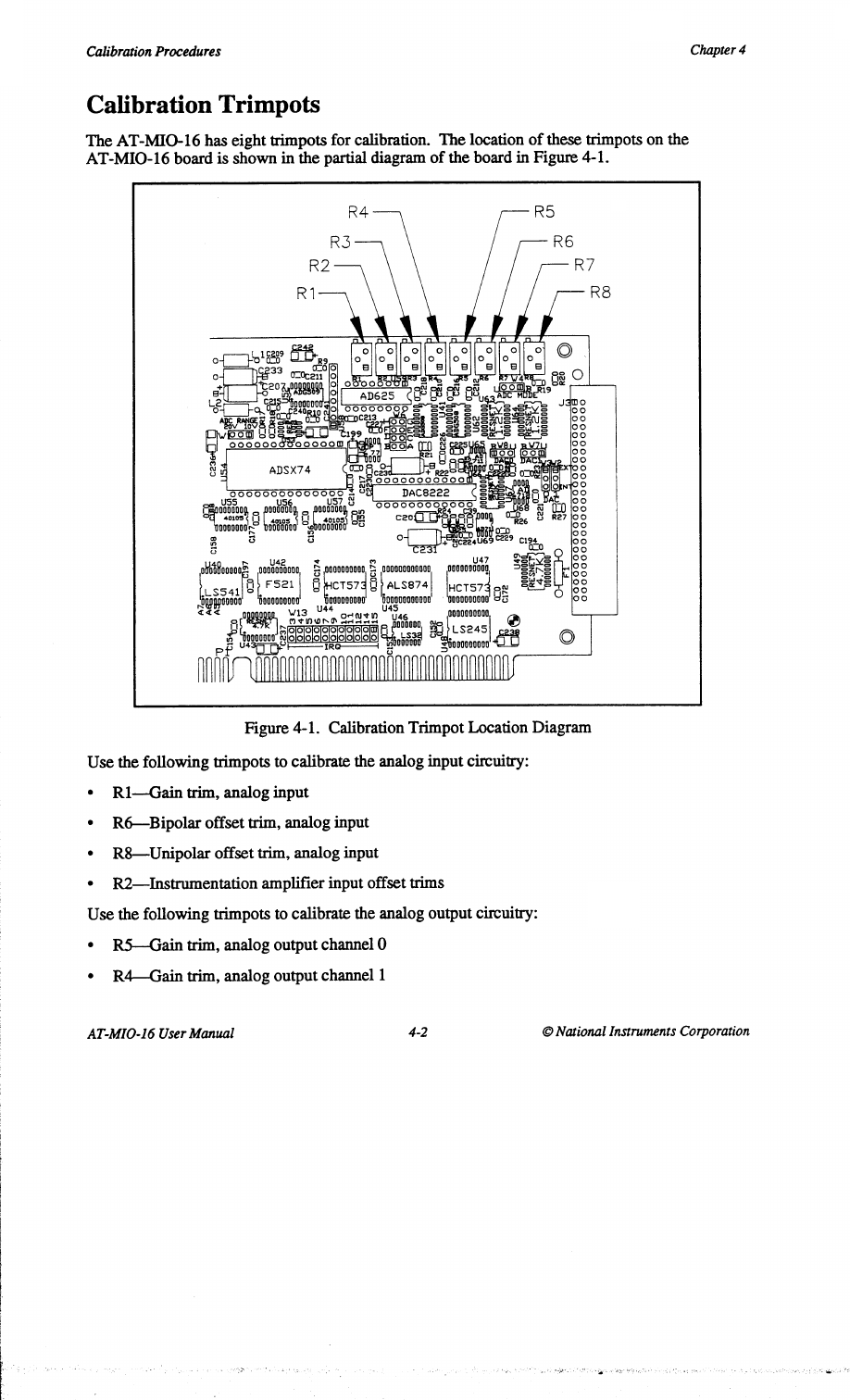

Chapter 4
Calibration Procedures
© National Instruments Corporation
4-3
AT-MIO-16 User Manual
•
R7—Offset trim, analog output channel 0
•
R3—Offset trim, analog output channel 1
Analog Input Calibration
To null error sources that compromise the quality of measurements, you must calibrate the
analog input circuitry by adjusting the following potential sources of error:
•
Offset error at the input of the instrumentation amplifier
•
Offset error at the input of the ADC
•
Gain error of analog input circuitry
Offsets at the input to the instrumentation amplifier contribute gain-dependent offset error to the
analog input circuitry. This offset is multiplied by the gain of the instrumentation amplifier. To
calibrate this offset, you must ground the analog input, read it at two different gain settings, and
adjust a trimpot until the readings match at the two different gain settings.
Offset error at the input of the ADC is the total of the voltage offsets contributed by the circuitry
from the output of the instrumentation amplifier to the ADC input, including the offsets of the
ADC itself. Offset errors appear as a voltage added to the input voltage being measured. To
calibrate this offset, you must apply V
-
fs
+
1
/
2
LSB to the analog input circuitry and adjust a
trimpot until the ADC returns readings that flicker between its most negative count and the most
negative count plus one. The voltages corresponding to V
-
fs
and 1 LSB are given in Table 4-1.
All the stages up to and including the input of the ADC contribute to the gain error of the analog
input circuitry. With the instrumentation amplifier set to a gain of 1, the gain of analog input
circuitry is ideally 1. The gain error is the deviation of the gain from 1 and appears as a
multiplication of the input voltage being measured. To calibrate this offset, you must apply
V
+fs
-
3
/
2
LSB to the analog input circuitry and adjust a potentiometer until the ADC returns
readings that flicker between its most positive count and the most positive count minus 1. The
voltages corresponding to V
+fs
and 1 LSB are given in Table 4-1.
The voltages corresponding to V
-
fs
,
which is the most negative voltage that the ADC can read,
V
+fs
- 1, which is the most positive voltage the ADC can read, and 1 LSB, which is the voltage
corresponding to one count of the ADC, depend on the input range selected. The value of these
voltages for each input range is given in Table 4-1.
Table 4-1. Voltage Values for Calculating Offset Error
Input Range
V
-fs
V
+fs
- 1
1 LSB
1
/
2
LSB
-10 to +10 V
-10 V
+9.99512 V
4.88 mV
2.44 mV
-5 to +5 V
-5 V
+4.99756 V
2.44 mV
1.22 mV
0 to 10 V
0 V
+9.99756 V
2.44 mV
1.22 mV

Calibration Procedures
Chapter 4
AT-MIO-16 User Manual
4-4
© National Instruments Corporation
Board Configuration
The calibration procedure differs depending on the input ranges and input configuration modes
you select. Two analog input calibration procedures are described in the following sections–one
for the two bipolar input configurations (-10 to +10 V and -5 to +5 V), and one for the unipolar
input configuration (0 to +10 V). These calibration procedures assume that your AT-MIO-16 is
configured for DIFF input. If necessary, reconfigure your board for DIFF input before using the
following calibration procedures.
To calibrate your board with a nondifferential input setting, the procedure is similar to the
procedures in this manual with one exception–the following procedures apply the input
calibration voltages across the positive and negative inputs for DIFF channel 0. For single-ended
input, apply your calibration voltages between the channel 0 positive input and the ground
system you are using (refer to Chapter 2, Configuration and Installation, for instructions on
using single-ended input connections).
Bipolar Input Calibration Procedure
If your board is configured for bipolar input, which provides the ranges -5 to +5 V or
-10 to +10 V, then complete the following procedure in the order given. This procedure assumes
that ADC readings are in the range -2,048 to +2,047.
1. Adjust the Amplifier Input Offset
To adjust the amplifier input offset, follow these steps:
a. Connect both ACH0 (pin 3 on the I/O connector) and ACH8 (pin 4) to AISENSE (pin 19).
b. Take analog input readings from channel 0 at the following gains:
•
Both 1 and 500 for the AT-MIO-16L
•
Both 1 and 8 for the AT-MIO-16H
c. Adjust trimpot R2 until the readings match to within one count at both gain settings.
2. Adjust the ADC Input Offset
To adjust the ADC input offset, apply an input voltage across ACH0 and ACH8. This input
voltage is V
-fs
+
1
/
2
LSB and depends on the input range you selected:
Input Range
Calibration Voltage
-10 to +10 V
-9.99756 V
-5 to +5 V
-4.99878 V

Chapter 4
Calibration Procedures
© National Instruments Corporation
4-5
AT-MIO-16 User Manual
a. Connect the calibration voltage across ACH0 (pin 3 on the I/O connector) and ACH8 (pin 4).
Connect the ground point on the calibration voltage source to AISENSE (pin 19).
b. Take analog input readings from channel 0 at a gain of 1 and adjust trimpot R6 until the ADC
readings flicker evenly between -2,048 and -2,047.
3. Adjust the Analog Input Gain
To adjust the analog input gain, apply an input voltage across ACH0 and ACH8. This input
voltage is V
+fs
-
3
/
2
LSB and depends on the input range you selected:
Input Range
Calibration Voltage
-10 to +10 V
-9.99268 V
-5 to +5 V
-4.99634 V
a. Connect the calibration voltage across ACH0 (pin 3 on the I/O connector) and ACH8 (pin 4).
Connect the ground point on the calibration voltage source to AISENSE (pin 19).
b. Take analog input readings from channel 0 at a gain of 1 and adjust trimpot R1 until the ADC
readings flicker evenly between 2,046 and 2,047.
Unipolar Input Calibration Procedure
If your board is configured for unipolar input, which provides an input range of 0 to +10 V, then
complete the following procedure in the order given. This procedure assumes that ADC readings
are in the range 0 to +4,095.
1. Adjust the Amplifier Input Offset
To adjust the amplifier input offset, follow these steps:
a. Connect both ACH0 (pin 3 on the I/O connector) and ACH8 (pin 4) to AISENSE (pin 19).
b. Take analog input readings from channel 0 at a gain of 1 and adjust trimpot R8 until a
reading of roughly two counts is returned.
c. Take analog input readings from channel 0 at the following gains:
•
Both 1 and 500 for the AT-MIO-16L
•
Both 1 and 8 for the AT-MIO-16H
d. Adjust trimpot R2 until the readings at each gain setting match to within one count of each
other.

Calibration Procedures
Chapter 4
AT-MIO-16 User Manual
4-6
© National Instruments Corporation
2. Adjust the ADC Input Offset
To adjust the ADC input offset, apply an input voltage across ACH0 and ACH8. This input
voltage is 1.22 mV, or 0 V +
1
/
2
LSB.
a. Connect the calibration voltage (1.22 mV) across ACH0 (pin 3 on the I/O connector) and
ACH8 (pin 4). Connect the ground point on the calibration voltage source to AISENSE
(pin 19).
b. Take analog input readings from channel 0 at a gain of 1 and adjust trimpot R8 until the ADC
readings flicker evenly between zero and one.
3. Adjust the Analog Input Gain
To adjust the analog input gain, apply an input voltage across ACH0 and ACH8. This input
voltage is +9.99634 V, or V
+fs
-
3
/
2
LSB.
a. Connect the calibration voltage (+9.99634 V) across ACH0 (pin 3 on the I/O connector) and
ACH8 (pin 4). Connect the ground point on the calibration voltage source to AISENSE
(pin 19).
b. Take analog input readings from channel 0 at a gain of 1 and adjust trimpot R1 until the ADC
readings flicker evenly between 4,094 and 4,095.
Analog Output Calibration
To null error sources that affect the accuracy of the output voltages generated, you must calibrate
the analog output circuitry by adjusting the following potential sources of error:
•
Analog output offset error
•
Analog output gain error
Offset error in the analog output circuitry is the total of the voltage offsets that each component
in the circuitry contributes. This error appears as a voltage difference between the desired
voltage and the actual output voltage generated and is independent of the DAC setting. To
correct this offset gain error, set the DAC to negative full scale and adjust a trimpot until the
output voltage is the negative full-scale value
±
1
/
2
LSB.
Gain error in the analog output circuitry is the product of the gains that each component in the
circuitry contributes. This error appears as a voltage difference between the desired voltage and
the actual output voltage generated, which depends on the DAC setting. To correct this gain
error, set the DAC to positive full scale and adjust a trimpot until the output voltage corresponds
to the positive full-scale value
±
1
/
2
LSB.

Chapter 4
Calibration Procedures
© National Instruments Corporation
4-7
AT-MIO-16 User Manual
Board Configuration
The calibration procedure differs depending on whether you select the bipolar or the unipolar
output configuration. A procedure for each configuration is described in the following sections.
These calibration procedures assume that you have selected the internal voltage reference
(+10 V) for the analog output channel to be calibrated.
To calibrate your board to an external reference input (DC only), you must recalculate the
desired output voltages to which you want the board to be calibrated.
•
For bipolar output:
–
1 LSB = V
extref
/2,048 (therefore,
1
/
2
LSB = V
extref
/4,096)
–
V
-fs
= -V
extref
–
V
+fs
= V
extref
- 1 LSB
•
For unipolar output:
–
1 LSB = V
extref
/4,096 (therefore,
1
/
2
LSB = V
extref
/8,192)
–
V
-fs
= 0 V
–
V
+fs
= V
extref
- 1 LSB
To calibrate to your own external reference, you should write your own procedures using the
following procedures as a guide. Substitute your calculated voltages for those given.
Bipolar Output Calibration Procedure
If your board is configured for bipolar output and two's complement mode, which provides an
output range of -10 to +10 V, complete the following procedure in the order given.
1. Adjust the Analog Output Offset
To adjust the analog output offset, measure the output voltage generated with the DAC set at
negative full scale (0). This output voltage should be V
-fs
±
1
/
2
LSB. For bipolar output,
V
-fs
= -10 V, and
1
/
2
LSB = 2.44 mV.
•
For analog output channel 0:
a. Connect the voltmeter between DAC0OUT (pin 20 on the I/O connector) and AOGND
(pin 23).
b. Set the analog output channel to -10 V by writing -2,048 to the DAC.
c. Adjust trimpot R7 until the output voltage read is -10 V
±
2.44 mV, that is, between
-10.00244 V and -9.99756 V.

Calibration Procedures
Chapter 4
AT-MIO-16 User Manual
4-8
© National Instruments Corporation
•
For analog output channel 1:
a. Connect the voltmeter between DAC1OUT (pin 21 on the I/O connector) and AOGND
(pin 23).
b. Set the analog output channel to -10 V by writing -2,048 to the DAC.
c. Adjust trimpot R3 until the output voltage read is -10 V
±
2.44 mV, that is, between
-10.00244 V and -9.99756 V.
2. Adjust the Analog Output Gain
To adjust the analog output gain, measure the output voltage generated with the DAC set at
positive full scale (2,047). This output voltage should be V
+fs
±
1
/
2
LSB. For bipolar output,
V
+fs
= +9.99512 V, and
1
/
2
LSB = 2.44 mV.
•
For analog output channel 0:
a. Connect the voltmeter between DAC0OUT (pin 20 on the I/O connector) and AOGND
(pin 23).
b. Set the analog output channel to +9.99512 V by writing 2,047 to the DAC.
c. Adjust trimpot R5 until the output voltage read is +9.99512 V
±
2.44 mV, that is, between
9.99268 V and 9.99756 V.
•
For analog output channel 1:
a. Connect the voltmeter between DAC1OUT (pin 21 on the I/O connector) and AOGND
(pin 23).
b. Set the analog output channel to +9.99512 V by writing 2,047 to the DAC.
c. Adjust trimpot R4 until the output voltage read is +9.99512 V
±
2.44 mV, that is, between
9.99756 V and 9.99268 V.
Unipolar Output Calibration Procedure
If your analog output channel is configured for unipolar output, which provides an output range
of 0 to +10 V, calibrate your board by performing the following procedure.
1. Adjust the Analog Output Offset
To adjust the analog output offset, measure the output voltage generated with the DAC set at
zero. This output voltage should be V
-fs
±
1
/
2
LSB. For unipolar output, V
-fs
= 0 V, and
1
/
2
LSB = 1.22 mV.

Chapter 4
Calibration Procedures
© National Instruments Corporation
4-9
AT-MIO-16 User Manual
• For analog output channel 0:
a. Connect the voltmeter between DAC0OUT (pin 20 on the I/O connector) and AOGND
(pin 23).
b. Set the analog output channel to 0 V by writing 0 to the DAC.
c. Adjust trimpot R7 until the output voltage read is 0 V
±
1.22 mV.
•
For analog output channel 1:
a. Connect the voltmeter between DAC1OUT (pin 21 on the I/O connector) and AOGND
(pin 23).
b. Set the analog output channel to 0 V by writing 0 to the DAC.
c. Adjust trimpot R3 until the output voltage read is 0 V
±
1.22 mV.
2. Adjust the Analog Output Gain
To adjust the analog output gain, measure the output voltage generated with the DAC set at
positive full scale (4,095). This output voltage should be V
+fs
±
1
/
2
LSB. For unipolar output,
V
+fs
= +9.99756 V, and
1
/
2
LSB = 1.22 mV.
•
For analog output channel 0:
a. Connect the voltmeter between DAC0OUT (pin 20 on the I/O connector) and AOGND
(pin 23).
b. Set the analog output channel to +9.99756 V by writing 4,095 to the DAC.
c. Adjust trimpot R5 until the output voltage read is +9.99756 V
±
1.22 mV, that is, between
9.99634 V and 9.99878 V.
•
For analog output channel 1:
a. Connect the voltmeter between DAC1OUT (pin 21 on the I/O connector) and AOGND
(pin 23).
b. Set the analog output channel to +9.99756 V by writing 4,095 to the DAC.
c. Adjust trimpot R4 until the output voltage read is +9.99756 V
±
1.22 mV, that is, between
9.99634 V and 9.99878 V.
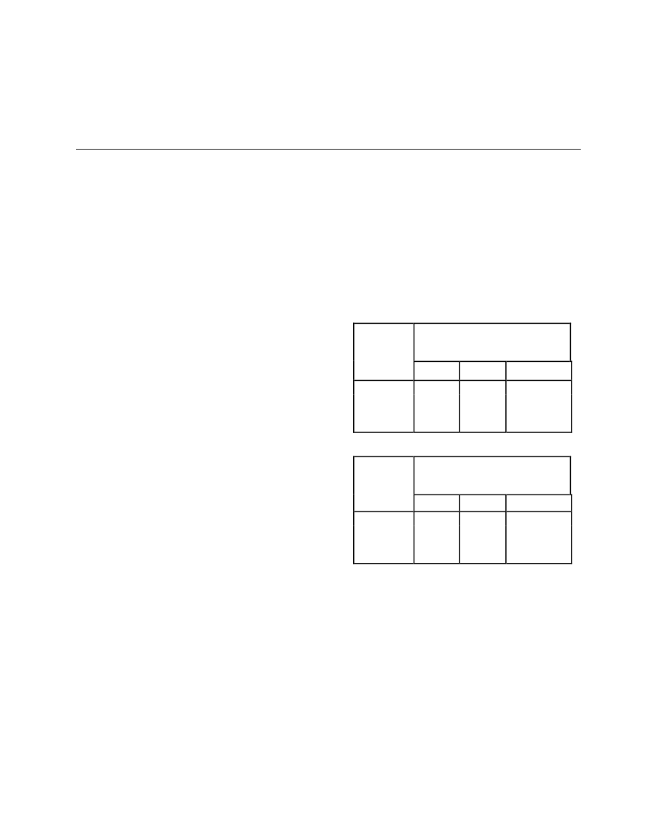
© National Instruments Corporation
A-1
AT-MIO-16 User Manual
Appendix A
Specifications
This appendix lists the specifications for the AT-MIO-16. These specifications are typical at 25
°
C unless otherwise
noted.
Analog Input
Input Characteristics
Number of channels
16 single-ended or 8 differential,
jumper-selectable
Type of ADC
Sampling, successive approximation
Resolution
12 bits, 1 in 4,096
Max sampling rate
100 kS/s
Input signal ranges
AT-MIO-16H and AT-MIO-16DH
Board Gain
(Software
Selectable)
Board Range
(Jumper Selectable)
±
10 V
±
5 V
0 to 10 V
1
±
10 V
±
5
0 to 10 V
2
4
8
±
5 V
±
2.5 V
±
1.25 V
±
2.5
±
1.25 V
±
0.63 V
0 to 5 V
0 to 2.5 V
0 to 1.25 V
AT-MIO-16L and AT-MIO-16DL
Board Gain
(Software
Selectable)
Board Range
(Jumper Selectable)
±
10 V
±
5 V
0 to 10 V
1
±
10 V
±
5
0 to 10 V
10
100
500
±
1 V
±
0.1 V
±
0.02 V
±
0.5
±
0.05 V
±
0.01 V
0 to 1 V
0 to 0.1 V
0 to 0.02 V
Input coupling
DC
Max working voltage (signal + common
mode)
Each input should remain within 12 V
of AIGND
Overvoltage protection
±
35 V powered on,
±
20 V powered off
Inputs protected
ACH <0..15>
FIFO buffer size
16 samples
Data transfers
DMA, interrupts, programmed I/O
DMA modes
Demand
Transfer Characteristics
Relative accuracy
±
0.9 LSB typical,
±
1.5 LSB max
DNL
±
0.50 LSB typical,
±
0.95 LSB max
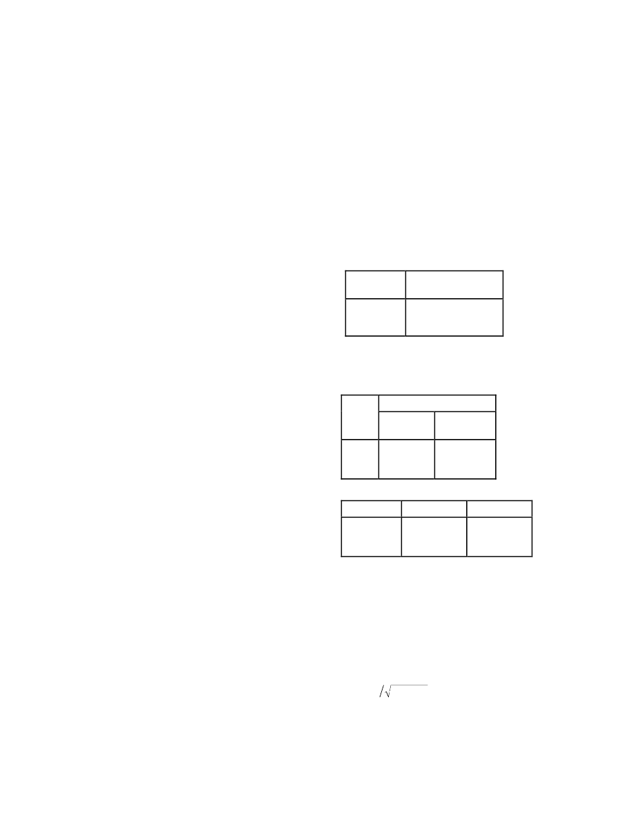
Specifications
Appendix A
AT-MIO-16 User Manual
A-2
© National Instruments Corporation
No missing codes
12 bits, guaranteed
Offset error
Pregain error after calibration
±
2.44
µ
V (-L board)
Pregain error before calibration
±
153
µ
V (-H board)
Postgain error after calibration
±
1.22 mV max
Postgain error before calibration
±
85 V max
Gain error (relative to calibration reference)
After calibration
0.0244% of reading (244 ppm) max
Before calibration
0.85% of reading (8,500 ppm) max
Gain
≠
1 with gain error adjusted to 0
at gain = 1
0.02% of reading (200 ppm) max
Amplifier Characteristics
Input impedance
1 G
Ω
in parallel with 50 pF
Input bias current
±
25 nA
Input offset current
±
15 nA
CMRR
Gain
CMRR
DC to 100 Hz
1
10
100
75 dB
95 dB
105 dB
Dynamic Characteristics
Bandwidth
Small signal (-3 dB)
650 kHz @ gain = 1
Settling time to full-scale step
Gain
Accuracy
±
0.024%
(
±
1 LSB)
±
0.012%
(
±
0.5 LSB)
≤
10
100
500
10
µ
s
14
µ
s
47
µ
s
10
µ
s
14
µ
s
50
µ
s
System noise (including quantization error)
Gain
20 V Range
10 V Range
≤
10
100
500
0.10 LSBrms
0.15 LSBrms
0.30 LSBrms
0.20 LSBrms
0.20 LSBrms
0.40 LSBrms
Slew rate
5.0 V/
µ
s
Stability
Recommended warm-up time
15 min
Offset temperature coefficient
Pregain
6
µ
V/
°
C
Postgain
160
µ
V/
°
C
Onboard calibration reference
Level
2.5 V
±
10 mV
Temperature coefficient
10 ppm/
°
C max
Long-term stability
20 ppm
1, 000 hr

Appendix A
Specifications
© National Instruments Corporation
A-3
AT-MIO-16 User Manual
Analog Output
Output Characteristics
Number of channels
2 voltage
Resolution
12 bits, 1 in 4,096
Max update rate
250 kS/s
Type of DAC
Double-buffered, multiplying
Data transfers
Interrupts, programmed I/O
Transfer Characteristics
Relative accuracy (INL)
Bipolar range
±
0.25 LSB typical,
±
0.5 LSB max
Unipolar range
±
0.50 LSB typical,
±
1.0 LSB max
DNL
±
0.2 LSB typical,
±
1 LSB max
Monotonicity
12 bits, guaranteed
Offset error
After calibration
488
µ
V max
Before calibration
±
64 mV max
Gain error (relative to internal reference)
After calibration
±
0.017% of reading (170 ppm) max
Before calibration
±
0.77% of reading (7,700 ppm) max
Voltage Output
Ranges
±
10 V, 0–10 V, jumper selectable
Output coupling
DC
Output impedance
≤
0.2
Ω
Current drive
±
2 mA max
Protection
Short-circuit protection
Power-on state
Undetermined
External reference input
Range
±
10 V
Overvoltage protection
±
25 V powered on
Input impedance
11 k
Ω
Dynamic Characteristics
Settling time to 0.024% FSR
4
µ
s for a 20 V step
Slew rate
30 V/
µ
s
Noise
1 mVrms, DC to 1 MHz

Specifications
Appendix A
AT-MIO-16 User Manual
A-4
© National Instruments Corporation
Digital I/O
Number of channels
8 I/O
Compatibility
TTL
Digital logic levels
Level
Min
Max
Input low voltage
Input high voltage
Input low current
(Vin = 0.4 V)
Input high current
(Vin = 2.7 V)
0 V
2 V
0.8 V
6 V
-20
µ
A
20
µ
A
Output low voltage
(Iout = 24 A)
Output high voltage
(Iout = -2.6 A)
2.4 V
0.5 V
Power on state
Configured as input
Data transfers
Programmed I/O
Timing I/O
Number of channels
3 counter/timers, 1 frequency scalers
Resolution
Counter/timers
16 bits
Frequency scalers
4 bits
Compatibility
TTL, pulled high with 4.7 k
Ω
resistors
Base clocks available
1 MHz, 100 kHz, 10 kHz, 1 kHz, 100 Hz
Base clock accuracy
±
0.01 %
Max source frequency
6.897 MHz
Min source pulse duration
70 ns
Min gate pulse duration
145 s
Data transfers
Programmed I/O
Triggers
Digital Trigger
Compatibility
TTL
Response
Falling edge
Pulse width
50 ns min
RTSI
Trigger lines
7
Bus Interface
Slave

Appendix A
Specifications
© National Instruments Corporation
A-5
AT-MIO-16 User Manual
Power Requirement
+5 VDC (
±
5 %)
1.6 A
Physical
Dimensions
13.3 by 3.9 in. (33.782 by 9.906 cm)
I/O connector
50-pin male ribbon connector
Form factor
AT
Environment
Operating temperature
0
°
to 70
°
C
Storage temperature
-55
°
to 150
°
C
Relative humidity
5% to 90% noncondensing

© National Instruments Corporation
B-1
AT-MIO-16 User Manual
Appendix B
Revisions A through C
Parts Locator Diagram
This appendix contains the parts locator diagram for revisions A through C of the AT-MIO-16
board.
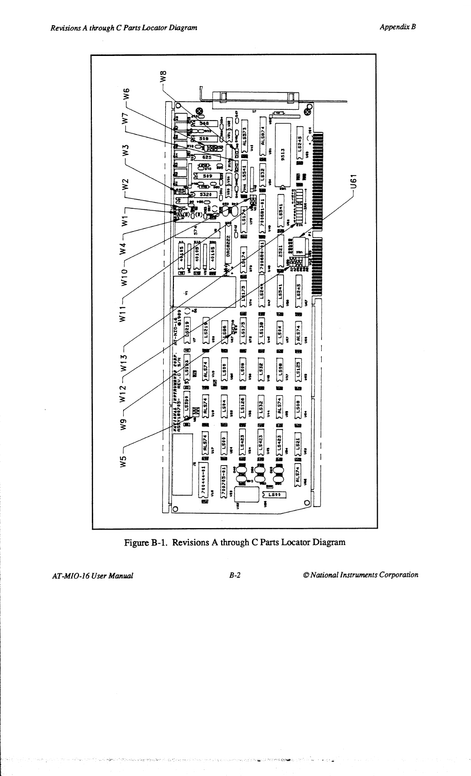

© National Instruments Corporation
C-1
AT-MIO-16 User Manual
Appendix C
Customer Communication
For your convenience, this appendix contains forms to help you gather the information necessary
to help us solve technical problems you might have as well as a form you can use to comment on
the product documentation. Filling out a copy of the Technical Support Form before contacting
National Instruments helps us help you better and faster.
National Instruments provides comprehensive technical assistance around the world. In the U.S.
and Canada, applications engineers are available Monday through Friday from 8:00 a.m. to
6:00 p.m. (central time). In other countries, contact the nearest branch office. You may fax
questions to us at any time.
Corporate Headquarters
(512) 795-8248
Technical support fax: (800) 328-2203
(512) 794-5678
Branch Offices
Phone Number
Fax Number
Australia
(03) 879 9422
(03) 879 9179
Austria
(0662) 435986
(0662) 437010-19
Belgium 02/757.00.20
02/757.03.11
Denmark
45 76 26 00
45 76 71 11
Finland
(90) 527 2321
(90) 502 2930
France
(1) 48 14 24 00
(1) 48 14 24 14
Germany
089/741 31 30
089/714 60 35
Italy 02/48301892
02/48301915
Japan
(03) 3788-1921
(03) 3788-1923
Mexico
95 800 010 0793
95 800 010 0793
Netherlands 03480-33466
03480-30673
Norway 32-848400
32-848600
Singapore
2265886
2265887
Spain
(91) 640 0085
(91) 640 0533
Sweden
08-730 49 70
08-730 43 70
Switzerland
056/20 51 51
056/20 51 55
Taiwan
02 377 1200
02 737 4644
U.K.
0635 523545
0635 523154

Technical Support Form
___________________________________________________
Photocopy this form and update it each time you make changes to your software or hardware, and use the completed
copy of this form as a reference for your current configuration. Completing this form accurately before contacting
National Instruments for technical support helps our applications engineers answer your questions more efficiently.
If you are using any National Instruments hardware or software products related to this problem, include the
configuration forms from their user manuals. Include additional pages if necessary.
Name
Company
Address
Fax (
)
Phone (
)
Computer brand
Model
Processor
Operating system
Speed
MHz
RAM
MB
Display
adapter
Mouse
yes
no
Other adapters installed
Hard disk capacity
MB
Brand
Instruments used
National Instruments hardware product model
Revision
Configuration
National Instruments software product
Version
Configuration
The problem is
List any error messages
The following steps will reproduce the problem

AT-MIO-16 Hardware and Software
Configuration Form
Record the settings and revisions of your hardware and software on the line to the right of each item. Complete a
new copy of this form each time you revise your software or hardware configuration, and use this form as a
reference for your current configuration. Completing this form accurately before contacting National Instruments
for technical support helps our applications engineers answer your questions more efficiently.
National Instruments Products
•
AT-MIO-16 Model Number (For example,
AT-MIO-16L-9)
_____________________________________________
•
AT-MIO-16 Revision
_____________________________________________
•
Interrupt Level of AT-MIO-16
(Factory Setting: 10)
_____________________________________________
•
DMA Channels of AT-MIO-16
(Factory Setting: 6 and 7)
_____________________________________________
•
Base I/O Address of AT-MIO-16
(Factory Setting: hex 0220)
_____________________________________________
•
Programming Choice
(NI-DAQ, LabVIEW, LabWindows or other)
_____________________________________________
•
Software Version
_____________________________________________
Other Products
•
Computer Make and Model
_____________________________________________
•
Microprocessor
_____________________________________________
•
Clock Frequency
_____________________________________________
•
Type of Video Board Installed
_____________________________________________
•
Operating System (DOS or Windows)
_____________________________________________
•
Operating System Version
_____________________________________________
•
Programming Language
_____________________________________________
•
Programming Language Version
_____________________________________________
•
Other Boards in System
_____________________________________________
•
Base I/O Address of Other Boards
_____________________________________________
•
DMA Channels of Other Boards
_____________________________________________
•
Interrupt Level of Other Boards
_____________________________________________

Documentation Comment Form
National Instruments encourages you to comment on the documentation supplied with our products. This
information helps us provide quality products to meet your needs.
Title:
AT-MIO-16 User Manual
Edition Date:
February 1995
Part Number:
320476-01
Please comment on the completeness, clarity, and organization of the manual.
If you find errors in the manual, please record the page numbers and describe the errors.
Thank you for your help.
Name
Title
Company
Address
Phone (
)
Mail to:
Technical Publications Department
Fax to:
Technical Publications Department
National Instruments Corporation
National Instruments Corporation
6504 Bridge Point Parkway, MS 53-02
MS 53-02
Austin, TX 78730-5039
(512) 794-5678
Register-Level Programmer Manual
Request Form
National Instruments offers a register-level programmer manual at no charge to customers who are not using
National Instruments software.
Title:
AT-MIO-16 Register-Level Programmer Manual
Part Number:
340695-01
Please indicate your reasons for obtaining the register-level programmer manual. Check all that apply.
National Instruments does not support your operating system or programming language.
You are an experienced register-level programmer who is more comfortable writing your own register-level
software.
Other. Please explain.
Thank you for your help.
Name
Title
Company
Address
Phone (
)
Mail to:
Data Entry Department
Fax to:
Data Entry Department
National Instruments Corporation
National Instruments Corporation
6504 Bridge Point Parkway
(512) 794-8411
Austin, TX 78730-5039
© National Instruments Corporation
Glossary-1
AT-MIO-16 User Manual
Glossary
___________________________________________________
Prefix
Meaning
Value
p-
pico-
10-
12
n-
nano-
10-
9
µ
-
micro-
10-
6
m-
milli-
10-
3
k-
kilo-
10
3
M-
mega-
10
6
G-
giga-
10
9
%
percent
±
plus or minus
˚
degrees
/
per
+
positive of, or plus
–
negative of, or minus
≠
not equal to
√
square root of
+5V
+5 VDC source signal
A
amperes
AC
alternating current
ACH
analog input channel signal
A/D
analog-to-digital
ADC
A/D converter
ADIO
digital input/output port A signal
AIGND
analog input ground signal
AISENSE
analog input sense signal
ANSI
American National Standards Institute
AOGND
analog output ground signal
AWG
American Wire Gauge
BDIO
digital input/output port B signal
C
Celsius
CMRR
common-mode rejection ratio
CVI
C Virtual Instrument
D/A
digital-to-analog
DAC
D/A converter
DAC0WR
analog channel 0 output
DAC1WR
analog channel 1 output
dB
decibels
DC
direct current
DIFF
differential mode

Glossary
LabWindows User Manual
Glossary-2
© National Instruments Corporation
DIGGND
digital ground signal
DIP
dual inline package
DMA
direct memory access
EISA
Extended Industry Standard Architecture
EXTCONV
external Convert Signal
EXTREF
external reference signal
EXTSTROBE
external strobe signal
FIFO
first-in-first-out
FSR
full-scale ratio
ft
feet
hex
hexadecimal
Hz
hertz
in.
inches
INL
integral nonlinearity
I/O
input/output
IRQ
interrupt lines
I
IH
current, input high
I
IL
current, input low
I
OH
current, output high
I
OL
current, output low
LED
light-emitting diode
LS
low-power Schottky
LSB
least significant bit
max
maximum
min
minimum
MSB
most significant bit
mux
multiplexer
NRSE
nonreferenced single-ended mode
Ω
ohms
OUT
output
PC
personal computer
ppm
parts per million
rms
root mean square
RSE
referenced single-ended mode
RTSI
Real-Time System Integration
RTSICLK
Real-Time System Integration clock
s
seconds
S
samples
SCANCLK
scan clock signal
SCXI
Signal Conditioning eXtensions for Instrumentation
SDK
Software Developer’s Toolkit
SE
single-ended inputs
S/H
sample and hold
STARTTRIG
external trigger signal
STOPTRIG
stop trigger signal
TC
terminal count
THD
total harmonic distortion
TTL
transistor-transistor logic
V
volts

Glossary
© National Instruments Corporation
Glossary-3
LabWindows User Manual
VDC
volts direct current
V
fs
output offset voltage
V
IH
volts, input high
V
IL
volts, input low
V
in
volts in
V
OH
volts, output high
V
OL
volts, output low
V
ref
reference voltage
Vrms
volts, root mean square

© National Instruments Corporation
Index-1
AT-MIO-16 User Manual
Index
Numbers/Symbols
+5 V pin
definition, 3-3
warning against connecting to
ground, 3-16
A
ACH<O..15> signal
description, 3-2
input ranges and maximum ratings, 3-5
ADIO<0..3> signal, 3-3, 3-13
AIGND signal, 3-2, 3-4
AISENSE signal, 3-3
analog input calibration, 4-3 to 4-6
bipolar input calibration procedure, 4-4
to 4-5
board configuration, 4-4
unipolar input calibration procedure, 4-5
to 4-6
analog input configuration, 2-8 to 2-12
DIFF (differential) input, 2-9
factory settings, 2-6 to 2-7
input mode, 2-9
input polarity and range, 2-10 to 2-11
jumper settings quick reference (table),
2-6 to 2-7
NRSE input (16 channels), 2-10
RSE input (16 channels), 2-9 to 2-10
selecting input ranges, 2-11 to 2-12
actual range and precision vs. range
selection and gain (table), 2-12
analog input signal connections
instrumentation amplifier, 3-5 to 3-6
pin descriptions, 3-3 to 3-4
warning against exceeding input
ranges, 3-5
analog input specifications, A-1 to A-2
amplifier characteristics, A-2
dynamic characteristics, A-2
input characteristics, A-1
stability, A-2
transfer characteristics, A-1
analog output calibration, 4-6 to 4-9
bipolar output calibration procedure, 4-7
to 4-8
board configuration, 4-7
unipolar output calibration procedure,
4-8 to 4-9
analog output configuration, 2-12 to 2-15
circuitry block diagram, 2-13
data coding, 2-14
data mode (table), 2-15
output range selection and precision
(table), 2-15
jumper settings quick reference (table),
2-6 to 2-7
output reference, 2-13 to 2-14
internal and external reference
selection (table), 2-14
polarity selection, 2-14
bipolar and unipolar (table), 2-15
output range selection and precision
(table), 2-15
RTSI bus clock selection, 2-17
analog output signal connections, 3-12
to 3-13
analog output specifications, A-3
dynamic characteristics, A-3
output characteristics, A-3
transfer characteristics, A-3
voltage output, A-3
AOGND signal, 3-3, 3-13
AT bus interface configuration, 2-1 to 2-5
base I/O address selection, 2-3 to 2-4
DMA channel selection, 2-4 to 2-5
factory default settings (table), 2-1
interrupt selection, 2-5
parts locator diagram
revision D and later, 2-2
revisions A through C, B-2
AT-MIO-16. See also specifications.
definition of, ix
description of, 1-1
interface with SCXI systems, 1-1
parts locator diagram
revision D and later, 2-2
revisions A through C, B-2

Index
AT-MIO-16 User Manual
Index-2
© National Instruments Corporation
software programming choices, 1-2
to 1-5
LabVIEW and LabWindows
software, 1-2 to 1-3
NI-DAQ driver software, 1-3 to 1-4
register-level programming, 1-5
unpacking, 1-5
what you need to get started, 1-1
AT-MIO-16 instrumentation amplifier, 3-5
to 3-6
B
base I/O address configuration, 2-3 to 2-4
example switch settings
(illustration), 2-3
factory default settings (table), 2-1
switch settings with corresponding base
I/O address and base I/O address
space (table), 2-4
verifying the address space, 2-3
BDIO<0..3> signal, 3-3, 3-13
bipolar input
calibration procedure, 4-4 to 4-5
configuration, 2-10 to 2-11
bipolar output
calibration procedure, 4-7 to 4-8
configuration, 2-14 to 2-15
board configuration. See calibration
procedures; configuration.
bus interface specifications, A-4
C
cabling considerations, 3-26 to 3-27
calibration procedures
analog input calibration, 4-3 to 4-6
bipolar input calibration procedure,
4-4 to 4-5
board configuration, 4-4
unipolar input calibration procedure,
4-5 to 4-6
analog output calibration, 4-6 to 4-9
bipolar output calibration procedure,
4-7 to 4-8
board configuration, 4-7
unipolar output calibration
procedure, 4-8 to 4-9
equipment requirements, 4-1
trimpots, 4-2
common mode signal rejection
considerations, 3-11 to 3-12
configuration. See also installation; jumper
settings; signal connections.
analog input configuration, 2-8 to 2-12
data acquisition circuitry block
diagram, 2-8
DIFF (differential) input, 2-9
input mode, 2-9
input polarity and range, 2-10 to 2-11
NRSE input (16 channels), 2-10
RSE input (16 channels), 2-9 to 2-10
selecting input ranges, 2-11 to 2-12
actual range and precision vs.
range selection and gain
(table), 2-12
analog I/O jumper settings quick
reference (table), 2-6 to 2-7
analog output configuration, 2-12
to 2-15
block diagram, 2-13
data coding, 2-14
data mode (table), 2-15
output range selection and
precision (table), 2-15
output reference, 2-13 to 2-14
external reference selection
(table), 2-14
internal reference selection
(table), 2-14
polarity selection, 2-14
bipolar and unipolar (table), 2-15
output range selection and
precision (table), 2-15
AT bus interface, 2-1 to 2-5
base I/O address selection, 2-3 to 2-4
DMA channel selection, 2-4 to 2-5
factory default settings (table), 2-1
interrupt selection, 2-5
base I/O address selection, 2-3 to 2-4
AT bus factory default settings
(table), 2-1
example switch settings
(illustration), 2-3

Index
© National Instruments Corporation
Index-3
AT-MIO-16 User Manual
switch settings with corresponding
base I/O address and base I/O
address space (table), 2-4
verifying the address space, 2-3
cabling considerations, 3-26 to 3-27
digital I/O configuration, 2-15 to 2-16
DMA channel selection, 2-4 to 2-5
AT bus factory default settings
(table), 2-1
jumper settings (table), 2-5
field wiring considerations, 3-25 to 3-26
interrupt selection, 2-5
AT bus factory default settings
(table), 2-1
jumper settings (table), 2-5
overview, 2-1
parts locator diagram, B-2
revision D and later, 2-2
revisions A through C, B-2
RTSI bus clock selection, 2-17
customer communication, x, C-1
D
DAC0OUT signal, 3-3, 3-12
DAC1OUT signal, 3-3, 3-12
data acquisition timing connections, 3-16
to 3-25
EXTCONV* signal, 3-17
EXTSTROBE* signal, 3-16 to 3-17
SCANCLK signal, 3-16
STARTTRIG* signal, 3-18
STOPTRIG signal, 3-18
data mode configuration
analog output data coding, 2-14
straight binary (table), 2-15
two's complement (table), 2-15
differential connections
floating signal sources, 3-8 to 3-9
general considerations, 3-7
ground-referenced signal sources, 3-8
differential input
configuration, 2-9
definition, 2-9
DIGGND signal, 3-3, 3-13
digital I/O
configuration, 2-15 to 2-16
signal connections, 3-13 to 3-15
specifications, A-4
DMA channel
configuration, 2-4 to 2-5
factory default settings (table), 2-1
jumper settings (table), 2-5
documentation
conventions used in the manual, x
organization, ix
related documentation, x
E
environment noise, minimizing, 3-25 to 3-26
environment specifications, A-5
event counting, 3-21
event-counting application with external
switch gating (illustration), 3-22
EXTCONV* signal
description, 3-4
RTSI switch connections, 3-16
timing connections, 3-17
external reference selection (table), 2-14
EXTREF signal, 3-3, 3-12
EXTSTROBE* signal, 3-3, 3-17
F
fax technical support, C-1
field wiring considerations, 3-25 to 3-26
floating signal sources
description, 3-6
differential connections, 3-8 to 3-9
recommended configurations (table), 3-7
single-ended connections, 3-10
FOUT signal, 3-4, 3-16, 3-25
frequency measurement, 3-22 to 3-23
fuse, 3-3
G
GATE, OUT, and SOURCE timing signals,
3-19 to 3-25
GATE1 signal, 3-4, 3-16
GATE2 signal, 3-4
GATE3 signal, 3-21
GATE5 signal, 3-4

Index
AT-MIO-16 User Manual
Index-4
© National Instruments Corporation
general-purpose connections, 3-19 to 3-25
counter block diagram, 3-20
event-counting application with external
switch gating (illustration), 3-22
frequency measurement, 3-22 to 3-23
frequency measurement application
(illustration), 3-23
GATE, SOURCE, and OUT signals,
3-19 to 3-25
input and output ratings, 3-23 to 3-24
time-lapse measurement, 3-22
timing I/O circuitry block diagram, 3-19
timing requirements (illustration), 3-24
timing signals, 3-19 to 3-25
ground-referenced signal sources
definition and requirements, 3-6
differential connections, 3-8
recommended configurations (table), 3-7
single-ended connections, 3-11
H
hardware installation, 2-17 to 2-18
I
input configurations
common mode signal rejection, 3-11
to 3-12
differential input
floating signal sources, 3-8 to 3-9
general considerations, 3-7
ground-referenced signal
sources, 3-8
recommended configurations for ground-
referenced and floating signal
sources (table), 3-7
single-ended connections
floating signal (RSE) sources, 3-10
general considerations, 3-10
grounded signal (NRSE)
sources, 3-11
input polarity, configuring. See polarity
configuration.
installation. See also configuration.
hardware installation, 2-17 to 2-18
unpacking the AT-MIO-16, 1-5
instrumentation amplifier, 3-5 to 3-6
internal reference selection (table), 2-14
interrupts
configuration, 2-5
factory default settings (table), 2-1
jumper settings (table), 2-5
I/O connector pin assignments, 3-1 to 3-2
signal description, 3-3 to 3-4
J
jumper settings
analog input
DIFF (differential) input
configuration, 2-9
input polarity and range (table), 2-11
NRSE input (16 channels), 2-10
RSE input (16 channels), 2-9 to 2-10
analog I/O jumper settings quick
reference (table), 2-6 to 2-7
analog output
data mode settings (table), 2-15
polarity settings (table), 2-15
AT bus interface settings, 2-1
factory default settings (table), 2-1
base I/O address, 2-3
example settings (illustration), 2-3
switch settings with base I/O address
and address space (table), 2-4
bipolar output selection (table), 2-15
DMA selection, 2-4 to 2-5
external reference selection (table), 2-14
input polarity and input range
(table), 2-11
internal reference factory setting
(table), 2-14
interrupt selection, 2-5
overview, 2-1
RTSI bus clock selection, 2-17
straight binary mode (table), 2-15
two's complement mode (table), 2-15
unipolar output selection (table), 2-15
L
LabVIEW software, 1-2 to 1-3
LabWindows software, 1-2 to 1-3

Index
© National Instruments Corporation
Index-5
AT-MIO-16 User Manual
N
NI-DAQ driver software, 1-3 to 1-4
interface with programming
languages, 1-4
relationship between programming
environment, NI-DAQ, and
hardware (illustration), 1-4
noise, minimizing, 3-25 to 3-26
nonreferenced single-ended (NRSE) input
configuration, 2-10
definition, 2-10
single-ended connections for grounded
signal sources, 3-11
NRSE input. See nonreferenced single-
ended (NRSE) input.
O
OUT, GATE, and SOURCE timing signals,
3-19 to 3-25
OUT1 signal, 3-4, 3-16
OUT2 signal, 3-4, 3-16, 3-21
OUT3 signal, 3-21
OUT4 signal, 3-21
OUT5 signal, 3-4, 3-16
output polarity, configuring. See polarity
configuration.
P
physical specifications, A-5
pin assignments for I/O connector, 3-2
polarity calibration procedure
bipolar input, 4-4 to 4-5
bipolar output, 4-7 to 4-8
unipolar input, 4-5 to 4-6
unipolar output, 4-8 to 4-9
polarity configuration
input polarity and input range, 2-10
to 2-11
actual range and precision vs. range
selection and gain (table), 2-12
considerations for selecting, 2-11
to 2-12
jumper settings (table), 2-11
output polarity, 2-14
jumper settings (table), 2-15
output range and precision
(table), 2-15
power connections, 3-16
power requirement specifications, A-5
programming, register-level, 1-5. See also
software for AT-MIO-16 board.
pulse-width measurement, 3-22
pulses, producing, 3-21
R
referenced single-ended (RSE) input
configuration, 2-9 to 2-10
definition, 2-9
single-ended connections for floating
signal sources, 3-10
register-level programming, 1-5
RSE input. See referenced single-ended
(RSE) input.
RTSI bus
clock selection, 2-17
definition, 1-1
signal connections, 3-15 to 3-16
block diagram, 3-15
RTSI switch, 3-16
S
SCANCLK signal
data acquisition timing connections, 3-16
description, 3-3
general-purpose timing, 3-21
SCXI systems, 1-1
signal connections
analog input signal connections, 3-4
to 3-6
instrumentation amplifier, 3-5 to 3-6
warning against exceeding input
ranges, 3-5
analog output signal connections, 3-12
to 3-13
cabling considerations, 3-26 to 3-27
digital I/O signal connections, 3-13
to 3-15
field wiring considerations, 3-25 to 3-26
floating signal sources, 3-6

Index
AT-MIO-16 User Manual
Index-6
© National Instruments Corporation
ground-referenced signal sources, 3-6
input configurations
common mode signal rejection, 3-11
to 3-12
differential connections
floating signal sources, 3-8 to 3-9
general considerations, 3-6
grounded signal sources, 3-8
recommended configurations for
ground-referenced and floating
signal sources (table), 3-7
single-ended connections
floating signal (RSE) sources, 3-10
general considerations, 3-10
grounded signal (NRSE)
sources, 3-11
pin assignments for I/O connector, 3-2
pin descriptions, 3-3 to 3-4
power connections, 3-16
RTSI bus signal connections, 3-15
to 3-16
timing connections, 3-16 to 3-18
data acquisition timing connections,
3-16 to 3-18
general-purpose connections, 3-19
to 3-25
pins for, 3-16
timing I/O signals, 3-15
types of signal sources, 3-5
warning against exceeding ratings, 3-1
single-ended connections
floating signal (RSE) sources, 3-10
general considerations, 3-10
grounded signal (NRSE) sources, 3-11
single-ended input configuration
NRSE input (16 channels), 2-10
RSE input (16 channels), 2-9 to 2-10
software for AT-MIO-16 board
LabVIEW and LabWindows, 1-2 to 1-3
NI-DAQ driver software, 1-3 to 1-4
register-level programming, 1-5
SOURCE, OUT, and GATE timing signals,
3-19 to 3-25
SOURCE1 signal, 3-4
SOURCE2 signal, 3-4
SOURCE3 signal, 3-21
SOURCE5 signal, 3-4, 3-16, 3-21
specifications
analog input, A-1 to A-2
analog output, A-3
bus interface, A-4
digital I/O, A-4
environment, A-5
physical, A-5
power requirement, A-5
RTSI trigger lines, A-4
timing I/O, A-4
triggers, A-4
square waves, producing, 3-21
STARTTRIG* signal
description, 3-3
RTSI switch connections, 3-16
timing connections, 3-18
STOPTRIG* signal
data acquisition timing connections, 3-18
description, 3-3
RTSI switch connections, 3-16
straight binary mode output selection
(table), 2-15
switch settings. See jumper settings.
T
technical support, C-1
time-lapse measurements, 3-22
timing connections, 3-16 to 3-18
data acquisition timing connections, 3-16
to 3-18
EXTCONV signal, 3-17
EXTSTROBE signal, 3-17
SCANCLK signal, 3-16
STARTTRIG* signal, 3-18
STOPTRIG* signal, 3-18
general-purpose connections, 3-19
to 3-25
counter block diagram, 3-20
event-counting application with
external switch gating
(illustration), 3-22
frequency measurement, 3-22
frequency measurement application
(table), 3-23
GATE, SOURCE, and OUT signals,
3-19 to 3-25
input and output ratings, 3-23 to 3-24
time-lapse measurement, 3-22

Index
© National Instruments Corporation
Index-7
AT-MIO-16 User Manual
timing I/O circuitry block
diagram, 3-19
timing requirements
(illustration), 3-24
timing signals, 3-19 to 3-25
pins for, 3-16
timing I/O signals, 3-15
timing I/O specifications, A-4
trigger specifications, A-4
two's complement mode (table), 2-15
U
unipolar input
calibration procedure, 4-5 to 4-6
configuration, 2-10 to 2-11
unipolar output
calibration procedure, 4-8 to 4-9
configuration, 2-14 to 2-15
unpacking the AT-MIO-16, 1-5
Document Outline
- AT-MIO-16 User Manual
- Contents
- About This Manual
- Chapter 1 Introduction
- Chapter 2 Configuration and Installation
- Chapter 3 Signal Connections
- I/O Connector
- Signal Descriptions
- Analog Input Signal Connections
- Types of Signal Sources
- Input Configurations
- Differential Connection Considerations (DIFF Configuration)
- Differential Connections for Grounded Signal Sources
- Differential Connections for Floating Signal Sources
- Single-Ended Connection Considerations
- Single-Ended Connections for Floating Signal Sources (RSE Configuration)
- Single-Ended Connections for Grounded Signal Sources (NRSE Configuration)
- Common-Mode Signal Rejection Considerations
- Analog Output Signal Connections
- Digital I/O Signal Connections
- Timing I/O Signals
- RTSI Bus Signal Connections
- Power Connections
- Timing Connections
- Signal Descriptions
- Cabling and Field Wiring
- I/O Connector
- Chapter 4 Calibration Procedures
- Calibration Equipment Requirements
- Calibration Trimpots
- Analog Input Calibration
- Analog Output Calibration
- Appendix A Specifications
- Appendix B Revisions A through C Parts Locator Diagram
- Appendix C Customer Communication
- Glossary
- Index
- Figures
- Figure 1-1. The Relationship between the Programming Environment, NI-DAQ, and Your Hardware
- Figure 2-1. AT-MIO-16 Parts Locator Diagram
- Figure 2-2. Example Base I/O Address Switch Settings
- Figure 2-3. Analog Input and Data Acquisition Circuitry Block Diagram
- Figure 2-4. Analog Output Circuitry Block Diagram
- Figure 2-5. Digital I/O Circuitry Block Diagram
- Figure 3-1. AT-MIO-16 I/O Connector Pin Assignments
- Figure 3-2. AT-MIO-16 Instrumentation Amplifier
- Figure 3-3. Differential Input Connections for Grounded Signal Sources
- Figure 3-4. Differential Input Connections for Floating Signal Sources
- Figure 3-5. Single-Ended Input Connections for Floating Signal Sources
- Figure 3-6. Single-Ended Input Connections for Grounded Signal Sources
- Figure 3-7. Analog Output Connections
- Figure 3-8. Digital I/O Connections
- Figure 3-9. RTSI Bus Interface Circuitry Block Diagram
- Figure 3-10. EXTSTROBE* Signal Timing
- Figure 3-11. EXTCONV* Signal Timing
- Figure 3-12. STARTTRIG* Signal Timing
- Figure 3-13. STOPTRIG Signal Timing
- Figure 3-14. Timing I/O Circuitry Block Diagram
- Figure 3-15. Counter Block Diagram
- Figure 3-16. Event-Counting Application with External Switch Gating
- Figure 3-17. Frequency Measurement Application
- Figure 3-18. General-Purpose Timing Signals
- FigureÊ4-1. Calibration Trimpot Location Diagram
- Figure B-1. Revisions A through C Parts Locator Diagram
- Tables
- Table 2-1. AT Bus Interface Factory-Default Settings
- Table 2-2. Switch Settings with Corresponding Base I/O Address and Base I/O Address Space
- Table 2-3. DMA Jumper Settings
- Table 2-4. Interrupt Jumper Settings
- Table 2-5. Analog I/O Jumper Settings Quick Reference
- Table 2-6. DIFF Input Configuration (Factory Setting)
- Table 2-7. RSE Input Configuration
- Table 2-8. NRSE Input Configuration
- Table 2-9. Configurations for Input Range and Input Polarity
- Table 2-10. Actual Range and Measurement Precision Versus Input Range Selection and Gain
- Table 2-11. Internal and External Reference Selection
- Table 2-12. Analog Output Polarity and Data Mode Configuration
- Table 2-13. Output Range Selection and Precision
- Table 2-14. Configurations for RTSI Bus Clock Selection
- Table 3-1. Recommended Input Configurations for Ground-Referenced and Floating Signal Sources
- Table 4-1. Voltage Values for Calculating Offset Error
Wyszukiwarka
Podobne podstrony:
09&16 S User Manual Eng
Monitor 16 9 22 cale Acer AL2202W User Manual
cas test platform user manual
CARPROG Opel ECU programmer user manual
elm327 interface viecar obd2 bluetooth scanner user manual
autel power scan ps100 user manual
Chartplanner user manual
INPA User manual
all100 user manual
CARPROG user manual
FX2N 485 BD User's Manual JY992 Nieznany
mb sbc tool user manual
07 Altistart48 user manual
iphone user manual pdf
PRDM 0010 Upgrade user manual UPG 0001
TK105 GPS Tracker User Manual
ATDSK1118 User Manual
FX2N 232 IF User's Manual JY992D66701
Protek 3502C USER MANUAL
więcej podobnych podstron