456719261


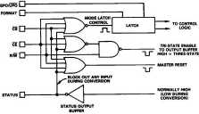
Figurę 7. Control Logic Błock Diagram
OPERATION
WRITE/CONVERT
READ
NONĘ
NONĘ
CONTROL AND TIMING OF THE AD670 Control Logic
The AD670 contains on-chip logie to provide conyęrsion and data read operations from signals commonly available in micro-processor systems. Figurę 7 shows the internal logie circuitry of the AD670. The control signals, CE, CS, and R/W control the operation of the converter. The read or write function is deter-mined by R/W when both CS and CE are Iow as shown in Table II. If all three control inputs are held Iow longer than the conversion time, the device will continuously convert until one input, CE, CS, or R/W is brought high. The relative timing of these signals is discussed later in this section.
Table II. AD670 Control Signal Truth Table
Timing
The AD670 is easily interfaced to a variety of microprocessors and other digital systems. The following discussion of the timing reąuirements of the AD670 control signals will provide the designer with useful insight into the operation of the device. Write/Convert Start Cycle
Figurę 8 shows a complete timing diagram for the write/convert start cycle. CS (chip select) and CE (chip enable) are active Iow and are interchangeable signals. Both CS and CE must be Iow for the converter to read or start a conyęrsion. The minimum pulse width, %, on either CS or CE is 300 ns to start a conyęrsion.
REV. A
Table III. AD670 TIMING SPECIFICATIONS
|
Symbol |
Parameter |
@ +2S°C Min Typ Max |
Units |
|
WRITE/CONYERT START MODĘ | |||
|
tw |
Write/Start Pulse Width |
300 |
ns |
|
Input Data Setup Time |
200 |
ns | |
|
tfJH |
Input Data Hołd |
10 |
ns |
|
tmvY' |
Read/Write Setup Before Control |
0 |
ns |
|
tnc |
Delay to Convert Start |
700 |
ns |
|
tc |
Conyęrsion Time |
10 |
ps |
|
READ MODĘ | |||
|
tR |
Read Time |
250 |
ns |
|
Delay from Status Low to Data Read |
250 |
ns | |
|
Bus Access Time |
200 250 |
ns | |
|
tpH |
Data Hołd Time |
25 |
ns |
|
tDT |
Output Float Delay |
150 |
ns |
|
tRT |
R/W before CE or CS low |
0 |
ns |
-7-
Wyszukiwarka
Podobne podstrony:
6 (388) ?=• FIGURĘ 13-16 Błock diagrams of (<?) a dojne and {b) a hasin. Notę that m a domc the o
P1020415 Figurę 3.1. The błock diagram of a simple Computer with hardwired control. 0000 0001 INA
2` CIRCUIT OPERATION Figurę 5 shows a błock diagram of the FM wireless microphone Circuit The microp
metro {H Untitled l.vi Błock Diagram File Edit View Project Operate Tools Window Help 0 # © II &
zad3a ® Zad3.viZad3.vi Błock Diagram File Edit View Project Operate lools Window Help m File Edit
zad3b ® Zad3.vi Błock Diagram File Edit View Project Operate lools Window Help® II fidUggo* m Start
5 (434) (a) Figurę 13-15 Piuugmc fol*. (:ł) A schcmanc lilustration of a plunging fold. (4) A błock
P1020412 3. The błock diagram of a simple example Computer with microprogrammed contro! (presented o
ms0 błąd bmp lab_ME_LV_1 .vi Błock Diagram File Edit View Project Operate lools Window Help ConteKt
Pentium(r) III Processor Architectural Błock Diagram System Bus 1 Fetch/Decode Control Micro Codę
J> zadanie2.vi Błock Diagram - ffjx. File Edit View Project Operate Tools Window
więcej podobnych podstron