Modeling and Design of a Micromechanical Phase-Shifting Gate Optical Modulator
Long Que, G. Witjaksono and Y.B. Gianchandani
Department of Electrical and Computer Engineering
University of Wisconsin – Madison, WI, USA, que@cae.wisc.edu
ABSTRACT
This paper reports the modeling and design of a
micromechanical optical modulator with a phase-shifting
gate that utilizes optical interference effects to modulate
light. The gate is opened or closed by microactuators
integrated on the same chip, modulating light beams
between stationary optical fibers. Modeling results show
optimized designs can have high modulation efficiency of
99.5%, and contrast ratio of 23 dB. Alignment between
fibers is guaranteed by guiding grooves available in
standard MEMS batch fabrication techniques, which also
permits coupling distance between fibers to be minimized.
The insertion loss for a typical design can be less than –1.9
dB. The beam profile shows negligible distortion for 40
µ
m
or lower coupling distances.
Keywords: Phase-shifting gate, MEMS, optical interference
effects, optical modulation, reflectivity.
1 INTRODUCTION
Low-cost and highly reliable optical devices are needed
to implement optical communication networks. Several
optical switches have been developed to modulate the
optical path using standard microelectromechanical system
techniques in the past [1-5]. The most common approach
has been to use micromirrors, which present the challenge
of high reflectivity and smoothness. The best reflectivity
reported to date has been 85% (-0.71dB) by which is
achieved by coating gold on a silicon mirror. The
roughness of mirror is about 5 nm with proper fabrication
process [1].
In this report, a new design of a micromechanical
modulator is demonstrated using a phase-shifting gate,
which can be driven by microactuators integrated on the
same chip. The gate alters the phase of propagated light in
the optical system and consequently modulates light by
optical interference effects. Modeling efforts show that
minimum reflectivity of zero and maximum reflectivity of
99.5
%
by can be achieved by optimizing the optical
systems. The wavelength
λ
0
= 1.55
µ
m is used in our
calculations because it is widely used for fiber-optic
communication and it is highly transparent and lossless for
silicon [6]. Using a phase-shifting gate instead of
micromirror simplifies the gate fabrication process [7]: for
example, there is no need for a gold evaporation to improve
the reflectivity of the gate surface. The coupling distance
between fibers can readily be reduced to less than 40
µ
m.
Fiber alignment is guaranteed by guiding grooves available
in standard micromachining process. The scattering of
incident light by the gate is negligible since the roughness of
the sidewall of the phase-shifting gate can be reduced to
several nanometers [1,2,7], while the wavelength for optical
communication is generally 1.3
µ
m or 1.55
µ
m, which is
about 2 orders of magnitude larger than the surface
roughness.
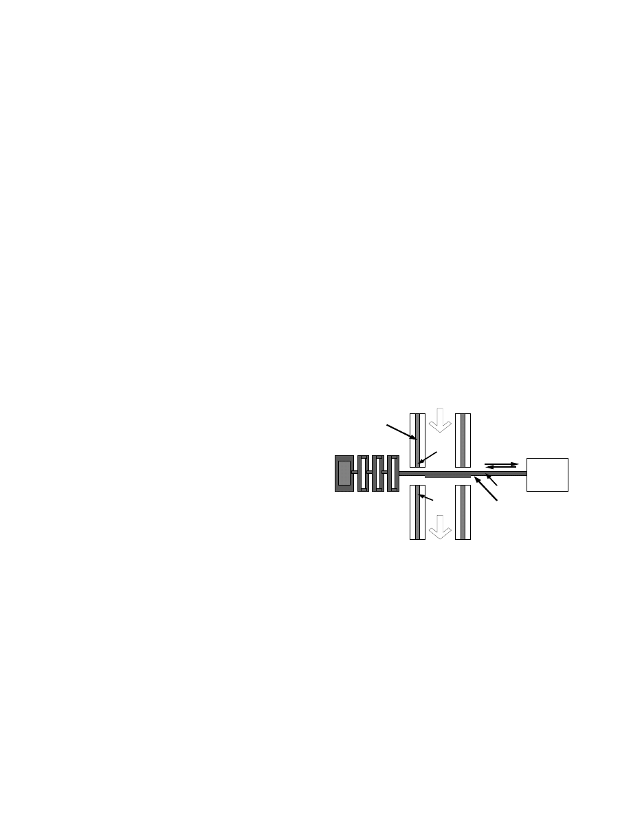
Fiber 1
Fiber 3
Input
Fiber 2
Fiber 4
Output
Actuator
Spring
Fiber Core
Phase-shifting gate
with different
thickness
n2
n4
n1
n5
n3
Gate movement
direction
Figure 1: Schematic top view of a typical micromechanical
optical modulator
2 DEVICE STRUCTURE
A typical device structure is shown in Figure 1. It
consists of a phase-shifting gate with varying thickness.
The gate is laterally actuated by integrated electrostatic or
an electro-thermal actuators [8,9]. When the gate moves
from the right to the left or vice versa, the optical path
thickness between fiber 1 and fiber 2 or fiber 3 and fiber 4
will vary, modulating the light due to constructive or
destructive optical interference effects.
n1
n2
n3
n4
n5
Light
T2 T3
T4
fiber core
air
gap Gate
air
gap fiber core
T1
T5
Figure 2: Modeling of the layered structure of the
optical modulator system
3 MODELING
The micromechanical optical modulator can be treated
as a layered structure optical system for modeling purposes
(Figure 2). Here, T
2
and T
4
are the thicknesses of the air
gaps, T
3
is the thickness of the phase-shifting gate and
n
1
(n
5
), n
2
(n
4
), n
3
are the optical refraction indexes of fiber
core, air and the gate. Assume the light from fiber is
incident at an angle of
θ
1
to the air gap layer (Figure 2), so
the characteristic matrix of the optical system is given by
[10]:
cos
β
2
-i/n
2
sin
β
2
cos
β
3
-i/n
3
sin
β
3
M =
×
×
-in
2
sin
β
2
cos
β
2
-in
3
sin
β
3
cos
β
3
cos
β
4
-i/n
4
sin
β
4
(1)
-in
4
sin
β
4
cos
β
4
and the relative reflectivity of the optical system is given
by:
2
1
22
21
1
5
12
11
1
22
21
1
5
12
11
)
(
)
(
)
(
)
(
P
M
M
P
P
M
M
P
M
M
P
P
M
M
R
+
+
+
+
−
+
=
(2)
where
β
i
=2
π
/
λ
0
n
i
T
i
cos
θ
i
(i=2,3,4) and P
i
=n
i
cos
θ
i
(i=1,5),
θ
i
is the refraction angle in the media with refraction index of
n
i
(i=1,2,3,4,5).
4 OPTIMIZATION
4.1 Structure Dimension Optimization
In the following study assume light wavelength
λ
0
=
1.55
µ
m and
θ
1
= 0 radian. The design of the system would
be successful if parameters T
2
*
, T
3
*
and T
4
*
could be found
for relative reflectivity equal zero or close to unity with a
prescribed accuracy:
0
)
,
,
,
(
1
*
4
*
3
*
2
=
θ
T
T
T
R
(3)
or
1
)
,
,
,
(
1
*
4
*
3
*
2
≈
θ
T
T
T
R
(4)
This is a multi-objective optimization problem. A Matlab
TM
program has been developed to solve this problem using
ATTGOAL routine for the optimization [11]. Like most
optimization procedures, this algorithm relies on the starting
values of optimization parameters, T
2
0
, T
3
0
and T
4
0
. A proper
choice of their values can reduce the computation time. For
example, take the starting values to be: T
2
0
= T
4
0
= 20
µ
m,
and T
3
0
= 5
µ
m, and the required accuracy as 10
-4
. For zero
reflectivity, the optimized design parameters will be
T
2
*
=T
4
*
=20.09
µ
m, and T
3
*
=5.30
µ
m, while for maximum
reflectivity, the optimized design parameters will be
T
2
*
=T
4
*
=19.76
µ
m, and T
3
*
=4.98
µ
m.
The algorithm outlined above has applicability for
generalized multilayer optics. For the specific example of
Figure 2, it provides the intuitively obvious result that the
reflectivity is maximum when T
2
and T
4
are odd multiples of
λ
0
/4n
2
, and T
3
is an odd multiple of
λ
0
/4n
3
. Additionally, the
reflectivity is zero when T
3
is even multiple of
λ
0
/4n
3
. The
analytical formula for these specific conditions can be
obtained from equation (1) and (2) as following:
2
3
3
2
2
2
2
3
2
1
3
1
3
3
2
2
2
2
3
2
1
sin
)
(
cos
2
sin
)
(
β
β
β
n
n
n
n
n
i
n
n
n
n
n
n
i
R
+
+
−
−
=
(5)
The reflectivity versus the gate thickness relationship based
on equation (5) is shown in Figure 3. It shows clearly that
the light beam can be modulated by the thickness of the gate
for the specific dimensional designs.
0
2
4
6
8
1 0
0
0 .2
0 .4
0 .6
0 .8
1
G a te T h ic k n e s s (T 3 )
Rel
a
ti
ve Re
fl
ecti
v
it
y
n 3 = 4 .0 n 3 = 3 .5
n 3 = 3 .0
Figure 3: The modulating properties of the layered structure
optical system, T
3
in units of
λ
0
/4n
3
. The modulation
efficiency increases with n
3
, n
1
=1.467, n
2
=1.
θ
1
Fiber 1
Fiber 3
Input
Fiber 2
Fiber 4
Output
Actuator
Spring
Fiber Core
Silicon Plate
Figure 4: Schematic top view of an optimized design of
optical modulator with buffer silicon plates
0
2
4
6
8
1 0
0
0 .2
0 .4
0 .6
0 .8
1
G a t e T h i c k n e s s
R
e
la
ti
ve
r
e
fl
ec
ti
v
ity
Figure 5: Modulating properties of the layered structure
optical system with silicon gates. T
gate
in units of
λ
0
/4n
gate
.
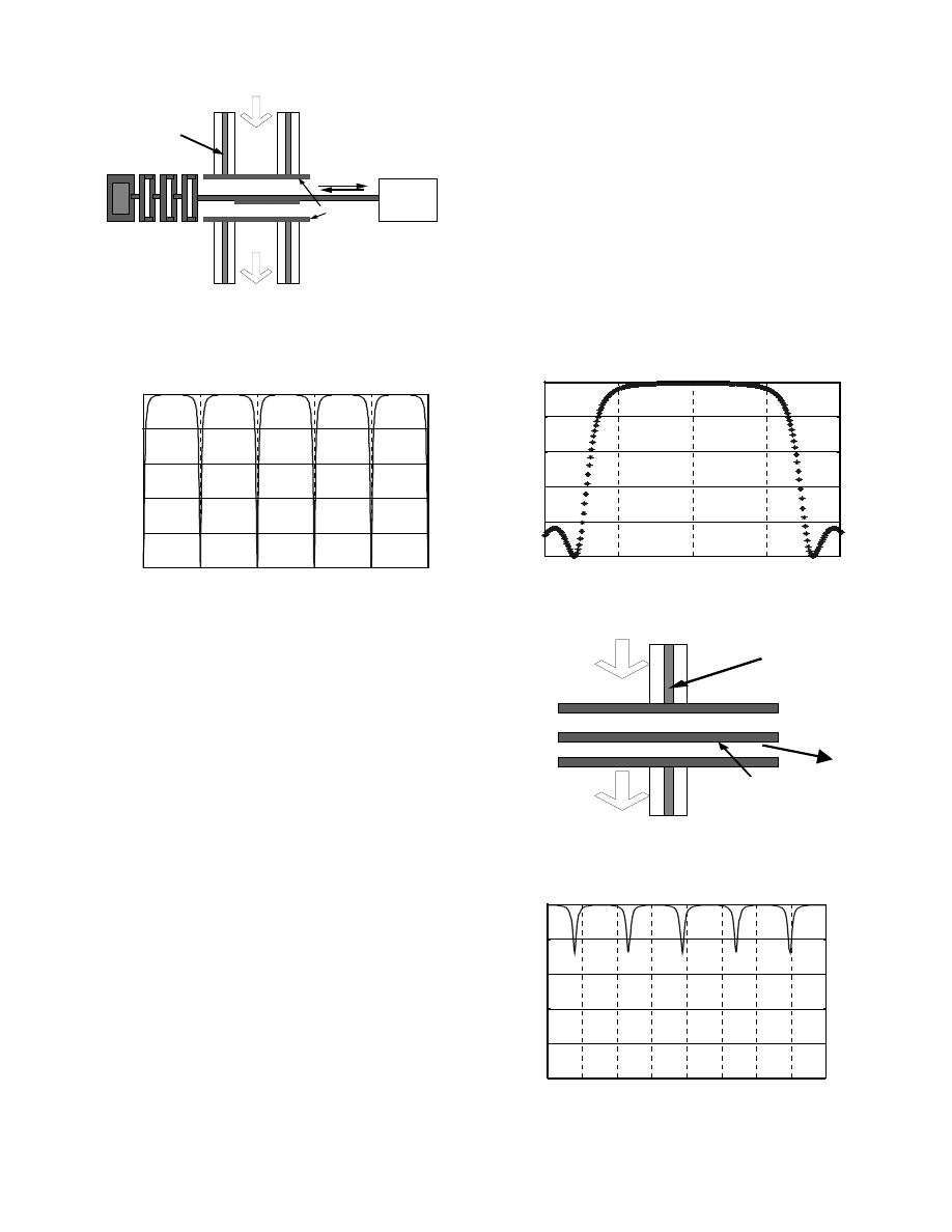
4.2 System Architecture Optimization
The modulation efficiency can be improved by
modifying the system design. Figure 4 shows the buffer
silicon plates that are integrated to the optical system to
improve the modulation efficiency as well as to assist
assembly of the optical fibers. Figure 5 gives the
modulation properties of this system with a silicon gate,
showing 99.5% modulation and 23 dB contrast ratio can be
achieved when the thickness of silicon plates is designed to
be odd multiple of
λ
0
/4n
silicon
and the air gaps are also odd
multiple of
λ
0
/4n
air
.
5 DESIGN CONSIDERATION
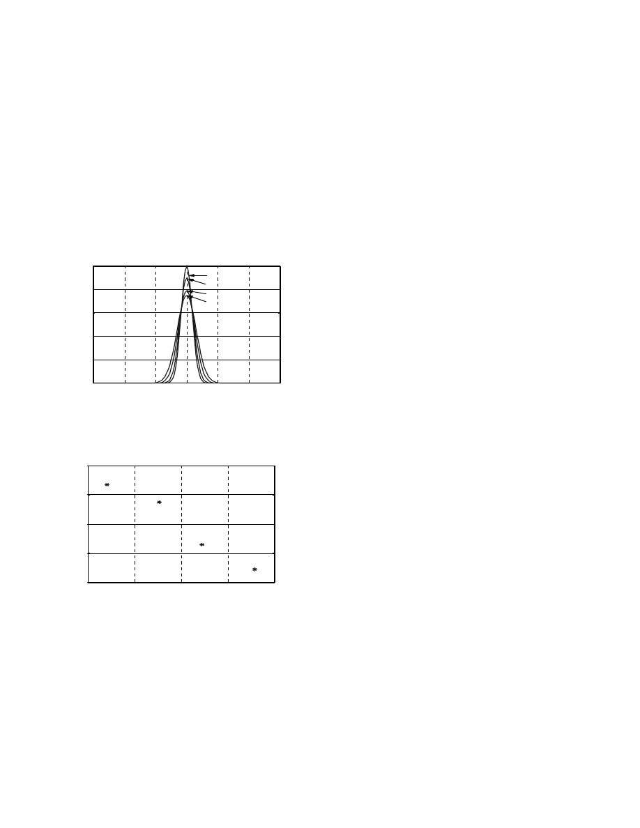
5.1 Wavelength Dependencies
The effect of quasi-monochromatic light was analyzed
for the optical system of Figure 4 at maximum reflectivity,
with T
plate
= 5.64
µ
m, T
gate
= 4.98
µ
m and T
air
=19.76
µ
m. As
shown in Figure 6 even when the light at
λ
0
=1.55
µ
m has a
0.02
µ
m distribution, the reflectivity remains almost
unchanged. However, beyond this bandwidth, the system
shows strong optical filter characteristics.
5.2 Dimensional Error Tolerance
Figure 7 shows the simplified representation of system
in Figure 4 which was used to model the dimensional errors.
Assume that the modulator is constructed for maximum
reflectivity, but the thickness T
air
has an offset of
δ
T. Under
the same design parameters as above (Figure 5), it is found
that the reflectivity is a periodic function of
δ
T. Figure 8
shows if the offset is in a range of 0 to 0.3
µ
m or in another
period, the variation of relative reflectivity is less than 1%.
The small change of reflectivity and its periodic property
provide high degree of freedom for design.
1 .5 3
1 .5 4
1 .5 5
1 .5 6
1 .5 7
0
0 .2
0 .4
0 .6
0 .8
1
W a v e l e n g t h ( m i c r o m e t e r s )
R
e
la
ti
v
e
R
e
fl
e
c
ti
v
ity
Figure 6: Reflectance wavelength dependencies
Fiber
Fiber
Fiber Core
Phase-
shifting gate
T
air
T
air
Light
Propagation
Direction
Figure 7: Schematic top view for error analysis with an
offset
δ
T of T
air
for maximum reflectivity situation
0
0 . 5
1
1 . 5
2
2 .5
3
3 . 5
4
0
0 . 2
0 . 4
0 . 6
0 . 8
1
O f f s e t o f T h i c k n e s s o f A i r G a p
Rel
at
iv
e r
e
fl
e
c
ti
vi
ty
Figure 8: The reflectivity variation due to the offset
δ
T
of the target thickness of T
air
δ
T
6 PERFORMANCE ANALYSIS
6.1 Beam Profile after Propagation
The propagation of light in the optical system is
modeled using the Beam Propagation Method (BPM) [10]
and encoded in Matlab. The beam profile emerging from
fiber 1 is treated as Gaussian distribution with
σ
0
= 5
µ
m for
a standard 10
µ
m optical fiber core. Under zero reflectivity
conditions, the final beam profiles at the input of fiber 2 for
different coupling distances with n
1
=1.467 (fiber core),
n
2
=1.0 (air), n
silicon
=3.5 (silicon) are given in Figure 9. If the
coupling distance between fibers is less than 40
µ
m, the
beam profiles have negligible distortion.
-6 0
-4 0
-2 0
0
2 0
4 0
6 0
0
0 .2
0 .4
0 .6
0 .8
1
B e a m w i d t h ( m i c r o m e t e r s )
B
e
a
m
P
ro
file
A t f ib e r 1
3 1 .2 m ic r o m e t e r s
4 8 .3 m ic r o m e t e r s
6 0 .7 m ic r o m e t e r s
Figure 9: The beam profiles before and after propagation
from fiber 1 to fiber 2 with different coupling
distance. T
gate
=3.54
µ
m and T
plate
= 1.0
µ
m are fixed
0 .5
1 .5
2 .5
3 .5
4 .5
-2 .5
-2 .3
-2 .1
-1 .9
-1 .7
G a t e T h i c k n e s s ( m i c r o m e t e r s )
In
ser
ti
o
n
l
o
ss (
d
B
)
Figure 10: The insertion loss and gate thickness relationship
6.2 Insertion Loss
The insertion loss of the optical system is shown in
Figure 10. Assume that the system is in the zero reflectivity
condition, the air gaps and the silicon buffer plates are both
fixed at odd multiples (55 for air gap and 9 for silicon plate)
of
λ
0
/4n, and T
gate
is even multiple of
λ
0
/4n
silicon
. Evidently,
the insertion loss increases with the gate thickness. When
the coupling distance reaches 47.47
µ
m and the gate
thickness is 2.88
µ
m, the insertion loss is about –2.2 dB.
7 CONCLUSIONS
Multi-objective optimization algorithm is demonstrated
for the optical design of an optical system with multiple
dimensional parameters. Beam propagating profiles and the
insertion loss are modeled using Beam Propagation Method.
Using these approaches a new micromechanical optical
modulator design using phase-shifting gate is proposed and
evaluated for the first time. It has a high modulation
efficiency of 99.5
%
, and the insertion loss can be easily kept
below –1.9 dB by reducing the coupling distance. The
device can be fabricated using standard micromachined
techniques. By integrating electrostatic microactuators on
the same chip, it is possible that the modulation speed of
this device can be upto 100 kHz.
REFERENCES
[1] W. H. Juan and S. W. Pang, “ High aspect ratio Si
vertical micromirror array for optical switch”, J.
Microelectromech. Syst., Vol(17), No.2, 1998, pp 207 –213
[2] Makoto Mita, et al, “Optical and surface
characterization of poly-si replica mirrors for an optical
fiber switch”, Transducers’99, pp 332-335
[3] S. S. Lee, E. Motamedi, and M. C. Wu, “Surface-
micromachined free-space fiber optic switches with
integrated microactuators for optical fiber communication
system”, Transducers’97, pp 85-88
[4] R. A. Miller, Y. C. Tai, G. Xu, J. Bartha, and F. Lin, “
An electromagnetic MEMS 2
×
2 fiber optic bypass switch”,
Transducers’97, pp 89-92
[5] C. Marxer, et al., “Vertical mirrors fabricated by
reactive ion etching for fiber optical switch applications,”
IEEE Int. Conf. On MEMS’97, pp 49-54
[6] D. E. Aspnes, “Optical functions of intrinsic silicon:
table of refractive index, extinction coefficient and
absorption coefficient vs energy (0 to 400eV)”, in
Properties of Silicon, Emis Data Reviews Series No.4 (IEE,
London 1988), Sect. 2.6, pp. 72-79
[7] Y. Uenish, M. Tsugai and M. Mehregany, “Micro-opto-
mechanical devices fabricated by anisotropic etching of
(110) silicon”, J. Micromech. Microeng., 1995, pp 305-312
[8] L. Que, J. Park and Y. Gianchandani, “A bent beam
electro-thermal actuator with high force application,” IEEE
Int. Conf. On MEMS’99, pp 31-36
[9] W.C. Tang, T. U. Chong, H. Nguyen, and R. T. Howe,
“Laterally driven polysilicon resonant microstructures,”
Sensors and Actuators, V. 20, 1987, pp.25-32
[10] Born and Wolf, Principles of Optics, 4
th
edition,
Pergamon press, 1970. Pollock, Fundamentals of
Optoelectronics, R. D. IRWIN, INC., 1995
[11] MATLAB 5.3 User’s Guide (1995)
Wyszukiwarka
Podobne podstrony:
Design and construction of three phase transformer for a 1 kW multi level converter
PROPAGATION MODELING AND ANALYSIS OF VIRUSES IN P2P NETWORKS
Modeling And Simulation Of ATM Networks
Multiscale Modeling and Simulation of Worm Effects on the Internet Routing Infrastructure
Properties and Structures of Three phase PWM AC Power Controllers
Modeling and Control of an Electric Arc Furnace
An investigation of shock induced temperature rise and melting of bismuth using high speed optical p
Design Guide 02 Design of Steel and Composite Beams with Web Openings
[Raport] Roundabouts and Safety for Bicyclists Empirical Results and Influence of Difference Cycle F
Modeling and minimizing process time of combined convective and vacuum drying of mushrooms and parsl
Design and implementation of Psychoacoustics Equalizer for Infotainment
Eurocode 6 Part 2 1996 2006 Design of Masonry Structures Design Considerations, Selection of Mat
Eurocode 8 Part 1 1998 2004 Design of Structures for Earthquake Resistance General Rules Seism
The Discrete Time Control of a Three Phase 4 Wire PWM Inverter with Variable DC Link Voltage and Bat
Eurocode 2 Part 3 2006 UK NA Design of concrete structures Liquid retaining and containing struc
The Discrete Time Control of a Three Phase 4 Wire PWM Inverter with Variable DC Link Voltage and Bat
Eurocode 8 Part 5 1998 2004 Design of Structures for Earthquake Resistance Foundations, Retaini
więcej podobnych podstron