Winstar Display describes here how to use Graphic LCD modules.
A
s we enter the technological era of the
world, many gadgets, devices,
appliance, equipments etc. are
evolving. And beyond that evolution, as
a person, as a human; the one who
controls this computer world of us, must know how
to employ it of course.
That's why Winstar Display Co., Ltd. is here to give
knowledge of what technology is all about to
sustain life. As the vision of our company goes:
WIN your life; STAR your eyes. So with that, it is a
great privilege for us to give information about our
product, especially on how to use graphic LCD
modules for the benefits of everybody.
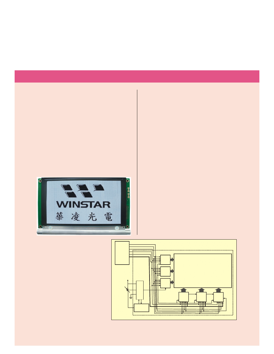
So let's see the Winstar product WG240128B as an
example.
The whole picture is composing of 240
dots/pixel/character column and 128
dots row as shown to the above photo.
But before the whole picture shows, it
takes some process first. And that is the
responsibility of the controller of every
module. This controller will be the one
to give signals to the whole module.
The different signals are below:
Ç
CP Signal
From the picture, this is the foundation
of everything, of the whole image. This
Control Signals
represents the single dot or single pixel or single
character of the picture.
Ç
LP Signal
This is the one that responsible to change another
line if CP Signal occupies the whole row. This is the
one that tells the CP to take another line.
Ç
FLM Signal
As the LP Signal finishes its responsibility to tell CP to
change the line, FLM will be the one to tell LP to
change its page if the line is almost done. So this is
the one responsible for the whole page.
Ç
M Signal
As the character, the line and the page are almost
done, M Signal takes place by telling the BIAS to
change its voltage so that the LCD (the nematic
itself) will turn or change.
As we know now how each dot in every line and in
every page occur, let us see now what is behind on
every graphic LCD.
So as you can see the illustration, before all the dots
in every line and in every page takes place, there is
different process that happens first. The whole
picture itself comes from the signal of its
COMMON and SEGMENT IC (Integrated Chip)
that builds the row and column of every character.
Block Diagram of LCD Module
COURTESY BY WINSTAR DISPLAY
How to Use a Graphic LCD
[
]
DISPLAY
WG240128A
CL2(CP)
CL1(LP)
M
FLM
DISPOFF
DBO-DB3
CONTROLLER
COM
1-80
Drives
COM
81-160
Drives
COM
161-128
Drives
SIG 1-80
Drives
SIG
81-160
Drives
SIG
161-240
Drives
Eds
240x128 DOT
Bias
and
Power
circuit
N-V
Genrator
Where in fact, asks their signal from its
CONTROLLER and its proper voltages from the
BIAS Circuit that will be acted upon by the Negative
Voltage Generator to avoid some shortages and
burning of other components IC.
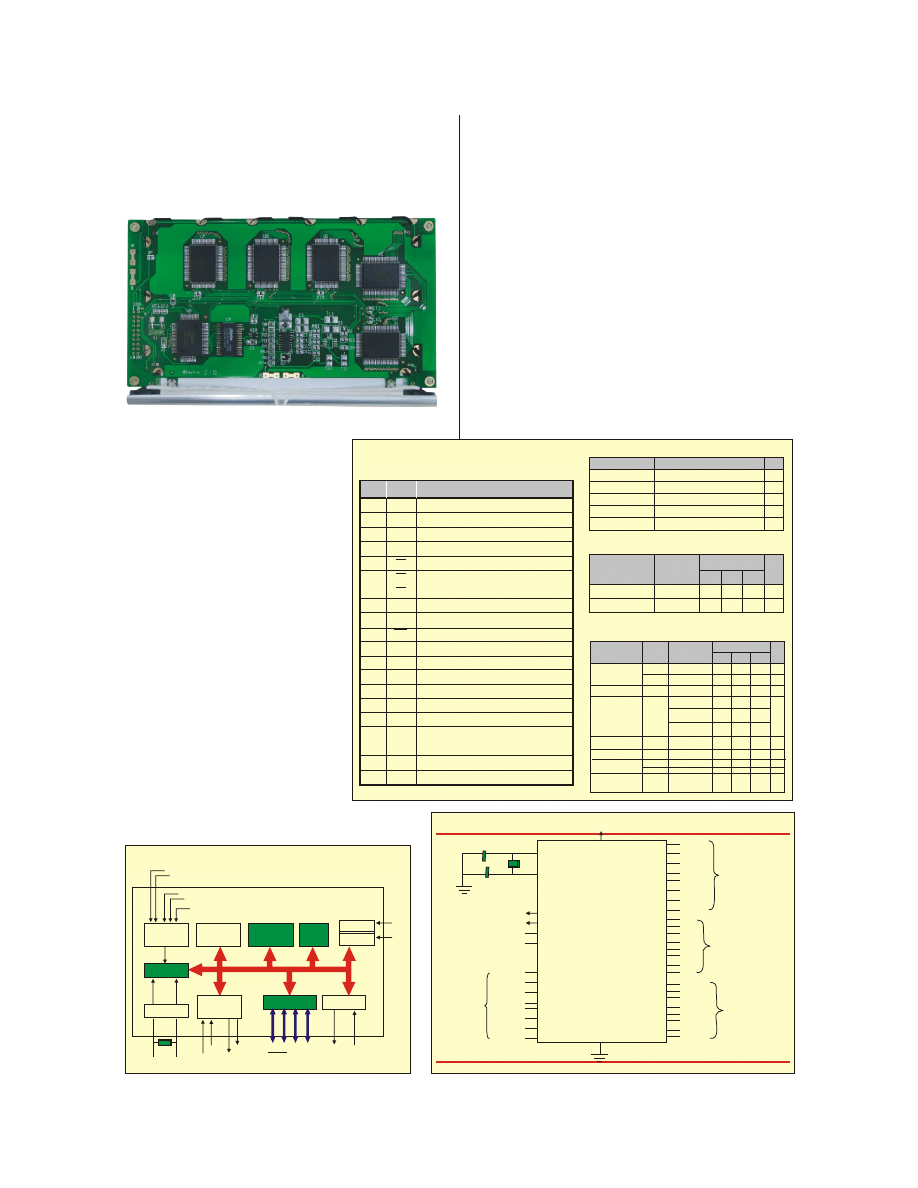
Aside from the circuitry of the LCD
Module, we need also to learn
about on how we are going to
make real the picture that we want
to pop up on the screen itself. How
a single character can be put on the
actual figure.
First thing we need to find out is the
data bus IC (microprocessor) that
we are going to use to make the
program that will be use on the
module. This will be the foundation
of all the data that we want to put on
the module that we want to utilize
and of course we will base our
program on the type of data bus IC
that we use.
Winstar Display Co., Ltd. is
commonly using the 8051
Controller and 8051 IC
Application
microprocessor of Intel and uses the C Language
for its program. This is where we format the entire
program that we are using for the different
applications of our modules, depending on the
capacity of its application.
Winstar takes time also in choosing the accurate
Controller IC of the module depending on the
function of the LCD or the request of its customer.
Programs can be created as we comprehend on the
specification of the controller IC that we are using.
From that specification, we can know the correct
interface of it to its Data Bus and the correct way on
how to program and apply the controller.
So with the Controller and Data Bus IC connection,
we can now create all the thoughts that we want to
be view on our screen.
Let us take a look the sample module of
Printed Circuit Board of WG240128A
8051 Block Diagram
INT1
INT2
Note: bold-faced pin assignments for P1 and P3.
Timer 1
Timer 0
Serial Port
Serial Port
Interrupt
Control
Other
Registers
T1
T0
Oscillator
Bus
Control
EA
RST
PSEN
ALE
P0 P1 P2 P3
TXD RXD
Address / Data
128 B
RAM
4KB
ROM
Timer 1
Timer 0
CPU
I/O ports
[
]
DISPLAY
8051
30pF
30pF
(29)
(30)
(31)
(9)
PSEN
ALE
EA
RST
RD(17)
WR(16)
T1(15)
T0(14)
INT(13)
INT(12)
TXT(11)
RXD(10)
P3.7
P3.6
P3.5
P3.4
P3.3
P3.2
P3.1
P3.0
AD7(32)
AD6(33)
AD5(34)
AD4(35)
AD3(36)
AD2(37)
AD3(38)
AD0(39)
Port 0
P0.7
P0.6
P0.5
P0.4
P0.3
P0.2
P0.1
P0.0
P1.7
P1.6
P1.5
P1.4
P1.3
P1.2
P1.1
P1.0
(8)
(7)
(6)
(5)
(4)
(3)
(2)
(1)
A15(28)
A14(27)
A13 (26)
A12 (25)
A11 (24)
A10 (23)
A9 (22)
A8(21)
Port 1
Port 2
P2.7
P2.6
P2.5
P2.4
P2.3
P2.2
P2.1
P2.0
Port 3
VSS(20)
VCC(40)
XTL1 (19)
XTL2 (18)
8051 Pinouts
Pin
No
Symbol
Function
1
2
3
4
5
6
7
8
9
10
11
12
13
14
15
16
17
18
19
20
FGND
VSS
VDD
VO
WR
RD
CE
C/D
NC/VEE
RST
DB0
DB1
DB2
DB3
DB4
DB5
DB6
DB7
FS
RV
Frame GEN (connected to bezel)
GND
Power Supply for logic circuit
Contrast Adjustment
Data write
Data road
Chip enable
Code/Data
No connect on/ Negative Voltage output
Controller reset
Data bus line
Data bus line
Data bus line
Data bus line
Data bus line
Data bus line
Data bus line
Data bus line
Font Selection
Reverse
FS="H", 6x8 character font
FS="L", 8x8 character font
Feature
1. Built-in controler TOSHIBA-(TE963C)
2. 1/128 duty cycle
3. Built -in N/V (Option)
Module Dimension
Viewing Area
Dot Size
Dot Pitch
Mounting hole
Mechanical Data
Item
Standard Value
Unit
mm
mm
mm
mm
mm
170.0x103.5
132.0x76.0
0.47x0.47
0.5x0.5
162.0x85.0
Absolute Maximum Rating
Item
Symbol
Unit
Standard Value
min. typ. max.
4.75 5.0 5.25 v
-0.3 - VDD V
Power Supply
Input Voltage
VDD-VSS
VI
Note:VSS=0 Volt, VDD=5.0 Volt.
Electronical Characteristics
Item
Symbol
Input Voltage
Supply Current
VDD
VIO
IDD
VDD-V0
VF
IF
IF
IEL
LED Forward Voltage
LED Forward Current
CCFL
EL
Condition
L Leve
H Level
VDD=5.0V
0
-20 C
0
25 C
0
70 C
0
25 C
0
25 C
0
25 C
Vel=110V/AC,
400Hz
Standard Value
Unit
min. typ. Max.
0.7VDD
-
-
19.1
18.1
17.1
-
-
-
-
V
V
mA
V
V
mA
mA
mA
VDD
0.3VDD
-
20.1
19.1
18.1
-
-
0.0
5.0
-
-
23
19.5
18.5
17.5
-
-
VF
0
25 C
-
V
580
325
-
-
Recommended LC
Driving Voltage for
Normal Temp.
Version module
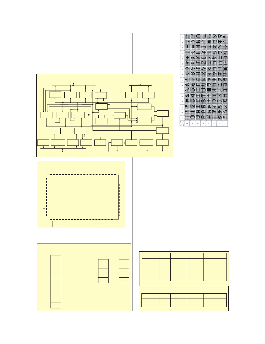
WG240128A on how we really create this one.
With the following feature, we can start. As we are
aware of its controller, we need to study it for the
connection and programming.
TOSHIBA T6963C
RAM Interface
The external RAM is
u s e d t o s t o r e
display data (text,
g r a p h i c a n d
external CG data).
With single-scan,
text data, graphic
data and external CG data
can be freely allocated to the memory
With dual scan, LCD I is allocated to 0000H to
7FFFH (32 KB max), LCD II is allocated to 8000H
to FFFFH (32 KB max). Text data, graphic data and
external CG data can be freely allocated in LCD I.
In LCD II, the same addresses must be allocated as
in LCD I, except ad15.ad15 determines selection of
LCD I or LCD II. It can be use the address decoded
signals ce0 (0000 to 07FFH), ce1 (0800 to 0FFFH)
within 4KB. ce0 and ce1 allow decoding of
addresses in the ranges (0000 to 07FFH) and
(0800 to 0FFFH) respectively within a 4-KB
memory space.
To completely create a program that will be use on
the LCD module application, we need also to take
note of the following:
Text
Area
Graphic
Area
CG RAM
Area
0000H
3FFFH
77FFH
7FFFH
Text
Area
Graphic
Area
CG RAM
Area
8000H
BFFFH
F7FFH
FFFFH
(2) Dual-Scan
CG : Character Generator
(Example)
(1) Single-Scan
Text
Area
Graphic
Area
CG RAM
Area
0000H
7FFFH
F7FFH
FFFFH
[
]
DISPLAY
ad0 to ad15 (To/From RAM)
d0 to d7 (To / From RAM)
Text
Pointer
Graphic
Pointer
Address
Pointer
CG
Register
Ram Data
Latch
Ram Data
Buffer
CG Rom
Graphic
Data Latch
Copy
Control
Internal
Ram
Arithmetic
Circuit
Cursor
Pointer
Cursor
Control
Text
Data Latch
Display
Selector
Address
control
Data
Control
Serializer
Status
Suffar
Instruction
Latch
Data
Latch
Data
Buffer
Data
Stack
osc
Timing
Control
LCD Timing
Generator
LCD Data
Control
D0 to D7 (To/ From CPU)
CDATA, LP, FR,
HSCP, LSCP
X1
X0
ED, HOD, LOD
Block Diagram
55
56
57
58
59
60
61
62
63
64
65
66
67
32
31
30
29
28
27
26
25
24
23
22
54 53 52 51 50 49 48 47 46 45 44 43 42 41 40 39 38 37 36 35 34 33
1 2 3 4 5 6 7 8 9 10 11 12 13 14 15 16 17 18 19 20 21
LP
CDATA
FR
CH1
CH2
DSOPN
VDD
SDSEL
VSS
T2
T1
XI
X0
ec
r/w
d7
d6
d5
Vd0
d4
d3
d2
d1
d0
Pin Assignment
H
A
L
T
R
E
S
E
T
M
D
S
M
D
0
M
D
1
M
D
2
M
D
3
F
5
0
F
5
1
D
0
D
1
D
2
D
3
D
4
D
5
D
6
D
7
W
R
R
D
C
E
C
/D
D
U
A
L
H
S
C
P
E
D
H
O
D
c
0
1
c
0
a
d
1
5
a
d
1
4
a
d
1
3
a
d
1
2
a
d
1
1
a
d
1
0
a
d
9
a
d
8
a
d
7
a
d
6
a
d
5
a
d
4
a
d
3
a
d
2
a
d
1
a
d
0
T6963C
(TOP VIEW)
T
h
e
r
e
la
ti
o
n
b
e
tw
e
e
n
c
h
a
ra
c
te
r
c
o
d
e
s
a
n
d
c
h
a
ra
c
te
r
p
a
tt
e
rn
(
C
G
R
O
M
T
y
p
e
0
2
0
1
)
Note: All of the information can
be comprehend by reading all
the specifications of the said
controller. So if we know that,
we can now go on to
programming itself.
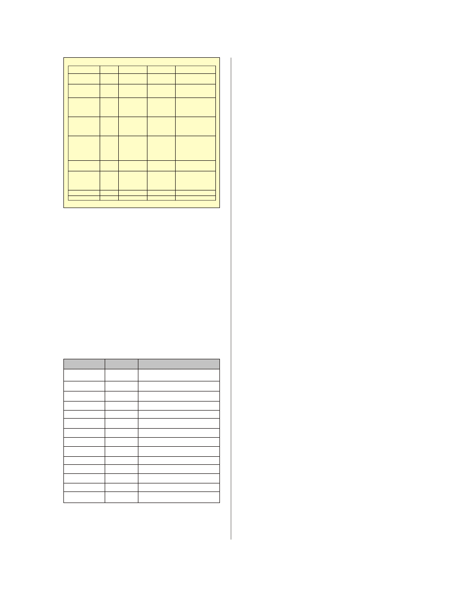
Command
Code
D1
D2
Funcation
11110XXX
11111XXX
1111X000
1111X001
1111X010
1111X011
1111X100
1111X101
1111X110
1111X111
-
-
-
-
-
-
-
-
-
-
-
-
-
-
-
-
-
-
-
-
Bit Set/ Reset
Bit Reset
Bit Set
Bit 0 (LSB)
Bit 1
Bit 2
Bit 3
Bit 4
Bit 5
Bit 6
Bit 7 (MSB)
Code
Hex.
D1
D1
Funcation
21H
22H
24H
Set Cursor Pointer
Set Offset Register
Set Address Pointer
X ADRS
DATA
LOW ADRS
00100001
00100010
00100100
Y ADRS
00H
HIGH ADRS
Setting registers
X:invalid
Creating A Program
Before we actually make a program, lets first take
note the port of our microprocessor for connections
and compatibility.
So with that, basic knowledge of C language is an
important tool so we can go with the flow of the
programming. Different operations must be
applied such as the +, -, *, /, %, ++, --, >, <,
<=, >=, &, ^, ~, >>, << , !, !=, ==. And of
course some programming instructions such as the
loop instructions ( for, while and do while),
switching instructions, array, string, etc.
VARIABLE DATA TYPE:
This one is very important to think of.
SAMPLE GRAPHIC PROGRAM
#include
<reg51.h>
#include
<INTRINS.>
#define DATA_BUS
P1
sbit
LCM_FS
= P3^1;
sbit
LCM_MD2 = P3^2;
sbit
LCM_RESET
= P3^3;
sbit
LCM_CE
= P3^4;
sbit
LCM_WR
= P3^6;
sbit
LCM_RD
= P3^7;
unsigned
char
code
picture [1 2 8 ]
[30] = note: code of the picture can be put in here.
void write_command (unsigned char par_1)
{
LCM_CD
=
1;
LCM_CE
=
0;
LCM_WR
=
0;
_nop_();
_nop_();
DATA_BUS
=
par_1;
_nop_();
_nop_();
LCM_CE
=
1;
LCM_WR
=
1;
}
void write_data (unsigned char par_1)
{
LCM_CD = 0;
LCM_CE = 0;
LCM_WR = 0;
_nop_();
_nop_();
DATA_BUS = par_1;
_nop_();
_nop_();
LCM_CE = 1;
LCM_WR =1;
}
void init_T6963C ()
{
LCM_RESET = 0;
_nop_();
_nop_();
_nop_();
LCM_RESET = 1;
_nop_();
_nop_();
_nop_();
LCM_MD2 = 1;
LCM_FS = 0;
write_data (0x00);
write_data (0x00);
write_command(0x40);
write_data (0x00);
write_data (0x02);
[
]
DISPLAY
Command
Code
D1
D2
Funcation
00100001
00100010
00100100
Register Setting
Set Control Word
01000000
01000001
01000010
01000011
Mode Set
1000X000
1000X001
1000X011
1000X100
10000XXX
10001XXX
Display Mode
10010000
1001XX10
1001XX11
100101XX
100110XX
100111XX
Cursor Pattern Select
10100000
10100001
10100010
10100011
10100100
10100101
10100110
10100111
X Address
Data
Low Address
Y Address
00H
High Address
Set Cursor Pointer
Set Offset Register
Set Address Pointer
Low Address
Columns
Low Address
Columns
High adress
00H
High address
00H
-
-
-
-
-
-
-
-
-
-
-
-
-
-
-
-
-
-
-
-
-
-
-
-
-
-
-
-
-
-
-
-
-
-
-
-
-
-
-
-
-
-
-
-
-
-
-
-
-
-
-
-
-
Set Text Home address
Set Text Area
Set Graphic Home Address
Set Graphic Area
OR Mode
ExOR Mode
ANO mode
Text Attribute mode
Internal CG ROM mode
External CG RAM mode
Display Off
Cursor On , blink Off
Cursor on Bilk on
Text on. graphic off
Text off. graphic on
Text on. graphic on
1-line cursor
2-line cursor
3-line cursor
4-line cursor
5-line cursor
6-line cursor
7-line cursor
8-line cursor
Data Auto Read/ Write
Data Read / Write
10110000
10110001
10110010
Set Data Auto Write
Set Data Auto Read
Auto Reset
Data Write and increment ADP
Data Read and increment ADP
Data Read and Drecrement ADP
Data Read and Drecrement ADP
Data Write and Nonvariable ADP
Data Read Nonvariable ADP
11000000
11000001
11000010
11000011
11000100
11000101
Data
-
Data
-
Data
-
-
Screen Peek
Screen Peek
Screen Copy
Screen Copy
Command Definitions
X:invalid
11100000
11101000
bit
signed char
unsigned char
enum
signed short
unsigned short
signed int
unsigned int
signed long
unsigned long
float
sbit
sfr
sfr16
DATA TYPE
BITS BYTES
VALUE RANGE
1
8
8
16
16
16
16
16
32
32
32
1
8
16
0~1
(-)128 ~ (+)127
0 ~ 255
(-) 32768 ~ (+)32767
(-) 32768 ~ (+)32767
0 ~ 65535
(-) 32768 ~ (+) 32767
0 ~ 65535
(-)2147483648 ~ (+)2147483648
0 ~ 4294967295
0.175494E-38 ~ 0.402823E+38
0~1
0 ~ 255
0 ~ 65535

write_command(0x42);
write_data (0x1E);
write_data (0x00);
write_command(0x41);
write_data (0x1E);
write_data (0x00);
write_command(0x43);
write_command (0x80);
write_command (0x98);
}
void clear ()
{
unsigned char i, j;
write_data (0x00);
write_data (0x20);
write_command (0x24);
write_command (0xB0);
for ( i=0; i<=128; i++)
{
for (j=0; j<=30; j++)
{
write_data (0x55);
}
}
write_command (0xB2);
}
void fill_screen (picture)
char picture [128] [30];
{
unsigned char i, j;
write_data (0x00);
write_data (0x20);
write_command (0x24);
}
void main ()
{
init_T6963C ();
clear ();
fill_screen (picture1);
while ();
{
}
}
With these article, hope it would be a great help for
the user who wants to be aware of using the
Graphic LCD Module. If you need further
information, please contact with Winstar Display
Co. Ltd., Web : www.winstar.com.tw
[
]
DISPLAY
Document Outline
Wyszukiwarka
Podobne podstrony:
How to Use a Graphic LCD id 206 Nieznany
How to Use Linked In
how to use toyota lexus smart key programmer
EWD How to Use this Manual
How to Use the Electrical Wiring Diagram
How to Use RGB LEDs Backlight o Nieznany
How to use blush, Moda-Uroda
how to use fvdi fwdownloader fiat
How to use software of Ethernet packet?pture to?pture WAN port packets
how to use the flash tool for Xperia
! Martial Arts How To Use Tai Chi As A Fighting Art (Erle Montaigue)
EWD How to Use this Manual
how to use fgtech with bdm function
How to use Award WinFlash utility
How to Use the Overall EWD
How to Use Linked In
how to use toyota lexus smart key programmer
więcej podobnych podstron