This document contains information on a new product. Specifications and information herein are subject to change without notice.
© Motorola, Inc., 2003
HCS12DBFAMILYPP/D
Rev. 0.7, 8/2003
HCS12DB Family Product
Proposal
Product Proposal
Introduction
Designed for automotive multiplexing applications, members of the
MC9S12DB-Family of 16 bit Flash-based microcontrollers are fully pin
compatible and enable users to choose between different memory and
peripheral options for scalable designs. All MC9S12DB-Family members are
composed of standard on-chip peripherals including a 16-bit central processing
unit (CPU12), up to 128K bytes of Flash EEPROM, 8K bytes of RAM, 2K bytes
of EEPROM, two asynchronous serial communications interfaces (SCI), up to
two serial peripheral interfaces (SPI), an enhanced capture timer (ECT), two 8-
channel, 10-bit analog-to-digital converters (ADC), an eight-channel pulse-
width modulator (PWM), Byteflight interface and up to two CAN 2.0 A, B
software compatible modules (MSCAN12). System resource mapping, clock
generation, interrupt control and bus interfacing are managed by the system
integration module (SIM). The MC9S12DB-Family has full 16-bit data paths
throughout, however, the external bus can operate in an 8-bit narrow mode so
single 8-bit wide memory can be interfaced for lower cost systems. The
inclusion of a PLL circuit allows power consumption and performance to be
adjusted to suit operational requirements. In addition to the I/O ports available
in each module, up to 22 I/O ports are available with Wake-Up capability from
STOP or WAIT mode.
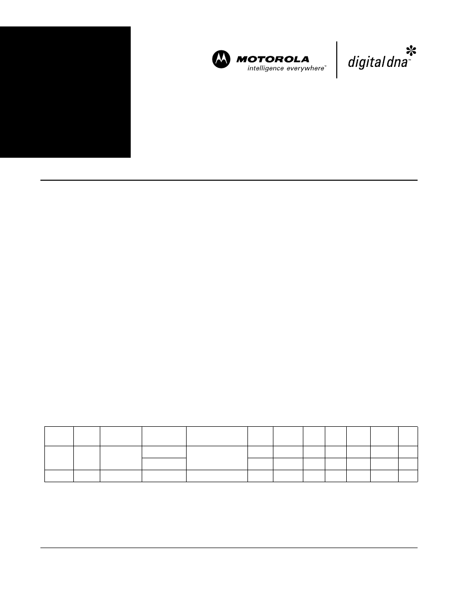
Table 1. MC9S12DB Family Members
Flash
RAM
EEPROM
Package
Device
CAN
Byte
Flight
SCI
SPI
A/D
PWM
I/O
128K
8K
2K
112 LQFP
MC9S12DB128
2
1
2
2
2/16
8 ch
91
80 QFP
0
1
1
2
1/8
7 ch
59
64K
8K
2K
80 QFP
MC9S12DB64
0
1
1
1
1/8
7 ch
59

HCS12DBFAMILYPP/D
2
HCS12DB Family Product Proposal
MOTOROLA
Features
NOTE:
Not all features listed here are available in all configurations.
•
16-bit CPU12
–
Upward compatible with M68HC11 instruction set
–
Interrupt stacking and programmer’s model identical to M68HC11
–
20-bit ALU
–
Instruction queue
–
Enhanced indexed addressing
•
Multiplexed bus
–
Single chip or expanded
–
16 address/16 data wide or 16 address/8 data narrow modes
–
External address space 1 MB for data and program space (112 pin
package only)
•
Wake-up interrupt inputs depending on the package option
–
8-bit port H
–
4-bit port J
–
8-bit port shared with PWM/SPI
•
Memory options
–
64K, 128K Byte Flash EEPROM
–
2K Byte EEPROM
–
8K Byte RAM
•
One or Two analog-to-digital converters (ATD)
–
1 or 2 times 8-channels, 10-bit resolution depending on the package
option
–
External conversion trigger capability
•
Up to two 1 M bit per second, CAN 2.0 A, B software compatible
modules
–
Five receive and three transmit buffers
–
Flexible identifier filter programmable as 2 x 32 bit, 4 x 16 bit or
8 x 8 bit
–
Four separate interrupt channels for Rx, Tx, error and wake-up
–
Low-pass filter wake-up function
–
Loop-back for self test operation
•
Enhanced Capture Timer (ECT)
–
16-bit main counter with 7-bit prescaler
–
8 programmable input capture or output compare channels; 4 of the
8 input captures with buffer
–
Input capture filters and buffers, three successive captures on four
channels, or two captures on four channels with a capture/compare
selectable on the remaining four
–
Four 8-bit or two 16-bit pulse accumulators
–
16-bit modulus down-counter with 4-bit prescaler
–
Four user-selectable delay counters for signal filtering

HCS12DBFAMILYPP/D
Features
MOTOROLA
HCS12DB Family Product Proposal
3
•
Seven or eight PWM channels with programmable period and duty cycle
–
8-bit 4-channel or 16-bit 2-channel (80-Pin Version)
–
8-bit 8-channel or 16-bit 4-channel (112-Pin Version)
–
Separate control for each pulse width and duty cycle
–
Center- or left-aligned outputs
–
Programmable clock select logic with a wide range of frequencies
•
Serial interfaces
–
Two asynchronous serial communications interfaces (SCI)
–
Up to two synchronous serial peripheral interfaces (SPI)
•
Byteflight
–
10 MBit/s serial protocol
•
SIM (system integration module)
–
CRG (windowed COP watchdog, real-time interrupt, clock monitor,
clock generation and reset)
–
MEBI (multiplexed external bus interface)
–
MMC (memory map and interface)
–
INT (interrupt control)
–
BKP (breakpoints)
–
BDM (background debug mode)
•
Clock generation
–
Phase-locked loop clock frequency multiplier
–
Limp home mode in absence of external clock
–
Slow mode divider
–
Low power 0.5 to 40 MHz crystal oscillator reference clock
•
Operating frequency
–
50 MHz equivalent to 25 MHz bus speed for single chip
–
40 MHz equivalent to 20 MHz bus speed in expanded bus modes
•
Internal 5 V to 2.5 V regulator
•
112-Pin LQFP or 80-Pin QFP package
–
I/O lines with 5-V input and drive capability
–
5-V ATD inputs
–
Dual supply (5 V for I/O and ATD, 2.5 V for logic
•
Development support
–
Single-wire background debug™ mode (BDM)
–
On-chip hardware breakpoints
HCS12DBFAMILYPP/D
4
HCS12DB Family Product Proposal
MOTOROLA
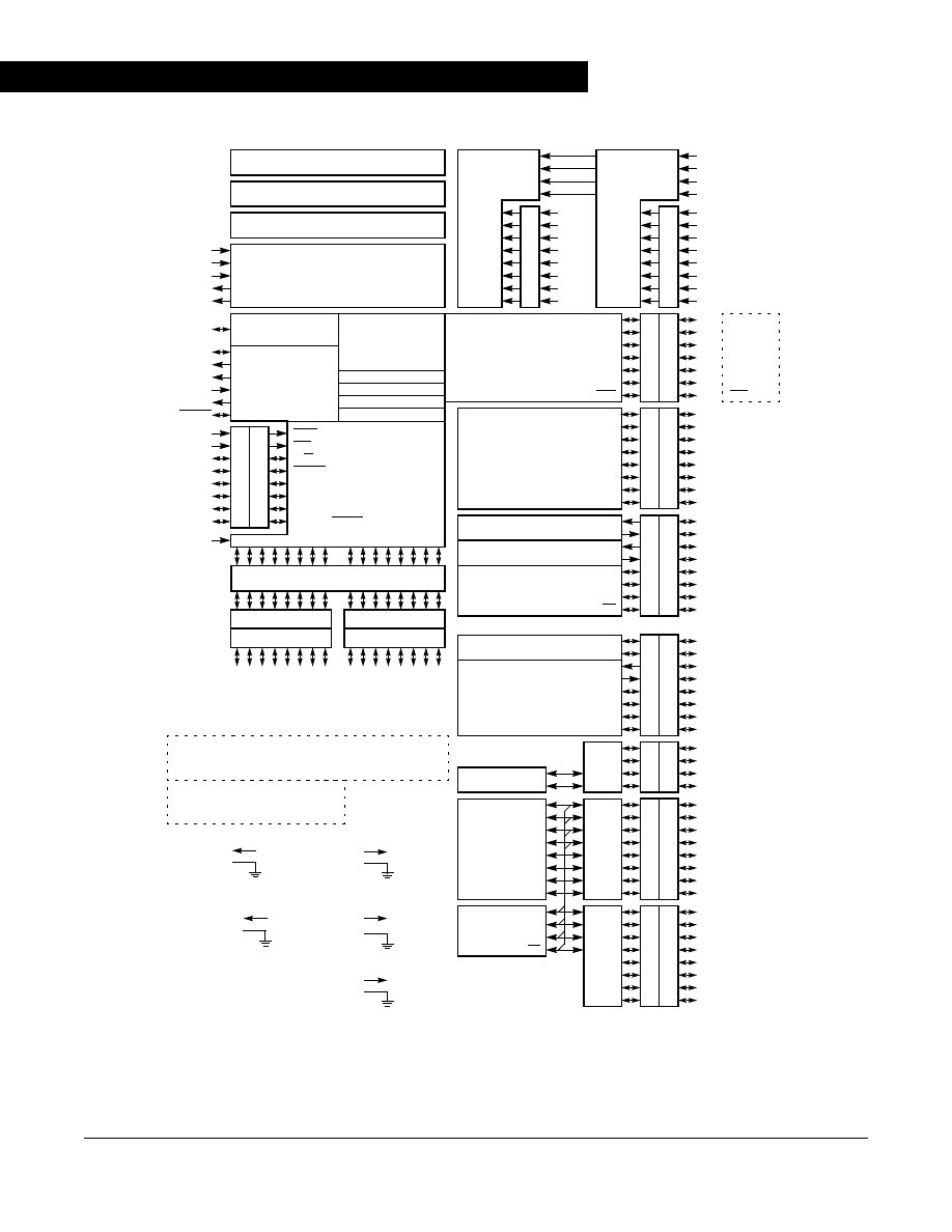
Figure 1. MC9S12DB Family Block Diagram
64K or 128K Byte Flash EEPROM
8K Byte RAM
Enhanced Capture
RESET
EXTAL
XTAL
V
DD1,2
V
SS1,2
SCI0
2K Byte EEPROM
BKGD
R/W
MODB
XIRQ
NOACC/XCLKS
System
Integration
Module
(SIM)
V
DDR
CPU12
Periodic Interrupt
COP Watchdog
Clock Monitor
Single-wire Background
Breakpoints
PLL
V
SSPLL
XFC
V
DDPLL
Multiplexed Address/Data Bus
VDDA
VSSA
VRH
VRL
ATD0
Multiplexed
Wide Bus
Multiplexed
V
DDX
V
SSX
Internal Logic 2.5V
Narrow Bus
PPAGE
V
DDPLL
V
SSPLL
PLL 2.5V
IRQ
LSTRB
ECLK
MODA
PA
4
PA
3
PA
2
PA
1
PA
0
PA
7
PA
6
PA
5
TEST
AD
DR1
2
AD
DR1
1
AD
DR1
0
AD
DR9
AD
DR8
AD
DR1
5
AD
DR1
4
A
DDR
13
DA
T
A
1
2
DA
T
A
1
1
DA
T
A
1
0
DA
T
A
9
DA
T
A
8
DA
T
A
1
5
DA
T
A
1
4
DA
T
A
1
3
PB4
PB3
PB2
PB1
PB0
PB7
PB6
PB5
AD
DR4
AD
DR3
AD
DR2
AD
DR1
AD
DR0
AD
DR7
AD
DR6
AD
DR5
DA
T
A
4
DA
T
A
3
DA
T
A
2
DA
T
A
1
DA
T
A
0
DA
T
A
7
DA
T
A
6
DA
T
A
5
DA
T
A
4
DA
T
A
3
DA
T
A
2
DA
T
A
1
DA
T
A
0
DA
T
A
7
DA
T
A
6
DA
T
A
5
PE3
PE4
PE5
PE6
PE7
PE0
PE1
PE2
AN2
AN6
AN0
AN7
AN1
AN3
AN4
AN5
PAD03
PAD04
PAD05
PAD06
PAD07
PAD00
PAD01
PAD02
IOC2
IOC6
IOC0
IOC7
IOC1
IOC3
IOC4
IOC5
PT3
PT4
PT5
PT6
PT7
PT0
PT1
PT2
V
RH
V
RL
VDDA
VSSA
VRH
VRL
ATD1
AN2
AN6
AN0
AN7
AN1
AN3
AN4
AN5
PAD11
PAD12
PAD13
PAD14
PAD15
PAD08
PAD09
PAD10
V
DDA
V
SSA
RXD
TXD
MISO
MOSI
PS3
PS4
PS5
PS0
PS1
PS2
SCI1
RXD
TXD
PWM2
PWM6
PWM0
PWM7
PWM1
PWM3
PWM4
PWM5
PP3
PP4
PP5
PP6
PP7
PP0
PP1
PP2
PIX2
PIX0
PIX1
PIX3
ECS
PK3
PK7
PK0
PK1
XADDR17
ECS
XADDR14
XADDR15
XADDR16
SCK
SS
PS6
PS7
SPI0
PJ6
PJ7
CAN0
RxCAN
TxCAN
PM1
PM0
PM2
PM3
PM4
PM5
PM6
PM7
KWH2
KWH6
KWH0
KWH7
KWH1
KWH3
KWH4
KWH5
PH3
PH4
PH5
PH6
PH7
PH0
PH1
PH2
KWJ0
KWJ1
PJ0
PJ1
I/O Driver 5V
V
DDA
V
SSA
A/D Converter 5V &
DDRA
DDRB
PTA
PTB
DD
RE
PTE
AD1
AD0
PTK
DD
RK
PTT
D
DRT
PTP
DD
RP
PTS
DD
RS
PTM
DD
RM
PTH
DD
RH
PTJ
DD
RJ
PK2
Clock and
Reset
Generation
Module
Voltage Regulator
V
SSR
Debug Module
V
DD1,2
V
SS1,2
VREGEN
V
DDR
V
SSR
Voltage Regulator 5V & I/O
Not all functionality shown in this
block diagram is available in all versions.
CAN4
RxCAN
TxCAN
MISO
MOSI
SCK
SS
SPI1
PIX4
PIX5
PK4
PK5
XADDR18
XADDR19
Voltage Regulator Reference
KWP2
KWP6
KWP0
KWP7
KWP1
KWP3
KWP4
KWP5
KWJ6
KWJ7
Timer
Signa
ls sh
ow
n in
Bold
a
re
no
t a
vaila
bl
e o
n
th
e
80
Q
F
P
P
ac
ka
ge
RX_BF
TX_BF
BYTEFLIGHT
BF_PSYN
BF_PROK
BF_PERR
BF_PSLM
PWM

HCS12DBFAMILYPP/D
Pin Out Explanations:
MOTOROLA
HCS12DB Family Product Proposal
5
Pin Out Explanations:
•
A/D is the number of modules/total number of A/D channels.
•
I/O count:
–
112 Pin Package:
–
Port A = 8, B = 8, E = 6 + 2 input only, H = 8, J = 4, K = 7, M = 8,
P = 8, S = 8, T = 8,
–
PAD = 16 input only.
–
22 inputs provide Interrupt capability (H =8, P= 8, J = 4, IRQ,
XIRQ)
–
80 Pin Package:
–
Port A = 8, B = 8, E = 6 + 2 input only, M = 6, P = 7, S = 6, T =
8, PAD = 8 input only
–
9 inputs provide Interrupt capability (P= 7, IRQ, XIRQ)
•
MC9S12DB64 features only one SPI, SPI0
•
SPI1 pins are shared with PWM3:0 or Port H3:0 routeable under
software control
HCS12DBFAMILYPP/D
6
HCS12DB Family Product Proposal
MOTOROLA
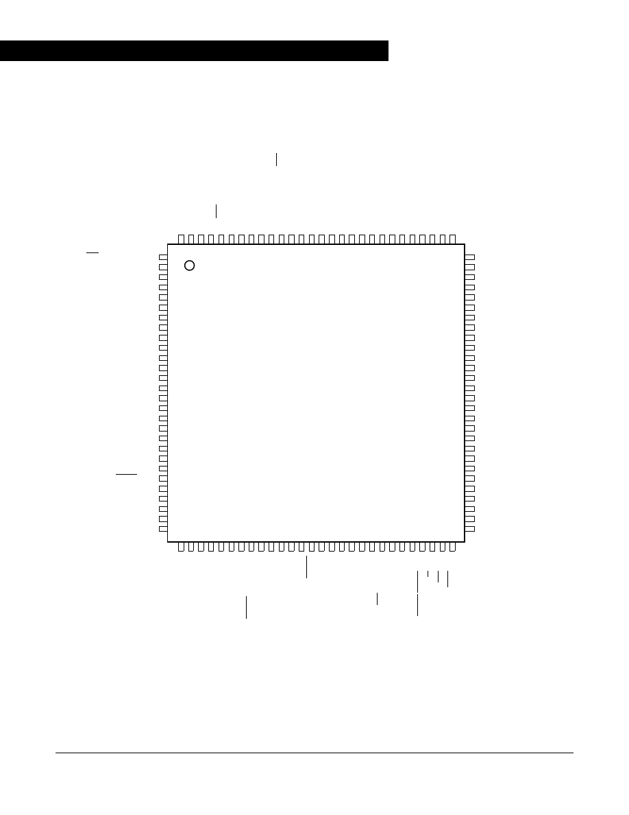
Figure 2. Pin Assignments 112 LQFP for MC9S12DB128
VRH
VDDA
PAD15/AN15/ETRIG1
PAD07/AN07/ETRIG0
PAD14/AN14
PAD06/AN06
PAD13/AN13
PAD05/AN05
PAD12/AN12
PAD04/AN04
PAD11/AN11
PAD03/AN03
PAD10/AN10
PAD02/AN02
PAD09/AN09
PAD01/AN01
PAD08/AN08
PAD00/AN00
VSS2
VDD2
PA7/ADDR15/DATA15
PA6/ADDR14/DATA14
PA5/ADDR13/DATA13
PA4/ADDR12/DATA12
PA3/ADDR11/DATA11
PA2/ADDR10/DATA10
PA1/ADDR9/DATA9
PA0/ADDR8/DATA8
PP4/KWP4/PW
M4
PP5/KPW5/PW
M5
PP6/KWP6/PW
M6
PP7/KWP7/PW
M7
PK7/ECS
/R
OMCTL
VDDX
VSSX
PM0/R
XCAN0/RXB
PM1/T
XCAN0/TXB
PM2/R
X
_BF/RXCAN0
/MISO0
PM3/T
X
_BF/TXCA
N0/S
S0
PM4/B
F_PSYN/RXCAN
0/R
XCAN4/MOSI0
PM5/B
F_PR
O
K/TXCAN
0/T
X
CAN4/SCK0
PJ6/KWJ6/RXCAN4
/SD
A
PJ7/KWJ7/TXCAN4
/SCL
VREGEN
PS7/SS0
PS6/SCK0
PS5/MOSI0
PS4/MISO0
PS3/TXD1
PS2/RXD1
PS1/TXD0
PS0/RXD0
PM6/B
F_PERR/RXCAN
4
PM7/B
F_PSLM/TXC
AN4
VSSA
VRL
SS1/PWM3/KWP3/PP3
SCK1/PWM2/KWP2/PP2
MOSI1/PWM1/KWP1/PP1
MISO1/PWM0/KWP0/PP0
XADDR17/PK3
XADDR16/PK2
XADDR15/PK1
XADDR14/PK0
IOC0/PT0
IOC1/PT1
IOC2/PT2
IOC3/PT3
VDD1
VSS1
IOC4/PT4
IOC5/PT5
IOC6/PT6
IOC7/PT7
XADDR19/PK5
XADDR18/PK4
KWJ1/PJ1
KWJ0/PJ0
MODC/TAGHI/BKGD
ADDR0/DATA0/PB0
ADDR1/DATA1/PB1
ADDR2/DATA2/PB2
ADDR3/DATA3/PB3
ADDR4/DATA4/PB4
ADDR5/D
AT
A
5/PB
5
ADDR6/D
AT
A
6/PB
6
ADDR7/D
AT
A
7/PB
7
KW
H7
/P
H7
KW
H6
/P
H6
KW
H5
/P
H5
KW
H4
/P
H4
XCLKS
/NO
A
CC/PE
7
MODB/
IP
IPE
1/PE
6
MOD
A
/IP
IPE
0/PE
5
ECL
K/PE
4
V
SSR
V
DDR
RESE
T
VDDPL
L
XF
C
VSSPL
L
EXT
A
L
XT
A
L
TES
T
SS
1/K
WH
3/PH
3
SC
K1/K
W
H
2/PH
2
M
O
S
I1
/KW
H1
/P
H1
M
IS
O
1/
KW
H0
/P
H0
LSTRB
/T
A
G
LO
/PE
3
R/W
/PE
2
IRQ
/PE
1
XIRQ
/PE
0
Signals shown in Bold are not available on the 80 Pin Package
MC9S12DB128
112LQFP
11
2
11
1
11
0
10
9
10
8
10
7
10
6
10
5
10
4
10
3
10
2
10
1
10
0
99
98
97
96
95
94
93
92
91
90
89
88
87
86
85
1
2
3
4
5
6
7
8
9
10
11
12
13
14
15
16
17
18
19
20
21
22
23
24
25
26
27
28
29
30
31
32
33
34
35
36
37
38
39
40
41
42
43
44
45
46
47
48
49
50
51
52
53
54
55
56
84
83
82
81
80
79
78
77
76
75
74
73
72
71
70
69
68
67
66
65
64
63
62
61
60
59
58
57
HCS12DBFAMILYPP/D
Pin Out Explanations:
MOTOROLA
HCS12DB Family Product Proposal
7
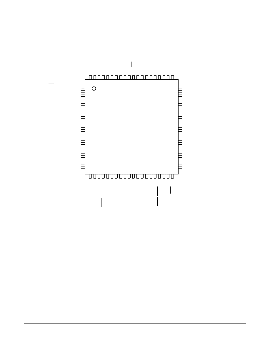
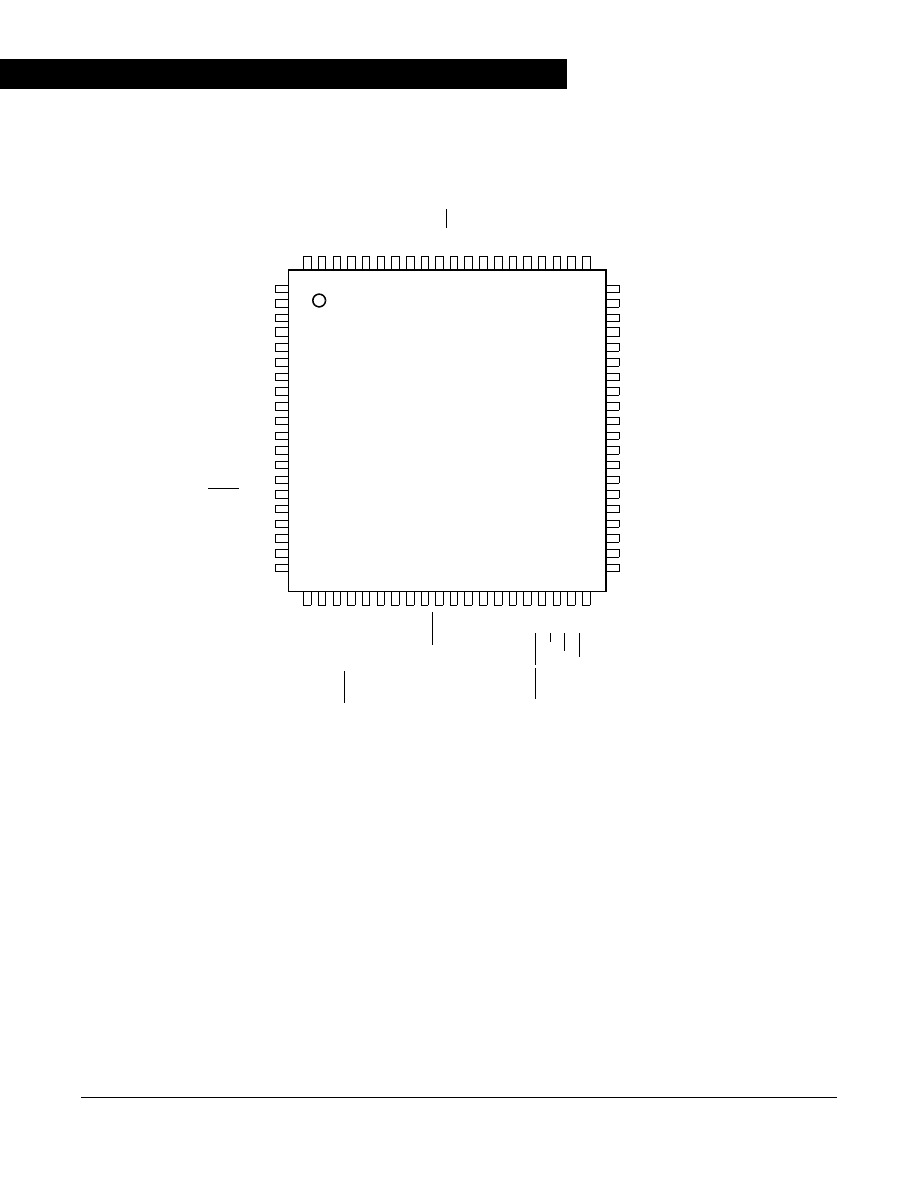
Figure 3.
Pin Assignments MC9S12DB128 in 80 QFP
1
2
3
4
5
6
7
8
9
10
11
12
13
14
15
16
17
18
19
20
80
79
78
77
76
75
74
73
72
71
70
69
68
67
66
65
64
63
62
61
21
22
23
24
25
26
27
28
29
30
31
32
33
34
35
36
37
38
39
40
MC9S12DB128
80 QFP
VRH
VDDA
PAD07/AN07/ETRIG0
PAD06/AN06
PAD05/AN05
PAD04/AN04
PAD03/AN03
PAD02/AN02
PAD01/AN01
PAD00/AN00
VSS2
VDD2
PA7/ADDR15/DATA15
PA6/ADDR14/DATA14
PA5/ADDR13/DATA13
PA4/ADDR12/DATA12
PA3/ADDR11/DATA11
PA2/ADDR10/DATA10
PA1/ADDR9/DATA9
PA0/ADDR8/DATA8
PP4/KWP4/P
W
M4
PP5/KWP5/P
W
M5
PP7/KWP7/P
W
M7
VDDX
VSSX
PM2/R
X
_BF
PM3/T
X
_BF
PM4/B
F_PSYN
PM5/B
F_PR
O
K
VREGEN
PS7/SS0
PS6/SCK0
PS5/MOSI0
PS4/MISO0
PS1/TXD0
PS0/RXD0
PM6/B
F_PERR
BF_PSL
M
VSSA
VRL
SS1/PWM3/KWP3/PP3
SCK1/PWM2/KWP2/PP2
MOSI1/PWM1/KWP1/PP1
MISO1/PWM0/KWP0/PP0
IOC0/PT0
IOC1/PT1
IOC2/PT2
IOC3/PT3
VDD1
VSS1
IOC4/PT4
IOC5/PT5
IOC6/PT6
IOC7/PT7
MODC/TAGHI/BKGD
ADDR0/DATA0/PB0
ADDR1/DATA1/PB1
ADDR2/DATA2/PB2
ADDR3/DATA3/PB3
ADDR4/DATA4/PB4
ADDR5
/D
AT
A5/PB5
ADDR6
/D
AT
A6/PB6
ADDR7
/D
AT
A7/PB7
XC
LKS
/NO
A
CC/PE7
MODB/IPIPE1/PE6
MOD
A/IPIPE0/PE5
ECLK/PE4
VSSR
VDDR
RESET
VD
DPLL
XFC
VS
SPLL
EXT
AL
XT
AL
TEST
LST
R
B
/T
A
G
LO
/PE3
R/W
/PE2
IRQ
/PE1
XIRQ
/PE0
60
59
58
57
56
55
54
53
52
51
50
49
48
47
46
45
44
43
42
41
HCS12DBFAMILYPP/D
8
HCS12DB Family Product Proposal
MOTOROLA
Figure 4.
Pin Assignments MC9S12DB64 in 80 QFP
1
2
3
4
5
6
7
8
9
10
11
12
13
14
15
16
17
18
19
20
80
79
78
77
76
75
74
73
72
71
70
69
68
67
66
65
64
63
62
61
21
22
23
24
25
26
27
28
29
30
31
32
33
34
35
36
37
38
39
40
MC9S12DB64
80 QFP
VRH
VDDA
PAD07/AN07/ETRIG0
PAD06/AN06
PAD05/AN05
PAD04/AN04
PAD03/AN03
PAD02/AN02
PAD01/AN01
PAD00/AN00
VSS2
VDD2
PA7/ADDR15/DATA15
PA6/ADDR14/DATA14
PA5/ADDR13/DATA13
PA4/ADDR12/DATA12
PA3/ADDR11/DATA11
PA2/ADDR10/DATA10
PA1/ADDR9/DATA9
PA0/ADDR8/DATA8
PP4/KWP4/P
W
M4
PP5/KWP5/P
W
M5
PP7/KWP7/P
W
M7
VDDX
VSSX
PM2/R
X
_BF
PM3/T
X
_BF
PM4/B
F_PSYN
PM5/B
F_PR
O
K
VREGEN
PS7/SS0
PS6/SCK0
PS5/MOSI0
PS4/MISO0
PS1/TXD0
PS0/RXD0
PM6/B
F_PERR
BF_PSL
M
VSSA
VRL
PWM3/KWP3/PP3
PWM2/KWP2/PP2
PWM1/KWP1/PP1
PWM0/KWP0/PP0
IOC0/PT0
IOC1/PT1
IOC2/PT2
IOC3/PT3
VDD1
VSS1
IOC4/PT4
IOC5/PT5
IOC6/PT6
IOC7/PT7
MODC/TAGHI/BKGD
ADDR0/DATA0/PB0
ADDR1/DATA1/PB1
ADDR2/DATA2/PB2
ADDR3/DATA3/PB3
ADDR4/DATA4/PB4
ADDR5
/D
AT
A5/PB5
ADDR6
/D
AT
A6/PB6
ADDR7
/D
AT
A7/PB7
XC
LKS
/NO
A
CC/PE7
MODB/IPIPE1/PE6
MOD
A/IPIPE0/PE5
ECLK/PE4
VSSR
VDDR
RESET
VD
DPLL
XFC
VS
SPLL
EXT
AL
XT
AL
TEST
LST
R
B
/T
A
G
LO
/PE3
R/W
/PE2
IRQ
/PE1
XIRQ
/PE0
60
59
58
57
56
55
54
53
52
51
50
49
48
47
46
45
44
43
42
41
HCS12DBFAMILYPP/D
Pin Out Explanations:
MOTOROLA
HCS12DB Family Product Proposal
9
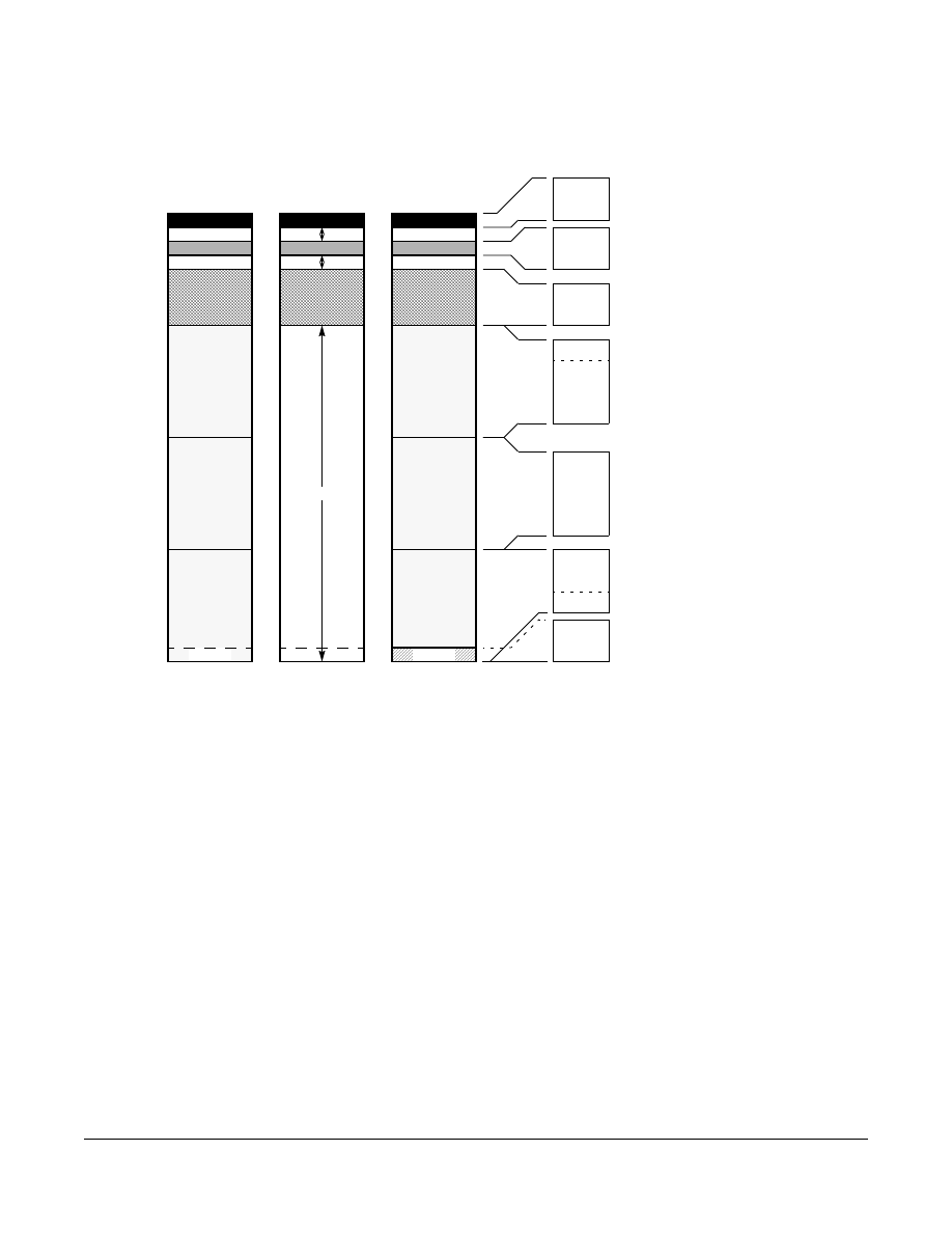
Figure 5. MC9S12DB128 User Configurable Memory Map
$0000
$FFFF
$C000
$8000
$4000
$0400
$0800
$1000
$2000
$FF00
EXT
NORMAL
SINGLE CHIP
EXPANDED
SPECIAL
SINGLE CHIP
VECTORS
VECTORS
VECTORS
$FF00
$FFFF
BDM
(If Active)
$C000
$FFFF
16K Fixed Flash EEPROM
2K, 4K, 8K or 16K Protected Boot Sector
$8000
$BFFF
16K Page Window
Eight * 16K Flash EEPROM Pages
$4000
$7FFF
16K Fixed Flash EEPROM
0.5K, 1K, 2K or 4K Protected Sector
$2000
$3FFF
8K Bytes RAM
Mappable to any 8K Boundary
$0800
$0FFF
2K Bytes EEPROM
Mappable to any 2K Boundary
$0000
$03FF
1K Register Space
Mappable to any 2K Boundary
The address does not show the map after reset, but a useful map. After reset the map is:
$0000 - $03FF: Register Space
$0000 - $1FFF: 8K RAM
$0000 - $07FF: 2K EEPROM (not visible)
HCS12DBFAMILYPP/D
10
HCS12DB Family Product Proposal
MOTOROLA
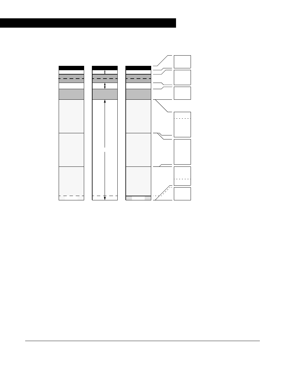
Figure 6.
MC9S12DB64 User Configurable Memory Map
$0000
$FFFF
$C000
$8000
$4000
$0400
$0800
$1000
$3000
$FF00
EXT
NORMAL
SINGLE CHIP
EXPANDED
SPECIAL
SINGLE CHIP
VECTORS
VECTORS
VECTORS
$FF00
$FFFF
BDM
(If Active)
$C000
$FFFF
16K Fixed Flash EEPROM
2K, 4K, 8K or 16K Protected Boot Sector
$8000
$BFFF
16K Page Window
four * 16K Flash EEPROM Pages
$4000
$7FFF
16K Fixed Flash EEPROM
0.5K, 1K, 2K or 4K Protected Sector
$2000
$3FFF
8K Bytes RAM
Mappable to any 4K Boundary
$0800
$0FFF
2K Bytes EEPROM
Mappable to any 2K Boundary
$0000
$03FF
1K Register Space
Mappable to any 2K Boundary
The figure shows a useful map, which is not the map out of reset. After reset the map is:
$0000 - $03FF: Register Space
$0000 - $1FFF: 8K RAM
$0000 - $07FF: 2K EEPROM (not visible)
$0C00

HCS12DBFAMILYPP/D
Pin Out Explanations:
MOTOROLA
HCS12DB Family Product Proposal
11
This page intentionally left blank.

HOW TO REACH US:
USA/EUROPE/LOCATIONS NOT LISTED:
Motorola Literature Distribution
P.O. Box 5405, Denver, Colorado 80217
1-800-521-6274 or 480-768-2130
JAPAN:
Motorola Japan Ltd.
SPS, Technical Information Center
3-20-1, Minami-Azabu
Minato-ku
Tokyo 106-8573, Japan
81-3-3440-3569
ASIA/PACIFIC:
Motorola Semiconductors H.K. Ltd.
Silicon Harbour Centre
2 Dai King Street
Tai Po Industrial Estate
Tai Po, N.T. Hong Kong
852-26668334
HOME PAGE:
http://motorola.com/semiconductors
Information in this document is provided solely to enable system and software
implementers to use Motorola products. There are no express or implied copyright
licenses granted hereunder to design or fabricate any integrated circuits or
integrated circuits based on the information in this document.
Motorola reserves the right to make changes without further notice to any products
herein. Motorola makes no warranty, representation or guarantee regarding the
suitability of its products for any particular purpose, nor does Motorola assume any
liability arising out of the application or use of any product or circuit, and specifically
disclaims any and all liability, including without limitation consequential or incidental
damages. “Typical” parameters which may be provided in Motorola data sheets
and/or specifications can and do vary in different applications and actual
performance may vary over time. All operating parameters, including “Typicals”
must be validated for each customer application by customer’s technical experts.
Motorola does not convey any license under its patent rights nor the rights of
others. Motorola products are not designed, intended, or authorized for use as
components in systems intended for surgical implant into the body, or other
applications intended to support or sustain life, or for any other application in which
the failure of the Motorola product could create a situation where personal injury or
death may occur. Should Buyer purchase or use Motorola products for any such
unintended or unauthorized application, Buyer shall indemnify and hold Motorola
and its officers, employees, subsidiaries, affiliates, and distributors harmless
against all claims, costs, damages, and expenses, and reasonable attorney fees
arising out of, directly or indirectly, any claim of personal injury or death associated
with such unintended or unauthorized use, even if such claim alleges that Motorola
was negligent regarding the design or manufacture of the part.
Motorola and the Stylized M Logo are registered in the U.S. Patent and Trademark
Office. digital dna is a trademark of Motorola, Inc. All other product or service
names are the property of their respective owners. Motorola, Inc. is an Equal
Opportunity/Affirmative Action Employer.
© Motorola, Inc. 2003
HCS12DBFAMILYPP/D
Rev. 0.7
Document Outline
Wyszukiwarka
Podobne podstrony:
MC9S12DF HCS12DF Family Product Brief
MC9S12C HCS12C Family Product Brief
A9 product brief
A7 ipcam product brief
A7 dvcam product brief
A9 product brief
Luminus SST90 Product Brief Eng
TAVOR Assault Rifle family katalog reklamowy producenta
Product presentation XC100FC
~$Production Of Speech Part 2
Product presentation easyControl
Wykład nr 5 podstawy decyzji producenta
Overview of Exploration and Production
family spaghetti
Family 2
Ek w 5, Producent, 25mar11 [t Nieznany
CM 52 ProductDefinition oct2011
produkcja-pytania, PWR, ZiIP Zarządzanie i Inżynieria Produckji, ZPiU Chlebus
więcej podobnych podstron