PCB Impedance Control:
Formulas and Resources
Douglas Brooks, President
UltraCAD Design, Inc.
This article appeared in Printed Circuit Design Magazine, March, 1998
1998 Miller Freeman, Inc
1998 UltraCAD Design, Inc.
Many of the formulas we use for PCB impedance
calculations are readily available, but not all of them. In
fact, while we are often quick to say that PCBs begin to
look like transmission lines when rise times are fast enough,
and perhaps toss out a few formulas for our readers, we
miss at least three factors when we do so.
Not complete: It's not enough to say that Zo equals
some complex formula. We may also want to know other
parameters, such as propagation time, intrinsic capacitance,
intrinsic inductance, and the effects of device loading and
terminations. I know of no single source where all of these
formulas are made available.
Too complex: Even if the formulas are available, they
can be so complex that even a person with a considerable
background in mathematics can't use them without an intol-
erable probability of arithmetic error.
Not right form: It is fine, for example, to say that Zo is
some complex function of width, thickness, and height
above the plane. But what if what you really want to know
is what width to use to hit a given Zo? Or what height is
required? Most of our readers are not prepared to tackle
this type of formula manipulation.
This article will do two things: (1) bring together all
the relevant formulas into one place, along with source
references, and (2) show you where there are several, free
resources available for dealing with them.
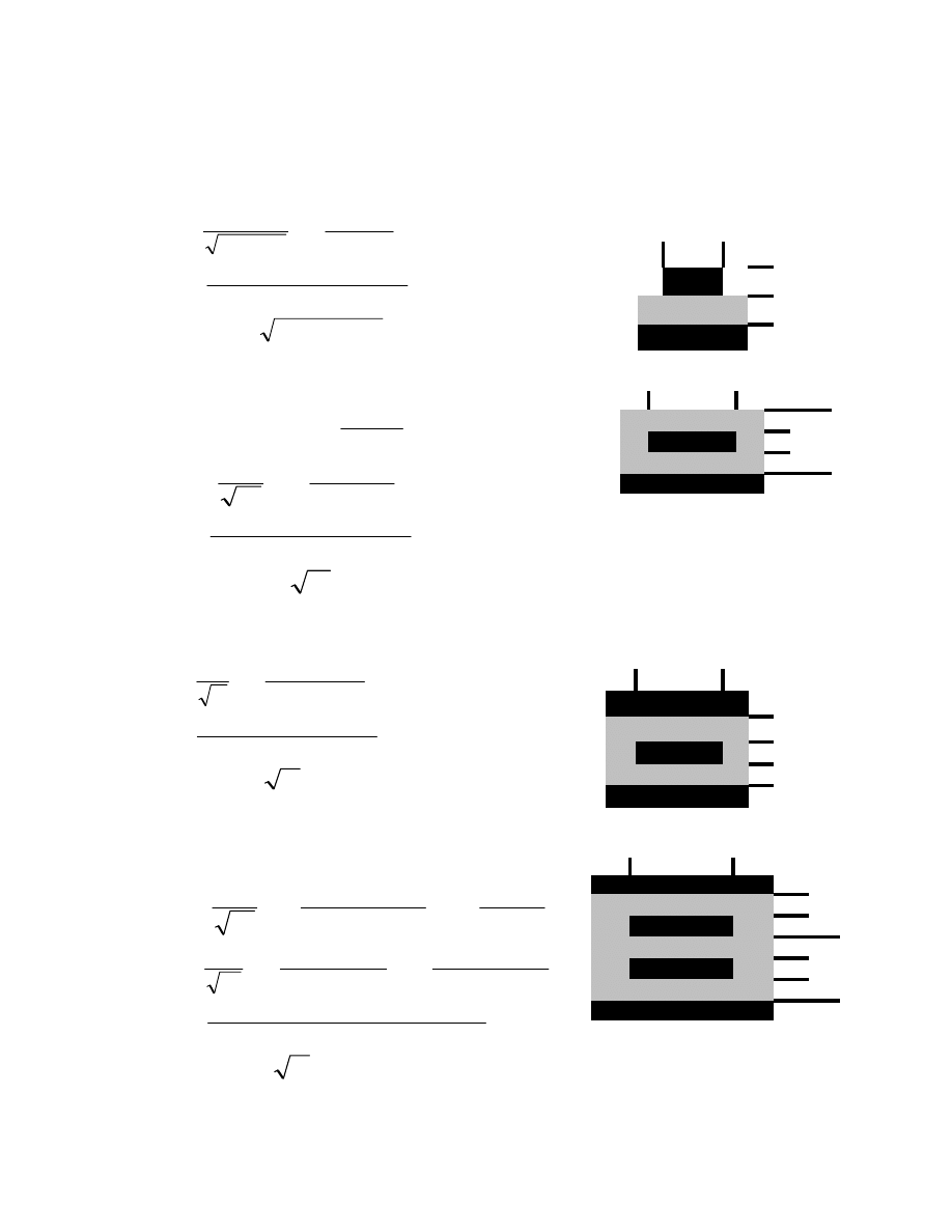
The formulas
Figure 1 provides the basic formulas for Zo (in Ohms),
Co (in pf/in) and Tpd (ns/in) for the most common PCB
trace configurations. While many sources have some of
these formulas, I only know of one source
(footnote 1)
that
contains all of them. One note, however, about embedded
microstrip. The adjustment for the relative dielectric coeffi-
cient is reasonable if the material above the trace is more
than 4 mils thick and is of the same dielectric coefficient as
the material below the trace. If the thickness is less than
that, or if the dielectric coefficient is lower than the material
below the trace, the actual result will be between those
calculated for microstrip and for embedded microstrip.
Note also that the embedded microstrip configuration,
for infinite embedding, is the same as asymmetric stripline
with one plane infinitely far away. Yet the formulas, while
close, do not give identical results in this cases. This illus-
trates the problem with all these formulas. They are approxi-
mations and are based on simplifying assumptions. But they
are only guides; none will give exact results. If exact results
are really important, get your board fabricator on board early
in the design process and rely on their expertise.
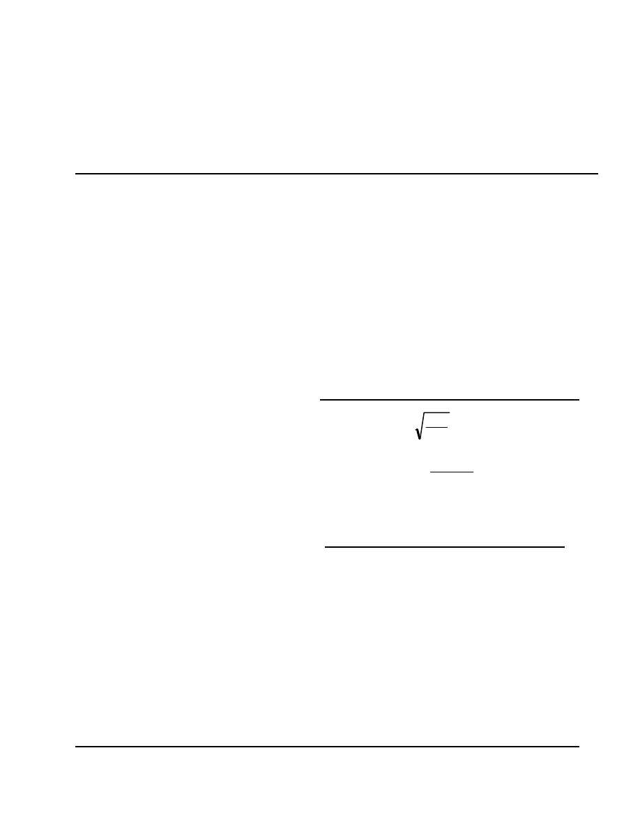
Almost all references point out that for a transmission
line, Zo is the square root of Lo/Co. (Figure 2a) Therefore,
the intrinsic inductance, Lo, can be calculated as shown in
Figure 2b. At least one source provides the formula shown in
Figure 2c for calculating the inductance of a flat trace over a
plane.
(footnote 2)
The results of these two formulas for
microstrip can differ by as much as 10%, which illustrates
again that all these formulas are approximations based on
simplifying assumptions, and different approaches can
sometimes lead to different results.
(a)
Zo
Lo
Co
=
Ohms
(b)
Lo
Co
Zo
=
*
2
pH/in
(c)
L
Ln
Pi
H
W
=
F
HG
I
KJ
5
2
*
*
*
nH/in
Figure 2
Formulas for trace impedance
Devices placed along a trace add capacitance. This
capacitance "loading" has an effect on both Zo and on
Tpd. The correction factor is the square root of (1 +
Cd/Co*l) where Cd is the sum of the capacitive loads
and l is the length of the trace (Figure 3a). The correc-
tion factors for Zo and Tpd are shown in Figure 3b and
3c.
These adjustments are correct for parallel termina-
tions and they are found in most references. Motorola
has a complicated derivation that shows an additional
effect from series termination. (
Footnote 3
). The theory
is complex, but fundamentally involves the fact that the
(
)
(
)
+
+
=
T
W
T
H
Ln
Z
r
8
.
2
9
.
1
60
0
ε
+
+
=
T
W
H
Ln
Z
r
8
.
98
.
5
41
.
1
87
0
ε
Stripline
Microstrip
)]
8
/(.
98
.
5
[
)
41
.
1
(
67
.
0
T
W
H
Ln
C
r
+
+
=
ε
)]
8
/(.
81
.
3
[
41
.
1
0
T
W
H
Ln
C
r
+
=
ε
+
+
−
+
+
=
)
(
4
1
)
8
(.
)
2
(
9
.
1
80
0
T
C
H
H
T
W
T
H
Ln
Z
r
ε
Dual or Asymmetric Stripline
)]
335
.
268
/(.
)
(
2
[
82
.
2
0
T
W
T
H
Ln
C
r
+
−
=
ε
W
H
T
H
W
H
T
C
T
H1
H
W
T
H
Embedded Microstrip
.67
+
.475
1.017
=
t
r
pd
ε
r
pd
1.017
=
t
ε
r
pd
1.017
=
t
ε
−
+
+
=
)
1
(
4
1
)
8
(.
)
2
(
9
.
1
80
0
H
H
T
W
T
H
Ln
Z
r
ε
−
−
=
H
H
r
r
1
55
.
1
exp
1
'
ε
ε
W
|
T
H1
H
|
+
=
T
W
H
Ln
Z
r
8
.
98
.
5
'
60
0
ε
)]
8
/(.
98
.
5
[
)
'
(
41
.
1
0
T
W
H
Ln
C
r
+
=
ε
'
.08475
=
t
r
pd
ε
First, let:
Figure 1
Formulas for impedance calculations. Units for Zo, Co, and Tpd are Ohms, Pf/in, and ns/in, respectively.
Transmission Line Formulas

capacitive loads are charged through the series load,
somewhat slowing down the rise time, and therefore the
propagation time, of the trace. The adjusted correction
factor for series termination is shown in Figure 3d. Note
that in all these cases the adjustment factor collapses to 1.0
if Cd = 0.
Finally, the voltage reflection coefficient,
ρ
, of a
transmission line is given by
ρ
= (R
L
- Zo)/(R
L
+ Zo)
One characteristic of a transmission line is that if it is
terminated in a resistive load equal to its characteristic
impedance (Zo), a signal traveling down the trace will be
completely absorbed by the load and not reflect back. If
the trace is left open at the far end (R
L
is infinite), the
signal reflects back with the same polarity and magnitude.
But if the trace is shorted at the far end (R
L
= 0 and
therefore
ρ
= -1), the signal reflects back with the same
magnitude but the opposite polarity.
The Resources
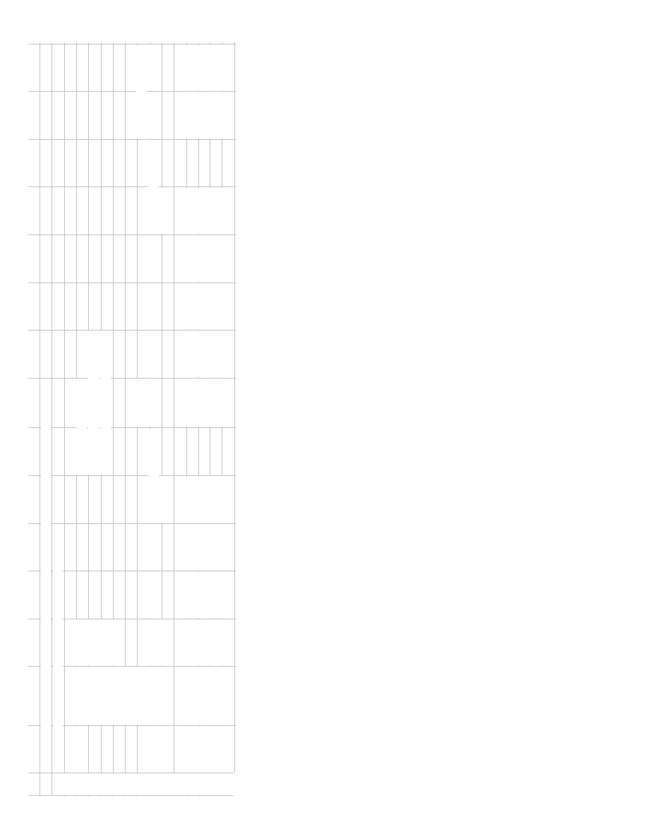
It is really not too difficult to build your own spread-
sheet to make these calculations. An example is shown in
Figure 4a and the formulas for row 14 are shown in
Figure 4b.
(footnote 4)
These formulas can simply be
copied to additional rows to show the effects of a wide
range of relative dielectric coefficients. Building a spread-
sheet has the added benefit that you can build graphs to
(
)
l
Co
Cd
*
1
+
(
)
l
Co
Cd
t
t
pd
pd
*
1
'
+
=
1
1
*
1
*
2
+
−
+
l
Co
Cd
l
*
Co
Cd
+
1
Zo
=
Zo'
(a) Correction Factor
(b) Impact on Zo
(c) Impact on Tpd
(d) Correction Factor for
Series Termination
Figure 3
Impact of Capacitive Loading
illustrate various relationships, and solve for any variable
(perhaps, though, through an interative process).
Barry Olney has an interactive web site where you can
enter various parameters, and it will display the impedance of
the various trace layers. The web site can be found at
www.icd.com.au/board/board.html.
Polar Instruments, Ltd. has a freeware Windows calcula-
tor that allows you to calculate several trace parameters given
the others. You can obtain this calculator at www.polar.co.uk
and follow the link to the calculator. It is not readily apparent
that you need to enter the data in mils or mm or significant
round off error may result.
UltraCAD Design, Inc. has a freeware Windows calcula-
tor that has all the formulas contained in this article, and that
can solve for virtually any parameter given the others. It also
has a help file that discusses the formulas and their sources.
You can obtain it at www.ultracad.com and follow the links to
"calculators."
Note: The article, as published, contained illustrations of
these last three resources. The illustrations have been omitted
here because the pictures added almost 900k to the .pdf file!
Summary
Articles and seminars have shown you the significance,
importance, and impact of transmission lines on PCBs. The
formulas and their sources are summarized here, but can
admittedly be difficult to use. There are, however, several
freeware resources available to you on the web and elsewhere
that can simplify this task. The only thing left is for you to
take advantage of these resources.
Footnotes
1. IPC-D-317, April, 1990, “Design Guidelines for Electronic
Packaging Utilizing High-Speed Techniques”, pp. 17-25.
2. Ott, Henry, “Noise Reduction Techniques in Electronics,”
Wiley Interscience, 1988, p. 281
3. “MECL System Design Handbook,” Rev. 1, Motorola
Semiconductor Products, Inc. 1988, p. 157
4. These formulas are correct for Quattro Pro and for Lotus
1-2-3. They might need some very minor adjustments for
Excel spreadsheets.
B14 2
C14 87*@LN(5.98*$D$5/(0.8*$D$7+$D$6))/(B14+1.41)^0.5
D14 0.67*(B14+1.41)/@LN(5.98*$D$5/(0.8*$D$7+$D$6))
E14 1.017*(0.475*B14+0.67)^0.5
F14 12/E14
G14 (C14^2)*D14/1000
I14 60*@LN((4*(2*$D$5+$D$6))/(0.67*3.14159*(0.8*$D$7+$D$6)))/((B14)^0.5)
J14 1.41*B14/@LN(3.81*$D$5/(0.8*$D$7+$D$6))
K14 1.017*(B14)^0.5
L14 12/K14
M14 (I14^2)*J14/1000
O14 80*(1-$D$5/(4*($D$5+$D$8+$D$6))))*@LN(1.9*(2*$D$5+$D$6)/(0.8*$D$7+$D$6))/(B14)^0.5
P14 2.82*B14/@LN(2*($D$5-$D$6)/(0.268*$D$7+0.335*$D$6))
Figure 4b
Formulas used in spreadsheet example
P
O
N
M
L
K
J
I
H
G
F
E
D
C
B
1
This program is set up to calculate various impedances and capacitances associated
2
with strip lines, microstrips, etc. Enter data in inches.
3
4
Zo is in ohms
0.009
h =
let:
5
Co is capacitance (pf)/inch
0.0008
t =
6
Tp is propagation delay in ns/ft
0.01
w =
7
0.0076
c =
8
9
Dual Stripline
Stripline
Microstrip
10
Co
Zo
Inductance
Tp in/ns
Tp ns/ft
Co
Zo
Inductance
Tp in/ns
Tp ns/ft
Co
Zo
dialectric
11
(nH/in)
(nH/in)
(pf/in)
(Ohms)
coeff
12
13
3.286
69.002
7.327
8.343
1.438
2.073
59.446
9.183
9.270
1.294
1.262
85.317
2.0
14
3.451
67.339
7.327
8.142
1.474
2.177
58.013
9.183
9.137
1.313
1.299
84.093
2.1
15
3.615
65.791
7.327
7.955
1.508
2.281
56.679
9.183
9.010
1.332
1.336
82.920
2.2
16
3.779
64.345
7.327
7.780
1.542
2.384
55.433
9.183
8.888
1.350
1.373
81.795
2.3
17
Figure 4a Spreadsheet can be used for impedance calculations
Wyszukiwarka
Podobne podstrony:
Money Management Controlling Risk And Capturing Profits
SSP 406 DCC Adaptive Chassis Control Design and Function
99 Best Blogging Tools and Resources
MASTERS OF PERSUASION Power, Politics, Money Laundering, Nazi’s, Mind Control, Murder and Medjugore
Hultgren; Baptism in the New Testament Origins, Formulas, and Metaphors
12 Werntges controling KNX from Linux and USB
Control of Redundant Robot Manipulators R V Patel and F Shadpey
Control and Instrumentation Engineer?scription
Marijuana is one of the most discussed and controversial topics around the world
P4 explain how an individual?n exercise command and control
Mantak Chia 4th Formula Greatest Kan and Li (47 pages)
Lynge Odeon A Design Tool For Auditorium Acoustics, Noise Control And Loudspeaker Systems
Human resources in science and technology
Power Converters And Control Renewable Energy Systems
Causes and control of filamentous growth in aerobic granular sludge sequencing batch reactors
What is command and control
Mantak Chia 3rd Formula Greater Kan and Li (53 pages)
więcej podobnych podstron