TL/F/6527
5475/DM5475/DM7475
Quad
Latches
June 1989
5475/DM5475/DM7475
Quad Latches
General Description
These latches are ideally suited for use as temporary stor-
age for binary information between processing units and in-
put/output or indicator units. Information present at a data
(D) input is transferred to the Q input when the enable (G) is
high, and the Q output will follow the data input as long as
the enable remains high. When the enable goes low, the
information (that was present at the data input at the time
the transition occurred) is retained at the Q output until the
enable is permitted to go high.
These latches feature complementary Q and Q outputs
from a 4-bit latch and are available in 16-pin packages.
Features
Y
Alternate Military/Aerospace device (5475) is available.
Contact a National Semiconductor Sales Office/Distrib-
utor for specifications.
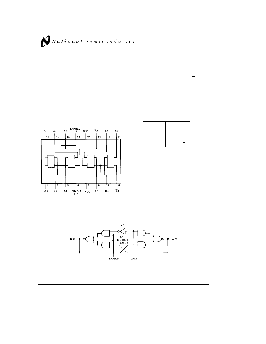
Connection Diagram
Dual-In-Line Package
TL/F/6527 – 1
Order Number 5475DMQB, 5475FMQB, DM5475J,
DM5475W or DM7475N
See NS Package Number J16A, N16E or W16A
Function Table
(Each Latch)
Inputs
Outputs
D
G
Q
Q
L
H
L
H
H
H
H
L
X
L
Q
0
Q
0
H
e
High Level, L
e
Low Level, X
e
Don’t
Care, Q
0
e
The Level of Q Before the High-
to-Low Transition of G
Logic Diagram
(Each Latch)
TL/F/6527 – 2
C1995 National Semiconductor Corporation
RRD-B30M105/Printed in U. S. A.
Absolute Maximum Ratings
(Note)
If Military/Aerospace specified devices are required,
please contact the National Semiconductor Sales
Office/Distributors for availability and specifications.
Supply Voltage
7V
Input Voltage
5.5V
Operating Free Air Temperature Range
DM54 and 54
b
55
§
C to
a
125
§
C
DM74
0
§
C to
a
70
§
C
Storage Temperature Range
b
65
§
C to
a
150
§
C
Note:
The ‘‘Absolute Maximum Ratings’’ are those values
beyond which the safety of the device cannot be guaran-
teed. The device should not be operated at these limits. The
parametric values defined in the ‘‘Electrical Characteristics’’
table are not guaranteed at the absolute maximum ratings.
The ‘‘Recommended Operating Conditions’’ table will define
the conditions for actual device operation.
Recommended Operating Conditions
Symbol
Parameter
DM5475
DM7475
Units
Min
Nom
Max
Min
Nom
Max
V
CC
Supply Voltage
4.5
5
5.5
4.75
5
5.25
V
V
IH
High Level Input Voltage
2
2
V
V
IL
Low Level Input Voltage
0.8
0.8
V
I
OH
High Level Output Current
b
0.4
b
0.4
mA
I
OL
Low Level Output Current
16
16
mA
t
W
Enable Pulse Width (Note 4)
20
20
ns
t
SU
Setup Time (Note 4)
20
20
ns
t
H
Hold Time (Note 4)
5
5
ns
T
A
Free Air Operating Temperature
b
55
125
0
70
§
C
Electrical Characteristics
over recommended operating free air temperature range (unless otherwise noted)
Symbol
Parameter
Conditions
Min
Typ
Max
Units
(Note 1)
V
I
Input Clamp Voltage
V
CC
e
Min, I
I
e b
12 mA
b
1.5
V
V
OH
High Level Output
V
CC
e
Min, I
OH
e
Max
2.4
3.4
V
Voltage
V
IL
e
Max, V
IH
e
Min
V
OL
Low Level Output
V
CC
e
Min, I
OL
e
Max
0.2
0.4
V
Voltage
V
IH
e
Min, V
IL
e
Max
I
I
Input Current
@
Max
V
CC
e
Max, V
I
e
5.5V
1
mA
Input Voltage
I
IH
High Level Input Current
V
CC
e
Max, V
I
e
2.4V
80
m
A
I
IL
Low Level Input Current
V
CC
e
Max, V
I
e
0.4V
b
3.2
mA
I
OS
Short Circuit
V
CC
e
Max
DM54
b
20
b
55
mA
Output Current
(Note 2)
DM74
b
18
b
55
I
CC
Supply Current
V
CC
e
Max
DM54
32
46
mA
(Note 3)
DM74
32
50
Note 1:
All typicals are at V
CC
e
5V, T
A
e
25
§
C.
Note 2:
Not more than one output should be shorted at a time.
Note 3:
I
CC
is measured with all inputs grounded and all outputs open.
Note 4:
T
A
e
25
§
C and V
CC
e
5V.
2
Switching Characteristics
at V
CC
e
5V and T
A
e
25
§
C (See Section 1 for Test Waveforms and Output Load)
From (Input)
R
L
e
400X
Symbol
Parameter
To (Output)
C
L
e
15 pF
Units
Min
Max
t
PHL
Propagation Delay Time
D to Q
25
ns
High to Low Level Output
t
PLH
Propagation Delay Time
D to Q
30
ns
Low to High Level Output
t
PHL
Propagation Delay Time
D to Q
15
ns
High to Low Level Output
t
PLH
Propagation Delay Time
D to Q
40
ns
Low to High Level Output
t
PHL
Propagation Delay Time
G to Q
15
ns
High to Low Level Output
t
PLH
Propagation Delay Time
G to Q
30
ns
Low to High Level Output
t
PHL
Propagation Delay Time
G to Q
15
ns
High to Low Level Output
t
PLH
Propagation Delay Time
G to Q
30
ns
Low to High Level Output
3

4
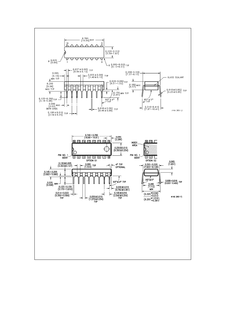
Physical Dimensions
inches (millimeters)
16-Lead Ceramic Dual-In-Line Package (J)
Order Number 5475DMQB or DM5475J
NS Package Number J16A
16-Lead Molded Dual-In-Line Package (N)
Order Number DM7475N
NS Package Number N16E
5
5475/DM5475/DM7475
Quad
Latches
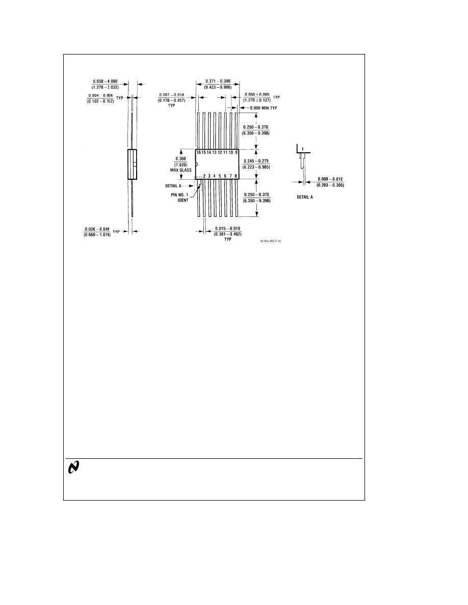
Physical Dimensions
inches (millimeters) (Continued)
16-Lead Ceramic Flat Package (W)
Order Number 5475FMQB or DM5475W
NS Package Number W16A
LIFE SUPPORT POLICY
NATIONAL’S PRODUCTS ARE NOT AUTHORIZED FOR USE AS CRITICAL COMPONENTS IN LIFE SUPPORT
DEVICES OR SYSTEMS WITHOUT THE EXPRESS WRITTEN APPROVAL OF THE PRESIDENT OF NATIONAL
SEMICONDUCTOR CORPORATION. As used herein:
1. Life support devices or systems are devices or
2. A critical component is any component of a life
systems which, (a) are intended for surgical implant
support device or system whose failure to perform can
into the body, or (b) support or sustain life, and whose
be reasonably expected to cause the failure of the life
failure to perform, when properly used in accordance
support device or system, or to affect its safety or
with instructions for use provided in the labeling, can
effectiveness.
be reasonably expected to result in a significant injury
to the user.
National Semiconductor
National Semiconductor
National Semiconductor
National Semiconductor
Corporation
Europe
Hong Kong Ltd.
Japan Ltd.
1111 West Bardin Road
Fax: (a49) 0-180-530 85 86
13th Floor, Straight Block,
Tel: 81-043-299-2309
Arlington, TX 76017
Email: cnjwge
@
tevm2.nsc.com
Ocean Centre, 5 Canton Rd.
Fax: 81-043-299-2408
Tel: 1(800) 272-9959
Deutsch Tel: (a49) 0-180-530 85 85
Tsimshatsui, Kowloon
Fax: 1(800) 737-7018
English
Tel: (a49) 0-180-532 78 32
Hong Kong
Fran
3ais Tel: (a49) 0-180-532 93 58
Tel: (852) 2737-1600
Italiano
Tel: (a49) 0-180-534 16 80
Fax: (852) 2736-9960
National does not assume any responsibility for use of any circuitry described, no circuit patent licenses are implied and National reserves the right at any time without notice to change said circuitry and specifications.

This datasheet has been download from:
Datasheets for electronics components.
Wyszukiwarka
Podobne podstrony:
7475
Układy synchroniczne i asynchroniczne( przerzutnik typu D i zatrzask RS), Zespół Szkół Elektrycznych
Zatrzask
F1 59 Zatrzaski 1
7475
F1 61 Zatrzaski 3
Drzwi zatrzasniete przed nosem
Zatrzaśnięcie kluczyka w?gażniku
7475
F1 60 Zatrzaski 2
praca-magisterska-wa-c-7475, Dokumenty(2)
honda civic jazz polaczenia zatrzaskowe
7475
więcej podobnych podstron