MP1593
3A, 28V, 385KHz
Step-Down
Converter
MP1593 Rev. 1.7
www.MonolithicPower.com
1
10/20/2005
MPS Proprietary Information. Unauthorized Photocopy and Duplication Prohibited.
© 2005 MPS. All Rights Reserved.
The Future of Analog IC Technology
TM
TM
DESCRIPTION
The MP1593 is a step-down regulator with an
internal Power MOSFET. It achieves 3A
continuous output current over a wide input
supply range with excellent load and line
regulation.
Current mode operation provides fast transient
response and eases loop stabilization.
Fault condition protection includes cycle-by-cycle
current limiting and thermal shutdown. Adjustable
soft-start reduces the stress on the input source
at turn-on. In shutdown mode the regulator draws
2
0µA
of supply current.
The MP1593 requires a minimum number of
readily available external components to
complete a 3A step down DC to DC converter
solution.
EVALUATION BOARD REFERENCE
Board Number
Dimensions
EV1593DN-00A
2.1”X x 1.3”Y x 0.4”Z
FEATURES
• 3A Output Current
• Programmable Soft-Start
• 100mΩ Internal Power MOSFET Switch
• Stable with Low ESR Output Ceramic
Capacitors
• Up to 95% Efficiency
• 20µA Shutdown Mode
• Fixed 385KHz Frequency
• Thermal
Shutdown
• Cycle-by-Cycle Over Current Protection
• Wide 4.75V to 28V Operating Input Range
• Output Adjustable from 1.22V
• Under Voltage Lockout
• Available in 8-Pin SOIC Package
APPLICATIONS
• Distributed
Power
Systems
• Battery
Chargers
• Pre-Regulator for Linear Regulators
• Flat
Panel
TVs
• Set-Top
Boxes
• Cigarette Lighter Powered Devices
• DVD/PVR
Devices
“MPS” and “The Future of Analog IC Technology” are Trademarks of Monolithic
Power Systems, Inc.
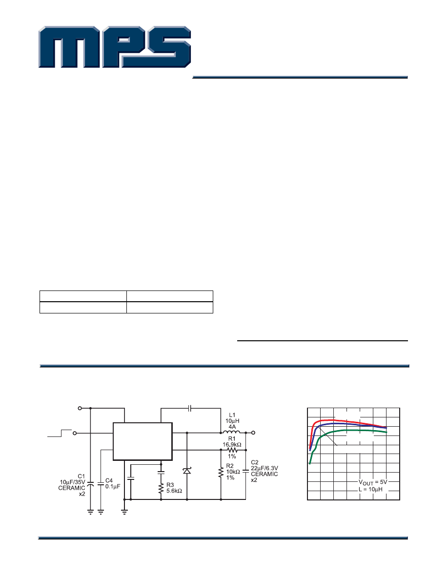
TYPICAL APPLICATION
INPUT
4.75V to 28V
OUTPUT
3.3V
3A
C3
8.2nF
D1
B340A
C5
10nF
MP1593
BS
IN
FB
SW
SS
GND
COMP
EN
C6
(optional)
MP1593_TAC01
1
3
5
6
4
8
7
2
OFF ON
EFFICIENCY
(%)
100
95
90
85
80
75
70
65
60
55
50
LOAD CURRENT (mA)
MP1593_TAC _EC01
Efficiency vs
Load Current
0
500 1000 1500 2000 2500 3000 3500
V
IN
= 9V
V
IN
= 12V
V
IN
= 24V
MP1593 – 3A, 28V, 385KHz STEP-DOWN CONVERTER
MP1593 Rev. 1.7
www.MonolithicPower.com
2
10/20/2005
MPS Proprietary Information. Unauthorized Photocopy and Duplication Prohibited.
© 2005 MPS. All Rights Reserved.
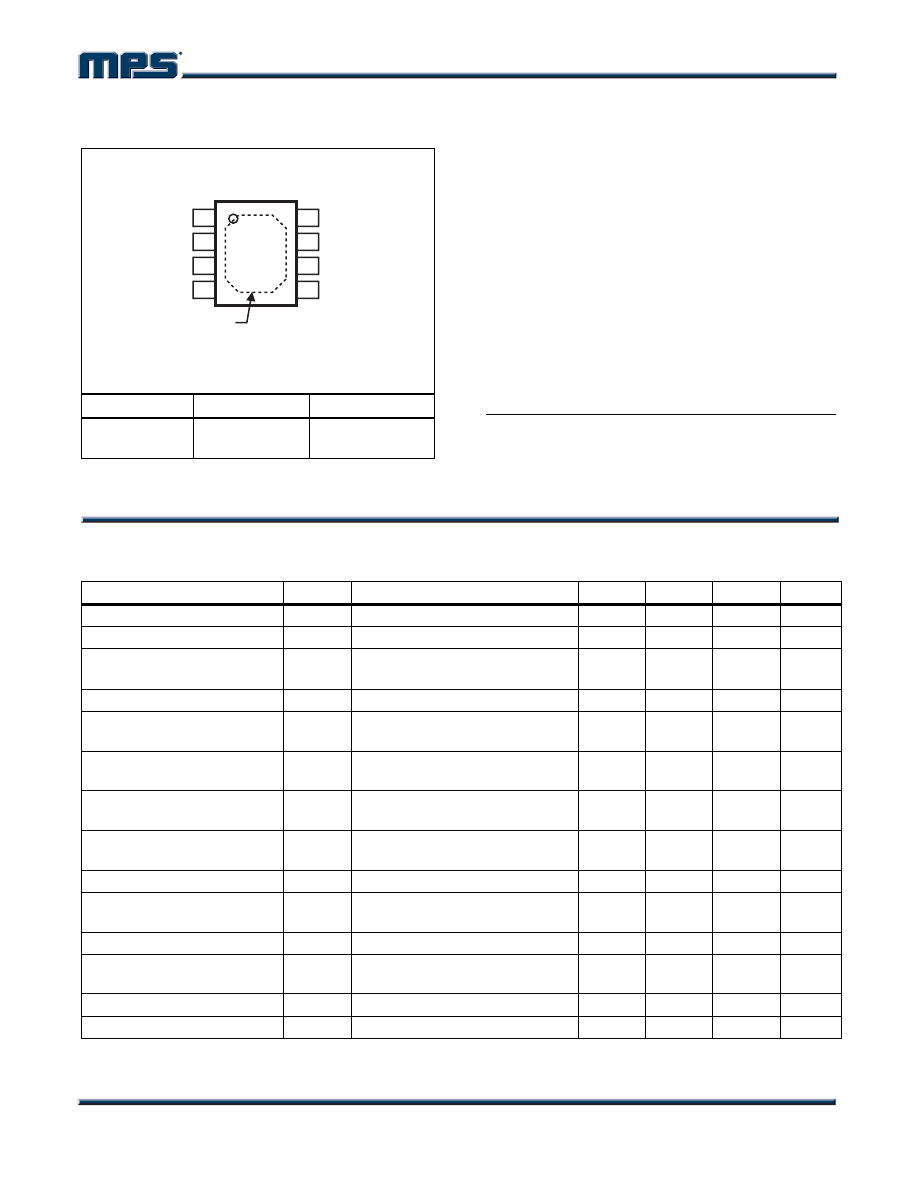
PACKAGE REFERENCE
Part Number*
Package
Temperature
MP1593DN
SOIC8N
(Exposed Pad) –40°C to +85°C
*
For Tape & Reel, add suffix –Z (eg. MP1593DN–Z)
For Lead Free, add suffix –LF (eg. MP1593DN–LF–Z)
ABSOLUTE MAXIMUM RATINGS
(1)
Supply Voltage V
IN
......................... –0.3V to 30V
Switch Voltage V
SW
.............. –0.5V to V
IN
+ 0.3V
Boost Voltage V
BS
..........V
SW
– 0.3V to V
SW
+ 6V
All Other Pins................................. –0.3V to +6V
Junction Temperature...............................150
°C
Lead Temperature ....................................260
°C
Storage Temperature ...............–65°C to 150
°C
Recommended Operating Conditions
(2)
Input Voltage V
IN
............................ 4.75V to 28V
Ambient Operating Temp............. –40
°C to +85°C
Thermal Resistance
(3)
θ
JA
θ
JC
SOIC8N (w/Exposed Pad)...... 50 ...... 10...
°C/W
Notes:
1) Exceeding these ratings may damage the device.
2) The device is not guaranteed to function outside of its
operating conditions.
3) Measured on approximately 1” square of 1 oz copper.
ELECTRICAL CHARACTERISTICS
V
IN
= 12V, T
A
= +25
°C, unless otherwise noted.
Parameter Symbol
Condition
Min
Typ
Max
Units
Shutdown Supply Current
V
EN
= 0V
20
30
µA
Supply Current
V
EN
= 2.6V, V
FB
= 1.4V
1.0
1.2
mA
Feedback Voltage
V
FB
4.75V
≤ V
IN
≤ 28V
V
COMP
< 2V
1.194 1.222 1.250 V
Error Amplifier Voltage Gain
A
EA
400 V/V
Error Amplifier
Transconductance
G
EA
∆I
COMP
=
±10µA
500 800 1120
µA/V
High Side Switch On
Resistance
R
DS(ON)1
100
140
mΩ
Low Side Switch On
Resistance
R
DS(ON)2
10
Ω
High Side Switch Leakage
Current
V
EN
= 0V, V
SW
= 0V
0
10
µA
Current Limit
3.3
4.7
6.5
A
Current Sense to COMP
Transconductance
G
CS
6.2
A/V
Oscillation Frequency
f
OSC1
335
385
435 KHz
Short Circuit Oscillation
Frequency
f
OSC2
V
FB
= 0V
25
45
60
KHz
Maximum Duty Cycle
D
MAX
V
FB
= 1.0V
90
%
Minimum Duty Cycle
D
MIN
V
FB
= 1.5V
0
%
BS
IN
SW
GND
SS
EN
COMP
FB
1
2
3
4
8
7
6
5
TOP VIEW
MP1593_PD01_SOIC8N
EXPOSED PAD
ON BACKSIDE
CONNECT TO PIN 4
MP1593 – 3A, 28V, 385KHz STEP-DOWN CONVERTER
MP1593 Rev. 1.7
www.MonolithicPower.com
3
10/20/2005
MPS Proprietary Information. Unauthorized Photocopy and Duplication Prohibited.
© 2005 MPS. All Rights Reserved.
ELECTRICAL CHARACTERISTICS
(continued)
V
IN
= 12V, T
A
= +25
°C, unless otherwise noted.
Parameter Symbol
Condition
Min
Typ
Max
Units
EN Threshold Voltage
0.9
1.2
1.5
V
Enable Pull Up Current
V
EN
= 0V
1.0
1.7
2.5
µA
Under Voltage Lockout
Threshold
V
IN
Rising
2.3
2.6
2.9
V
Under Voltage Lockout
Threshold Hysteresis
210 mV
Soft Start Period
C
SS
= 0.1µF
10
ms
Thermal Shutdown
160
°C
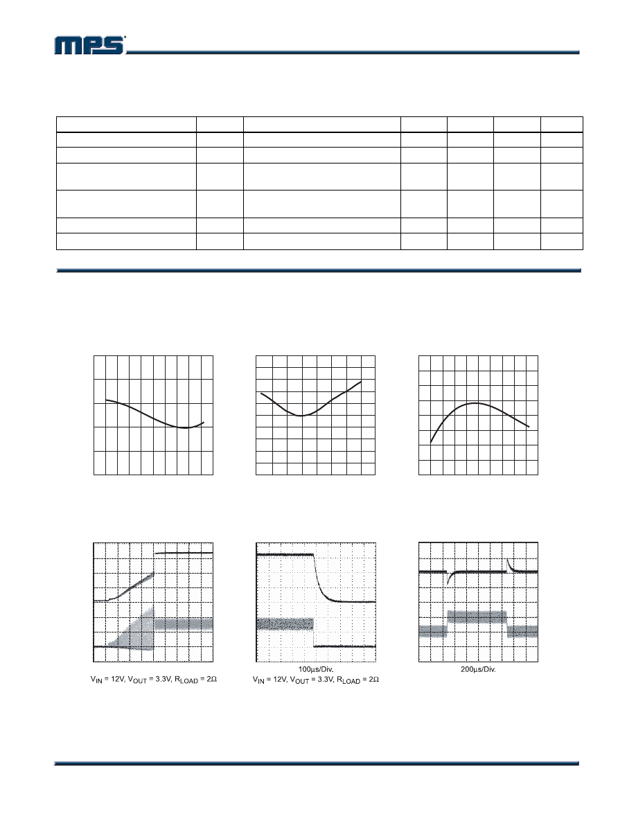
TYPICAL PERFORMANCE CHARACTERISTICS
Refer to Typical Application Schematic on Page 1
420
410
400
390
380
370
360
350
340
OSCILLA
TION FREQUENCY
(KHz)
TEMPERATURE (
°C)
MP1593-TPC03
Oscillation Frequency vs
Temperature
5.0
4.9
4.8
4.7
4.6
4.5
4.4
4.3
4.2
4.1
4.0
PEAK CURRENT
LIMIT
(A)
TEMPERATURE (
°C)
MP1593-TPC02
Peak Current Limit vs
Temperature
1.245
1.235
1.225
1.215
1.205
1.195
FEEDBACK VOL
TAGE (V)
-60 -40 -20 0 20 40 60 80 100 120 140
TEMPERATURE (
°C)
MP1593-TPC01
Feedback Voltage vs
Temperature
-50 -25 -0
25
50
75 100 125 150
-60 -40 -20 0 20 40 60 80 100 120 140
MP1593-TPC04
Soft-Start
Waveforms
V
OUT
1V/Div.
I
L
1A/Div.
4ms/Div.
V
OUT
1V/Div.
I
L
1A/Div.
MP1593-TPC05
Turn Off
Waveforms
V
OUT
100mV/Div.
I
L
1A/Div.
V
IN
= 12V, V
OUT
= 3.3V, 1A - 2A STEP
MP1593-TPC-06
Load Transient
Waveforms
MP1593 – 3A, 28V, 385KHz STEP-DOWN CONVERTER
MP1593 Rev. 1.7
www.MonolithicPower.com
4
10/20/2005
MPS Proprietary Information. Unauthorized Photocopy and Duplication Prohibited.
© 2005 MPS. All Rights Reserved.
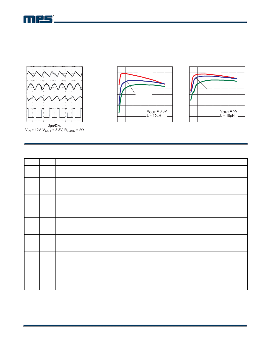
TYPICAL PERFORMANCE CHARACTERISTICS
(continued)
Refer to Typical Application Schematic on Page 1
EFFICIENCY
(%)
100
95
90
85
80
75
70
65
60
55
50
LOAD CURRENT (mA)
MP1593_TPC09
Efficiency vs
Load Current
0
500 1000 1500 2000 2500 3000 3500
V
IN
= 9V
V
IN
= 12V
V
IN
= 24V
100
95
90
85
80
75
70
65
60
55
50
EFFICIENCY
(%)
0
500 1000 1500 2000 2500 3000 3500
LOAD CURRENT (mA)
MP1593_TPC08
Efficiency vs
Load Current
V
IN
= 5V
V
IN
= 24V
V
IN
= 12V
I
L
1A/Div.
V
OUT
10mV/Div.
V
SW
10V/Div.
V
IN
100mV/Div.
MP1593-TPC07
Switching
Waveforms
PIN FUNCTIONS
Pin # Name Description
1 BS
High-Side Gate Drive Boost Input. BS supplies the drive for the high-side N-Channel MOSFET
switch. Connect a 10nF or greater capacitor from SW to BS to power the high side switch.
2 IN
Power Input. IN supplies the power to the IC, as well as the step-down converter switches. Drive
IN with a 4.75V to 28V power source. Bypass IN to GND with a suitably large capacitor to
eliminate noise on the input to the IC. See Input Capacitor section.
3 SW
Power Switching Output. SW is the switching node that supplies power to the output. Connect
the output LC filter from SW to the output load. Note that a capacitor is required from SW to BS
to power the high-side switch.
4
GND Ground. (Note: Connect the exposed pad on backside to Pin 4).
5 FB
Feedback Input. FB senses the output voltage to regulate that voltage. Drive FB with a resistive
voltage divider from the output voltage. The feedback threshold is 1.222V. See Setting the
Output Voltage section.
6 COMP
Compensation Node. COMP is used to compensate the regulation control loop. Connect a series
RC network from COMP to GND to compensate the regulation control loop. In some cases, an
additional capacitor from COMP to GND is required. See Compensation section.
7 EN
Enable Input. EN is a digital input that turns the regulator on or off. Drive EN high to turn on the
regulator, drive EN low to turn it off. An Under Voltage Lockout (UVLO) function can be
implemented by the addition of a resistor divider from V
IN
to GND. For complete low current
shutdown its needs to be less than 0.7V. For automatic startup, leave EN unconnected.
8 SS
Soft-Start Control Input. SS controls the soft-start period. Connect a capacitor from SS to GND
to set the soft-start period. A 0.1µF capacitor sets the soft-start period to 10ms. To disable the
soft-start feature, leave SS unconnected.
MP1593 – 3A, 28V, 385KHz STEP-DOWN CONVERTER
MP1593 Rev. 1.7
www.MonolithicPower.com
5
10/20/2005
MPS Proprietary Information. Unauthorized Photocopy and Duplication Prohibited.
© 2005 MPS. All Rights Reserved.
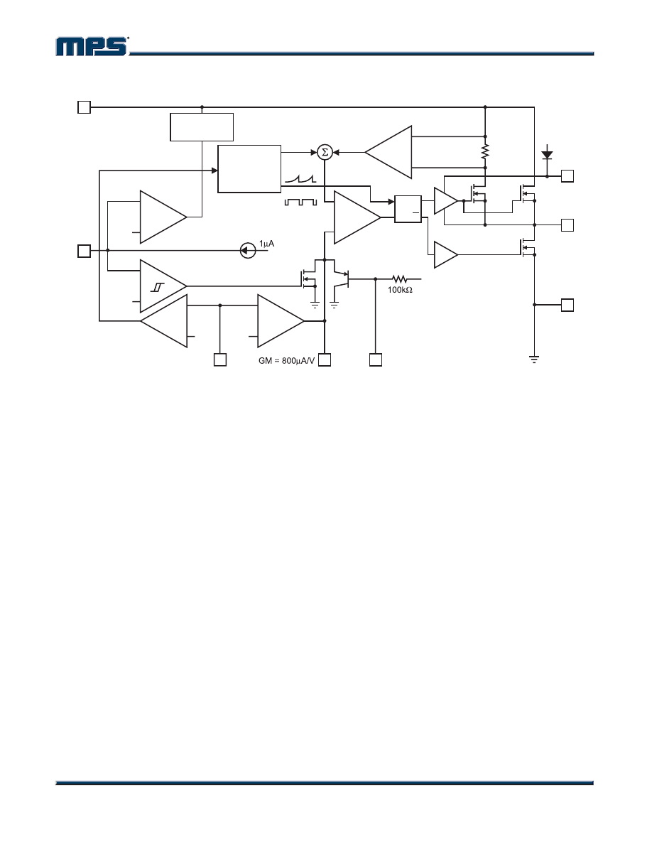
OPERATION
MP1593_BD01
LOCKOUT
COMPARATOR
ERROR
AMPLIFIER
FREQUENCY
FOLDBACK
COMPARATOR
INTERNAL
REGULATORS
1.8V
SLOPE
COMP
CLK
CURRENT
COMPARATOR
CURRENT
SENSE
AMPLIFIER
SHUTDOWN
COMPARATOR
SS
8
COMP
6
IN 2
EN 7
GND
4
OSCILLATOR
40/385KHz
S
R
Q
SW
3
BS
M1
M2
1
5V
+
Q
0.7V
+
+
2.3V/
2.6V
+
1.22V
0.7V
+
+
FB
5
--
--
--
--
--
--
Figure 1—Functional Block Diagram
The MP1593 is a current-mode step-down
regulator. It regulates input voltages from 4.75V to
28V down to an output voltage as low as 1.22V,
and is able to supply up to 3A of load current.
The MP1593 uses current-mode control to
regulate the output voltage. The output voltage
is measured at FB through a resistive voltage
divider and amplified through the internal error
amplifier. The output current of the
transconductance error amplifier is presented at
COMP where a network compensates the
regulation control system. The voltage at COMP
is compared to the switch current measured
internally to control the output voltage.
The converter uses an internal N-Channel
MOSFET switch to step-down the input voltage
to the regulated output voltage. Since the
MOSFET requires a gate voltage greater than
the input voltage, a boost capacitor connected
between SW and BS drives the gate. The
capacitor is internally charged while SW is low.
An internal 10Ω switch from SW to GND is used
to insure that SW is pulled to GND when SW is
low to fully charge the BS
.
capacitor.
MP1593 – 3A, 28V, 385KHz STEP-DOWN CONVERTER
MP1593 Rev. 1.7
www.MonolithicPower.com
6
10/20/2005
MPS Proprietary Information. Unauthorized Photocopy and Duplication Prohibited.
© 2005 MPS. All Rights Reserved.
APPLICATION INFORMATION
COMPONENT SELECTION
Setting the Output Voltage
The output voltage is set using a resistive
voltage divider from the output voltage to FB
pin. The voltage divider divides the output
voltage down to the feedback voltage by the
ratio:
2
R
1
R
2
R
V
V
OUT
FB
+
=
Where V
FB
is the feedback voltage and V
OUT
is
the output voltage.
Thus the output voltage is:
2
R
2
R
1
R
22
.
1
V
OUT
+
×
=
A typical value for R2 can be as high as 100kΩ,
but a typical value is 10kΩ. Using that value, R1
is determined by:
)
k
)(
22
.
1
V
(
18
.
8
1
R
OUT
Ω
−
×
=
For example, for a 3.3V output voltage, R2 is
10kΩ, and R1 is 17kΩ.
Inductor
The inductor is required to supply constant
current to the output load while being driven by
the switched input voltage. A larger value
inductor will result in less ripple current that will
result in lower output ripple voltage. However,
the larger value inductor will have a larger
physical size, higher series resistance, and/or
lower saturation current. A good rule for
determining the inductance to use is to allow
the peak-to-peak ripple current in the inductor
to be approximately 30% of the maximum
switch current limit. Also, make sure that the
peak inductor current is below the maximum
switch current limit. The inductance value can
be calculated by:
⎟⎟
⎠
⎞
⎜⎜
⎝
⎛
−
×
×
=
IN
OUT
L
S
OUT
V
V
1
∆I
f
V
L
Where V
IN
is the input voltage, f
S
is the 385KHz
switching frequency, and ∆I
L
is the peak-to-
peak inductor ripple current.
Choose an inductor that will not saturate under
the maximum inductor peak current. The peak
inductor current can be calculated by:
⎟⎟
⎠
⎞
⎜⎜
⎝
⎛
−
×
×
×
+
=
IN
OUT
S
OUT
LOAD
LP
V
V
1
L
f
2
V
I
I
Where I
LOAD
is the load current.
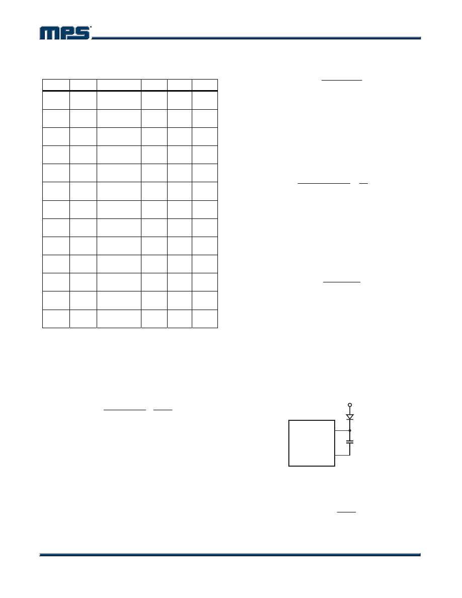
Table 1 lists a number of suitable inductors
from various manufacturers. The choice of
which style inductor to use mainly depends on
the price vs. size requirements and any EMI
requirement.
Table 1—Inductor Selection Guide
Package
Dimensions
(mm)
Vendor/
Model
Core
Type
Core
Material
W L H
Sumida
CR75
Open Ferrite 7.0 7.8 5.5
CDH74 Open Ferrite 7.3 8.0 5.2
CDRH5D28 Shielded
Ferrite 5.5 5.7 5.5
CDRH5D28 Shielded
Ferrite 5.5 5.7 5.5
CDRH6D28 Shielded
Ferrite 6.7 6.7 3.0
CDRH104R Shielded
Ferrite 10.1 10.0 3.0
Toko
D53LC
Type A
Shielded
Ferrite 5.0 5.0 3.0
D75C Shielded
Ferrite 7.6 7.6 5.1
D104C Shielded
Ferrite 10.0 10.0 4.3
D10FL
Open Ferrite 9.7 1.5 4.0
Coilcraft
DO3308 Open Ferrite 9.4
13.0 3.0
DO3316 Open Ferrite 9.4
13.0 5.1
MP1593 – 3A, 28V, 385KHz STEP-DOWN CONVERTER
MP1593 Rev. 1.7
www.MonolithicPower.com
7
10/20/2005
MPS Proprietary Information. Unauthorized Photocopy and Duplication Prohibited.
© 2005 MPS. All Rights Reserved.
Output Rectifier Diode
The output rectifier diode supplies the current to
the inductor when the high-side switch is off. To
reduce losses due to the diode forward voltage
and recovery times, use a Schottky diode.
Choose a diode whose maximum reverse
voltage rating is greater than the maximum
input voltage, and whose current rating is
greater than the maximum load current. Table 2
lists example Schottky diodes and
manufacturers.
Table 2—Diode Selection Guide
Diode
Voltage/Current
Rating
Manufacture
SK33
30V, 3A
Diodes Inc.
SK34
40V, 3A
Diodes Inc.
B330
30V, 3A
Diodes Inc.
B340
40V, 3A
Diodes Inc.
MBRS330
30V, 3A
On Semiconductor
MBRS340
40V, 3A
On Semiconductor
Input Capacitor
The input current to the step-down converter is
discontinuous, therefore a capacitor is required
to supply the AC current to the step-down
converter while maintaining the DC input
voltage. Use low ESR capacitors for the best
performance. Ceramic capacitors are preferred,
but tantalum or low-ESR electrolytic capacitors
may also suffice.
Since the input capacitor absorbs the input
switching current it requires an adequate ripple
current rating. The RMS current in the input
capacitor can be estimated by:
⎟
⎟
⎠
⎞
⎜
⎜
⎝
⎛
×
−
×
=
IN
OUT
IN
OUT
LOAD
CIN
V
V
1
V
V
I
I
The worst-case condition occurs at V
IN
= 2V
OUT
,
where:
2
I
I
LOAD
CIN
=
For simplification, choose the input capacitor
whose RMS current rating greater than half of
the maximum load current.
The input capacitor can be electrolytic, tantalum
or ceramic. When using electrolytic or tantalum
capacitors, a small, high quality ceramic
capacitor, i.e. 0.1µF, should be placed as close
to the IC as possible. When using ceramic
capacitors, make sure that they have enough
capacitance to provide sufficient charge to
prevent excessive voltage ripple at input. The
input voltage ripple caused by capacitance can
be estimated by:
⎟⎟
⎠
⎞
⎜⎜
⎝
⎛
−
×
×
×
=
∆
IN
OUT
IN
OUT
IN
S
LOAD
IN
V
V
1
V
V
C
f
I
V
Where C
IN
is the input capacitance value.
Output Capacitor
The output capacitor is required to maintain the
DC output voltage. Ceramic, tantalum, or low
ESR electrolytic capacitors are recommended.
Low ESR capacitors are preferred to keep the
output voltage ripple low. The output voltage
ripple can be estimated by:
⎟⎟
⎠
⎞
⎜⎜
⎝
⎛
×
×
+
×
⎟⎟
⎠
⎞
⎜⎜
⎝
⎛
−
×
×
=
∆
O
S
ESR
IN
OUT
S
OUT
OUT
C
f
8
1
R
V
V
1
L
f
V
V
Where L is the inductor value, C
O
is the output
capacitance value, and R
ESR
is the equivalent
series resistance (ESR) value of the output
capacitor.
In the case of ceramic capacitors, the
impedance at the switching frequency is
dominated by the capacitance. The output
voltage ripple is mainly caused by the
capacitance. For simplification, the output
voltage ripple can be estimated by:
⎟⎟
⎠
⎞
⎜⎜
⎝
⎛
−
×
×
×
×
=
IN
OUT
O
2
S
OUT
OUT
V
V
1
C
L
f
8
V
∆V
In the case of tantalum or electrolytic
capacitors, the ESR dominates the impedance
at the switching frequency. For simplification,
the output ripple can be approximated to:
ESR
IN
OUT
S
OUT
OUT
R
V
V
1
L
f
V
∆V
×
⎟⎟
⎠
⎞
⎜⎜
⎝
⎛
−
×
×
=
The characteristics of the output capacitor also
affect the stability of the regulation system. The
MP1593 can be optimized for a wide range of
capacitance and ESR values.
MP1593 – 3A, 28V, 385KHz STEP-DOWN CONVERTER
MP1593 Rev. 1.7
www.MonolithicPower.com
8
10/20/2005
MPS Proprietary Information. Unauthorized Photocopy and Duplication Prohibited.
© 2005 MPS. All Rights Reserved.
Compensation Components
MP1593 employs current mode control for easy
compensation and fast transient response. The
system stability and transient response are
controlled through the COMP pin. COMP pin is
the output of the internal transconductance
error amplifier. A series capacitor-resistor
combination sets a pole-zero combination to
control the characteristics of the control system.
The DC gain of the voltage feedback loop is
given by:
OUT
FB
VEA
CS
LOAD
VDC
V
V
A
G
R
A
×
×
×
=
Where A
VEA
is the error amplifier voltage gain,
400V/V, G
CS
is the current sense
transconductance, 5.9A/V, and R
LOAD
is the load
resistor value.
The system has two poles of importance. One
is due to the compensation capacitor (C3) and
the output resistor of error amplifier, and the
other is due to the output capacitor and the load
resistor. These poles are located at:
VEA
EA
1
P
A
3
C
2
G
f
×
×
π
=
LOAD
O
2
P
R
C
2
1
f
×
×
π
=
Where G
EA
is the error amplifier
transconductance, 800µA/V.
The system has one zero of importance, due to
the compensation capacitor (C3) and the
compensation resistor (R3). This zero is located
at:
3
R
3
C
2
1
f
1
Z
×
×
π
=
The system may have another zero of
importance, if the output capacitor has a large
capacitance and/or a high ESR value. The zero,
due to the ESR and capacitance of the output
capacitor, is located at:
ESR
O
ESR
R
C
2
1
f
×
×
π
=
In this case (as shown in Figure 3), a third pole
set by the compensation capacitor (C6) and the
compensation resistor (R3) is used to
compensate the effect of the ESR zero on the
loop gain. This pole is located at:
3
R
6
C
2
1
f
3
P
×
×
π
=
The goal of compensation design is to shape
the converter transfer function to get a desired
loop gain. The system crossover frequency
where the feedback loop has the unity gain is
important.
Lower crossover frequencies result in slower
line and load transient responses, while higher
crossover frequencies could cause system
unstable. A good rule of thumb is to set the
crossover frequency to approximately one-tenth
of the switching frequency. Switching frequency
for the MP1593 is 385KHz, so the desired
crossover frequency is around 38KHz.
Table 3 lists the typical values of compensation
components for some standard output voltages
with various output capacitors and inductors.
The values of the compensation components
have been optimized for fast transient
responses and good stability at given
conditions.
MP1593 – 3A, 28V, 385KHz STEP-DOWN CONVERTER
MP1593 Rev. 1.7
www.MonolithicPower.com
9
10/20/2005
MPS Proprietary Information. Unauthorized Photocopy and Duplication Prohibited.
© 2005 MPS. All Rights Reserved.
Table 3—Compensation Values for Typical
Output Voltage/Capacitor Combinations
V
OUT
L
C
O
R3
C3
C6
1.8V 4.7µH
100µF
Ceramic
5.6kΩ 3.3nF
None
2.5V 4.7-
6.8µH
47µF
Ceramic
3.9kΩ 5.6nF
None
3.3V 6.8-
10µH
22µFx2
Ceramic
5.6kΩ 8.2nF
None
5V 10-
15µH
22µFx2
Ceramic
7.5kΩ 10nF None
12V 15-
22µH
22µFx2
Ceramic
10kΩ 3.3nF
None
1.8 4.7µH 100µF
SP-CAP
5.6kΩ 3.3nF 100pF
2.5V 4.7-
6.8µH
47µF
SP-CAP
4.7kΩ 5.6nF
None
3.3V 6.8-
10µH
47µF
SP-CAP
6.8kΩ 10nF None
5V 10-
15µH
47µF
SP CAP
10kΩ 10nF None
2.5V 4.7-
6.8µH
560µF Al.
30mΩ ESR
10kΩ 5.6nF
1.5nF
3.3V 6.8-
10µH
560µF Al
30mΩ ESR
10kΩ 8.2nF
1.5nF
5V 10-
15µH
470µF Al.
30mΩ ESR
15kΩ 5.6nF
1nF
12V 15-
22µH
220µF Al.
30mΩ ESR
15kΩ 4.7nF 390pF
To optimize the compensation components for
conditions not listed in Table 3, the following
procedure can be used.
1. Choose the compensation resistor (R3) to set
the desired crossover frequency. Determine the
R3 value by the following equation:
FB
OUT
CS
EA
C
O
V
V
G
G
f
C
2
3
R
×
×
×
×
π
=
Where f
C
is the desired crossover frequency
(which typically has a value no higher than
38KHz).
2. Choose the compensation capacitor (C3) to
achieve the desired phase margin. For
applications with typical inductor values, setting
the compensation zero, f
Z1
, below one forth of
the crossover frequency provides sufficient
phase margin.
Determine the C3 value by the following equation:
C
f
3
R
2
4
3
C
×
×
π
>
Where, R3 is the compensation resistor value and
f
C
is the desired crossover frequency, 38KHz.
3. Determine if the second compensation
capacitor (C6) is required. It is required if the ESR
zero of the output capacitor is located at less than
half of the 385KHz switching frequency, or the
following relationship is valid:
2
f
R
C
2
1
S
ESR
O
<
×
×
π
Where, C
O
is the output capacitance value, R
ESR
is the ESR value of the output capacitor, and f
S
is
the 385KHz switching frequency. If this is the
case, then add the second compensation
capacitor (C6) to set the pole f
P3
at the location of
the ESR zero. Determine the C6 value by the
equation:
3
R
R
C
6
C
ESR
O
×
=
Where, C
O
is the output capacitance value, R
ESR
is the ESR value of the output capacitor, and R3
is the compensation resistor.
External Bootstrap Diode
It is recommended that an external bootstrap
diode be added when the system has a 5V fixed
input or the power supply generates a 5V output.
This helps improve the efficiency of the regulator.
The bootstrap diode can be a low cost one such
as IN4148 or BAT54.
MP1593
SW
BS
10nF
5V
MP1593_F02
Figure 2—External Bootstrap Diode
This diode is also recommended for high duty
cycle operation (when
IN
OUT
V
V
>65%) and high
output voltage (V
OUT
>12V) applications.
MP1593 – 3A, 28V, 385KHz STEP-DOWN CONVERTER
MP1593 Rev. 1.7
www.MonolithicPower.com
10
10/20/2005
MPS Proprietary Information. Unauthorized Photocopy and Duplication Prohibited.
© 2005 MPS. All Rights Reserved.
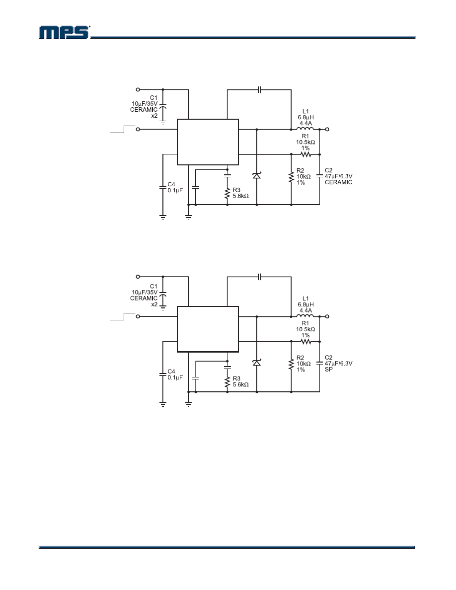
TYPICAL APPLICATION CIRCUITS
INPUT
4.75V to 28V
OUTPUT
2.5V
3A
C3
3.3nF
C6
(optional)
D1
B340A
C5
10nF
MP1593
BS
IN
FB
SW
SS
GND
COMP
EN
MP1593_F03
1
3
5
6
4
8
7
2
OFF ON
Figure 3—MP1593 with AVX 47µF, 6.3V Ceramic Output Capacitor
INPUT
4.75V to 28V
OUTPUT
2.5V
3A
C3
3.3nF
C6
(optional)
D1
B340A
C5
10nF
MP1593
BS
IN
FB
SW
SS
GND
COMP
EN
1
3
5
6
4
8
7
2
MP1593_F04
OFF ON
Figure 4—MP1593 with Panasonic 47µF, 6.3V Special Polymer Output Capacitor
MP1593 – 3A, 28V, 385KHz STEP-DOWN CONVERTER
NOTICE:
The information in this document is subject to change without notice. Please contact MPS for current specifications.
Users should warrant and guarantee that third party Intellectual Property rights are not infringed upon when integrating MPS
products into any application. MPS will not assume any legal responsibility for any said applications.
MP1593 Rev. 1.7
www.MonolithicPower.com
11
10/20/2005
MPS Proprietary Information. Unauthorized Photocopy and Duplication Prohibited.
© 2005 MPS. All Rights Reserved.
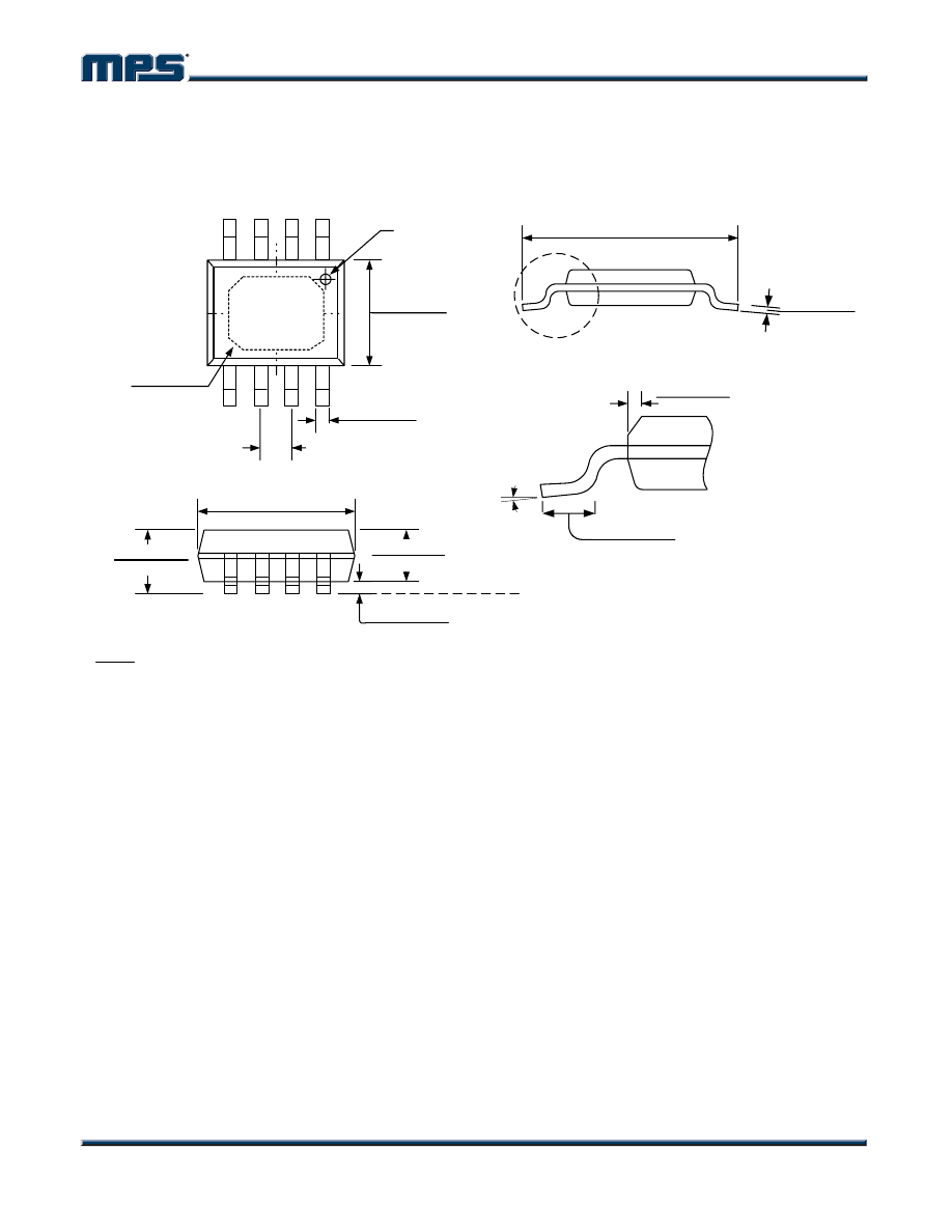
PACKAGE INFORMATION
SOIC8N (EXPOSED PAD)
NOTE:
1) Control dimension is in inches. Dimension in bracket is millimeters.
2) Exposed Pad; 2.55+/- 0.25mm x 3.38 +/- 0.44mm.
Recommended Solder Board Area: 2.80mm x 3.82mm = 10.7mm
2
(16.6mil
2
)
0.016(0.410)
0.050(1.270)
0
o
-8
o
DETAIL "A"
0.011(0.280)
0.020(0.508)
x 45
o
SEE DETAIL "A"
0.0075(0.191)
0.0098(0.249)
0.229(5.820)
0.244(6.200)
SEATING PLANE
0.001(0.030)
0.004(0.101)
0.189(4.800)
0.197(5.004)
0.053(1.350)
0.068(1.730)
0.049(1.250)
0.060(1.524)
0.150(3.810)
0.157(4.000)
PIN 1 IDENT.
0.050(1.270)BSC
0.013(0.330)
0.020(0.508)
NOTE 2
Wyszukiwarka
Podobne podstrony:
MP1593 r1 8
strefy r1
R1 11
01kdpp r1 1
MP2305 r1 3
fema361 chap 5 r1
nierownosci R1
MP2307 r1 1
Ciagi liczbowe R1
MP2106 r1 3
MP1527 r1 8
2 letnie R1 godziny wbinp bid 2 Nieznany (2)
BROWN, R1,3
Marketing egzamin, ZiIP, ZiIP, R1, SII, marketing
Additional Affidavit R1
PIG-R1 2100, Rozdzial I.
więcej podobnych podstron