
Rev.1.00, Sep.22.2003, page 1 of 11
M66515FP
Laser Diode Driver/Controller
REJ03F0084-0100Z
Rev.1.0
Sep.22.2003
Description
The M66515 is a laser diode driver/controller that performs drive and controls the laser power control of a type of
semiconductor laser diode the anode of which is connected, with the cathode of a photodiode for monitoring, to a stem
in which the semiconductor laser diode anode and monitoring photo diode cathode are connected to the stem.
This IC has a sink-type laser driving current output pin, and can drive a laser diode with a bias current of up to a
maximum 30 mA and with switched currents of up to 120 mA, switched at rates of up to 40 Mbps.
The IC incorporates a sample hold circuit, so that a self-APC (Automatic Power Control) system, which does not
require external laser power control, can be realized.
Features
•
Internal sample-and-hold circuit for self-APC configuration
•
High-speed switching (40 Mbps)
•
High driving currents (150 mA max)
•
Settable bias current (30 mA max)
•
Single 5 V power supply
Applications
•
Equipment employing semiconductor laser diodes
Function Overview
The M66515 is a laser diode driver/controller which drives and controls the laser power of a semiconductor laser diode
(LD) the anode of which is connected, with the cathode of a photodiode (PD) for monitoring, to a stem (among
Mitsubishi lasers, N type models).
LD driving and laser power control are executed by connecting an external capacitance to the C
H
pin and applying a
reference voltage to the V
r
pin.
The PD current occurring when a LD emits light flows through a resistance connected across 1RM and 2RM, resulting
in a potential difference (V
M
). This V
M
is compared with the voltage applied to the V
r
pin, and when V
M
<V
r
, a constant
current source from the C
H
pin flows to charge the external capacitor. When V
M
>V
r
, a constant current sink from the
C
H
pin causes the charge on the external capacitor to be discharged.
This operation is performed when the
S/H input is "L" (sample); when the S /H input is in the "H" state, the C
H
pin is in
the high-impedance state (hold), regardless of V
M
, V
r
and the
DATA input state.
The LD driving current consists of a switched current I
SW
, which is controlled by the
DATA input, and I
B
, a LD bias
current which is independent of the
DATA input state.
M66515FP
Rev.1.00, Sep.22.2003, page 2 of 11
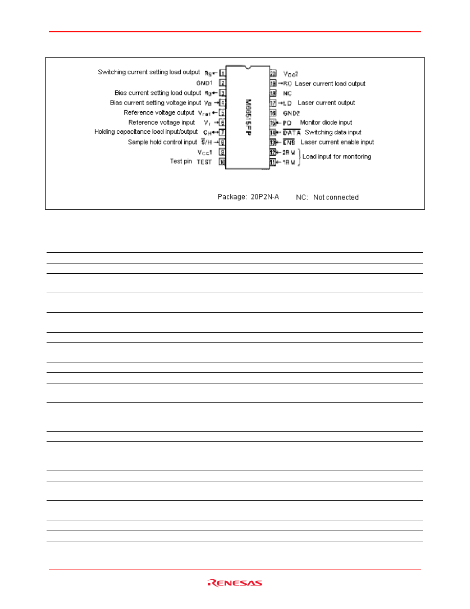
Pin Configuration (top view)
Description of Pin
Pin name
Name
Function
LD
Laser current output
Connected to the semiconductor LD cathode
PD
Monitor diode input
Connected to the monitor PD anode
R
S
Switching current setting load
output
Connects the load resistance to set the current for switching (I
SW
) to GND
R
B
Bias current setting load
output
Connects the load resistance to set the bias current (I
B
) to GND. If I
B
is not
used, this pin should be left open.
V
B
Bias current setting voltage
input
The bias current value (I
B
) can be set by applying a voltage to this pin. If I
B
is not used, this pin should be left open.
DATA
Switching data input
At "L", the current I
SW
+I
B
flows to the LD; at "H", the current to the LD is I
B
1RM, 2RM
Load input for monitoring
Connect a load resistance to convert the monitor PD current to a voltage
across 1RM and 2RM
ENB
Laser current enable input
When "H", all current source circuits are turned off
RO
Laser current load output
Connect a laser current load resistance between this pin and V
CC
S/H
Sample hold control input
When "L", sample (APC) operation is performed; when "H", hold
(switching) is performed
CH
Hold capacitor load
input/output
Connect a hold capacitor between this pin and GND. This pin is connected
within the M66515 to the sample hold circuit output and I
SW
current source
input.
Vref
Reference voltage output
Output pin for the M66515 internal reference voltage (1.2 V typ)
Vr
Reference voltage input
A reference voltage is applied to cause operation of the comparator within
the sample hold circuit. When using the reference voltage within the
M66515, this pin should be connected to the V
ref
pin.
TEST
Test pin
Pin used for testing at time of shipment of the M66515; should be left open
V
CC
1
Power supply pin 1
Power supply for the internal analog system; connect to a positive power
supply (+5 V)
V
CC
2
Power supply pin 2
Power supply for the internal digital system; connect to a positive power
supply (+5 V)
GND1
GND pin 1
GND for internal analog system
GND2
GND pin 2
GND for internal digital system
M66515FP
Rev.1.00, Sep.22.2003, page 3 of 11
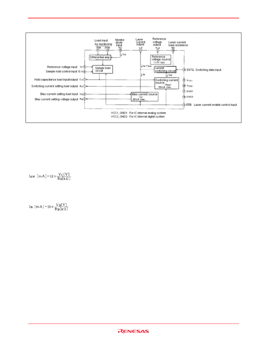
Block Diagram
Explanation of operation
1. Laser driving current values
The values of the laser driving currents I
SW
and I
B
can be approximated as follows, if V
C
is the voltage of the hold
capacitor connected to the C
H
pin.
(1) I
SW
(switched current)
Here 0
≤
V
C
≤
V
CC
-1.8 V, I
SW
(max) =120 mA, and R
S
is the value of the resistance connected between the R
S
pin and
GND
(2) I
B
(bias current)
Here 0
≤
V
B
≤
V
CC
-2.7 V, I
B
(max) =30 mA, and R
B
is the value of the resistance connected between the R
B
pin and GND
2. Switching operation
When
DATA="L", the LD driving current is I
SW
+I
B
; when
DATA="H", the LD driving current is I
B
.
3.
ENB input
Whereas the laser driving current is controlled by
DATA input by controlling the driving current applied to the laser
with the current source in the M66515 turned on, control by
ENB turns the current source operation on and off.
When
ENB="L" the current source is turned on, and when ENB="H" the current source is turned off.
When
ENB="H", the C
H
pin is forced to "L" level, and the charge on the capacitor connected to the C
H
pin is forcibly
discharged.
4. Internal reset operation
The M66515 incorporates a reset circuit to prevent the flow of excessive current to the laser when power is turned on;
when V
CC
<3.5 V (typ), the internal current source is turned off and the C
H
pin is forced to "L" level.
M66515FP
Rev.1.00, Sep.22.2003, page 4 of 11
5. RO pin
The RO pin is connected to the laser driving current load resistance; current essentially equal to I
SW
flows from this pin.
The load resistance is connected between this pin and V
CC
; by this means the Power dissipation within the IC is
reduced.
However, the circuit operation requires that the voltage at this pin be 2.5 V or above. Hence if the maximum value of
I
SW
is I
SW
(max), then the maximum value RO(max) of the load resistance RO is as follows.
For example, if V
CC
(min)=4.75 V and I
SW
(max)=120 mA, then RO(max)=18.8
Ω
. In other words, when setting the
resistance R
S
such that the maximum value of I
SW
is 120 mA, RO should be 18.8
Ω
or lower.
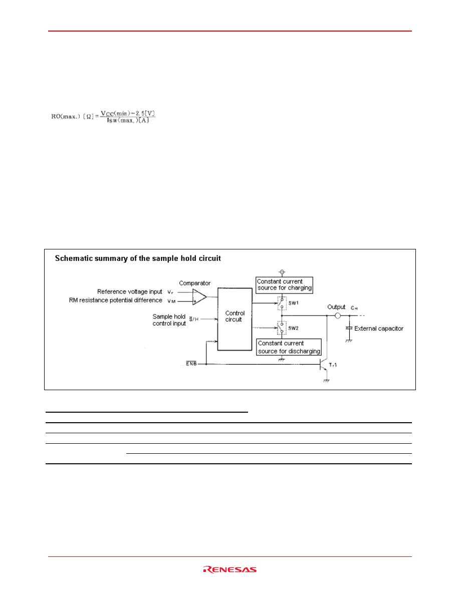
6. Sample-and-hold circuit
(1) Summary of circuit operation
The following is a summary of operation of the sample hold circuit within the M66515.
A PD current arising upon LD light emission flows through the resistance connected between 1RM and 2RM, giving
rise to a potential difference (V
M
). This V
M
is compared with the voltage applied to the pin V
r
, and if V
M
<V
r
, pin C
H
is
a constant current source which charges the external capacitor. If V
M
>V
r
, pin C
H
is a constant current sink which
discharges the external capacitor. This operation is performed when the
S /H input is "L" (sample); when the S/H input
is "H", the C
H
pin is kept in the high-impedance state (hold), regardless of V
M
, V
r
, and the
DATA input state.
Function table
Input
Switched state
ENB
S/H
Vm, Vr
SW1
SW2
Tr1
Output
H
X
X
OFF
OFF
ON
Fixed at "L"
L
H
X
OFF
OFF
OFF
High-impedance state (hold)
L
L
V
M
< Vr
ON
OFF
OFF
Constant current source (sample)
V
M
> Vr
OFF
ON
OFF
Constant current sink (sample)
X: arbitrary
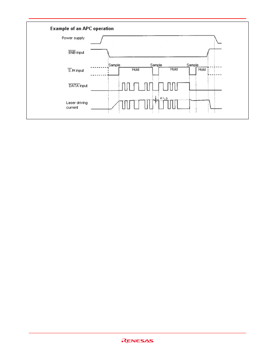
(2) APC operation timing chart
An example of an APC operation timing chart for a given sample hold control signal is shown below.
In this example, a case is shown in which it is assumed that the direction of the leakage current of the C
H
pin in the hold
state is the direction flowing out from the M66515 (the negative direction).
M66515FP
Rev.1.00, Sep.22.2003, page 5 of 11
7. V
CC
and GND pins
The V
CC
1 and V
CC
2 pins and the GND1 and GND2 pins are related to the power supply. The internal circuitry
connected to these pins is as follows.
V
CC
1, GND1: Connected to analog circuitry
V
CC
2, GND2: Connected to digital circuitry
The following should be taken into account in designing the actual wiring.
(1) Wiring widths should be as broad as possible, and drawn-out lengths of wiring should be avoided.
(2) The electrolytic capacitor for voltage stability should be positioned close to V
CC
1 and GND1.
(3) The bypass capacitor should be positioned close to V
CC
2 and GND2.
Important Information Regarding Peripheral Element Wiring
Peripheral elements necessary for M66515 operation should be positioned as close to the M66515 as possible.
Method of Calculating Power dissipation
The M66515 Power dissipation P is essentially given by the following formula.
P = I
CC
×
V
CC
+ I
(RO)
×
I
(RO)
+ I
(LD)
×
V
(LD)
Here V
(RO)
is the RO pin voltage, V
(LD)
is the LD pin voltage, I
(RO)
is the RO pin load current, and I
(LD)
is the LD pin
load current.
For example, when V
CC
= 5.25 V, V
(RO)
= V
(LD)
= 2.5 V, and I
(RO)
= I
(LD)
= 150 mA, the Power dissipation when the laser
is turned on and off is as follows.
(1) When the laser is on (
DATA = “L”, I
CC
= 75 mA):
P
ON
= 75
×
5.25 + 0 + 150
×
2.5 = 768.8 (mW)
(2) When the laser is off (
DATA = “H”, I
CC
= 74 mA):
P
OFF
= 74
×
5.25 + 0 + 150
×
2.5 = 763.5 (mW)

M66515FP
Rev.1.00, Sep.22.2003, page 6 of 11
Absolute Maximum Ratings
(Unless otherwise noted, Ta = –20 to 70°C)
Symbol
Parameter
Conditions
Value
Unit
V
CC
Power supply voltage
−
0.5 to +7.0
V
V
I
Input voltage
CH, Vr
−
0.3 to V
CC
V
DATA, ENB, S/H
−
0.3 to +7.0
V
V
O
Output voltage
RO
−
0.5 to +7.0
V
I
SW
Switching current
150
mA
I
B
Bias current
45
mA
Pd
Power dissipation
Mounted on board, with
Ta=25°C (see note)
1200
mW
Tstg
Storage temperature
−
60 to +150
°
C
Note: When Ta
≥
25°C, derating at 9.6 mW/°C should be performed.
Recommended Operating Conditions
(Unless otherwise noted, Ta = –20 to 70°C)
Limits
Symbol
Parameter
Min
Typ
Max
Unit
V
CC
Power supply voltage
4.75
5.0
5.25
V
I
SW
Switching current
120
mA
I
B
Bias current
30
mA
Topr
Operating ambient temperature
−
20
70
°
C

M66515FP
Rev.1.00, Sep.22.2003, page 7 of 11
Electrical Characteristics
(Unless otherwise noted, V
CC
= 5 V
±
5%, Ta = –20 to 70°C)
Limits
Sym-
bol
Parameter
Measurement conditions
Min
Typ
Max
Unit
Mea-
sure-
ment
cir-
cuit
V
IH
"H" input
voltage
DATA, ENB, S/H
2.0
V
V
IL
"L" input voltage
DATA, ENB, S/H
0.8
V
Vr
Reference
voltage input
Vr
0.4
2.0
V
Vref
I
O
= –10
µ
A
1.2
V
Ta = –20 to 25
°
C
–0.9
Vref
Reference
voltage output
Temperature
coefficient
Ta = 25 to 70
°
C
–0.9
mV/
°
C
1
V
LD
Operating
voltage range
LD
2.5
V
CC
V
V
I
Effective
voltage upper
limit
C
H
V
CC
–
1.8
V
CC
–
1.4
V
V
OH
"H" output
voltage
C
H
ENB = 0.8 V, I
OH
= –2 mA
4.0
V
1
V
OL
"L" output
voltage
C
H
ENB = 0.8 V, I
OL
= 2 mA
0.6
V
1
V
I
= 2.7 V
20
µ
A
DATA, ENB
V
I
= 0.4 V
–0.2
mA
I
L
Input current
C
H
V
I
= 0 to V
CC
±
1
µ
A
CH = 3.0 V, Rs = 360
Ω
, V
LD
= 2 V
120
mA
I
SW
Switching
current (see
note)
LD
Temperature
coefficient
Ta = 20 to 70
°
C
0.11
mA/
°
C
2
I
B
Bias current
(see note)
LD
VB = 1.2 V, RB = 360
Ω
, V
LD
= 2 V
30
mA
2
Icg
Load charging
current
C
H
ENB = 0.8 V, V
O
= 0.6 to 4.0 V
–0.66
–2.0
mA
3
Idg
Load discharge
current
C
H
ENB = 0.8 V, V
O
= 0.6 to 4.0 V
0.66
2.0
mA
3
Ioz
Output current
in off state
C
H
V
O
= 0 to V
CC
, Hold state
±
5
µ
A
3
ENB = 0.8 V, DATA = 2.0 V
0.33
50
I
OFF
Output current
when off
LD
ENB = 2.0 V, DATA = 0.8 V
0.01
50
µ
A
2
DATA =
0 V
54
75
I
CC
Power supply current
V
CC
= 5.25 V,
ENB = 0 V,
C
H
= 3.0 V, V
B
= 1.2 V,
R
S
= 300
Ω
, R
B
= 360
Ω
,
R
O
= LD = 5.0 V
DATA =
4.5 V
52
74
mA
4
*Typical values are for Ta = 25°C, V
CC
= 5 V.
Note:
These quantities indicate the input voltage-output current conversion characteristic; I
SW
and I
B
should be used
within the range of the rated values under recommended operating conditions.
M66515FP
Rev.1.00, Sep.22.2003, page 8 of 11
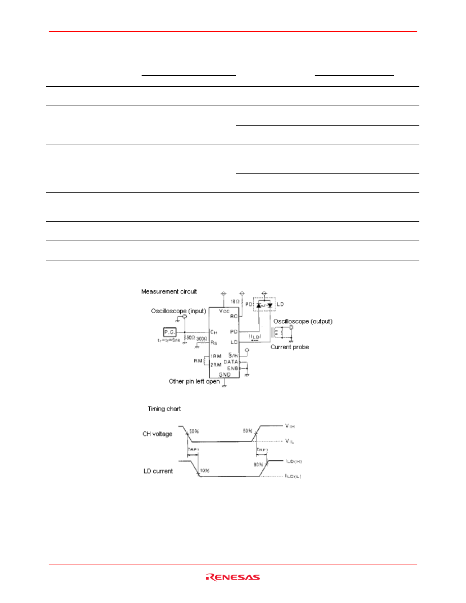
Switching Characteristics
(Ta = 25°C, V
CC
= 5 V)
Measurement pin
Limits
Symbol
Item
Input
Output
Measurement
conditions
Min.
Typ.
Max.
Unit
f
OP
Operating
frequency
40
Mbps
I
LD(L)
= 0 mA
I
LD(H)
= 60 mA (Note 1)
7
µ
s
t
RP1
Circuit response
time 1
C
H
voltage
LD current
I
LD(L)
= 55 mA
I
LD(H)
= 65 mA (Note 1)
2
µ
s
I
PD(L)
= 0 mA
I
PD(H)
= 2 mA
RM = 1 k
Ω
(Note 2)
15
µ
s
t
RP2
Circuit response
time 2
PD current
C
H
voltage
|
∆
I
PD
| = 0.2 mA
RM = 1 k
Ω
(Note 2)
8
µ
s
t
RP3
Circuit response
time 3
S/H voltage
C
H
voltage
I
PD
= 0 mA, 2 mA
RM = 1 k
Ω
, Vr = 1.2 V
(Note 3)
1
µ
s
t
ON
Circuit turn-on
time
ENB voltage
LD current
I
LD(H)
= 60 mA (Note 4)
5
µ
s
t
OFF
Circuit turn-off
time
ENB voltage
LD current
I
LD(H)
= 60 mA (Note 4)
2
µ
s
Note 1. Measurement circuit and Timing chart
M66515FP
Rev.1.00, Sep.22.2003, page 9 of 11
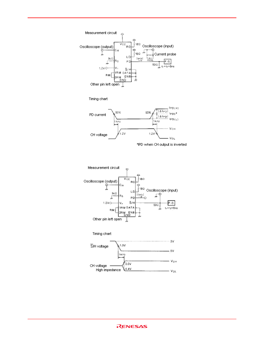
Note 2. Measurement circuit and Timing chart
Note 3. Measurement circuit and Timing chart
M66515FP
Rev.1.00, Sep.22.2003, page 10 of 11
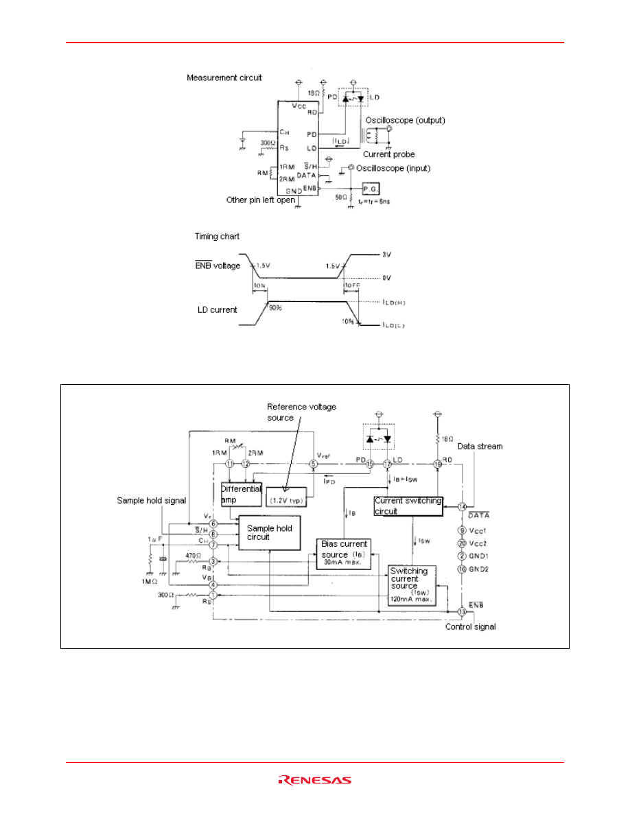
Note 4. Measurement circuit and Timing chart
Application example
M66515FP
Rev.1.00, Sep.22.2003, page 11 of 11
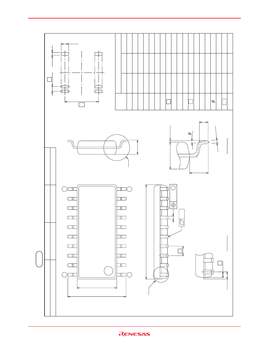
Package Dimensions
SOP20-P-300-1.27
W
eight(g)
—
JEDEC Code
0.26
EIAJ P
a
c
kage Code
Lead Mater
ial
Cu Allo
y
20P2N-A
Plastic 20pin 300mil SOP
Symbol
Min
Nom
Max
A
A
2
b
c
D
E
L
L
1
y
Dimension in Millimeters
H
E
A
1
I
2
—
—
.35
0
0
.18
0
.5
12
.2
5
—
.5
7
.4
0
—
—
—
—
.27
1
.1
0
—
.8
1
.4
0
.2
0
.6
12
.3
5
.27
1
.8
7
.6
0
.25
1
—
—
.62
7
—
.2
0
.1
2
—
.5
0
.25
0
.7
12
.4
5
—
.1
8
.8
0
—
.1
0
—
b
2
0.76
—
0
°
8
°
e
e
1
20
11
10
1
H
E
E
D
e
y
F
A
A
2
A
1
L
1
L
c
e
b
2
e
1
I
2
Recommended Mount P
a
d
Detail F
Detail G
z
Z
1
x
—
—
Z
1
—
0.585
—
—
—
—
0.735
0.25
z
b
x
M
G
MMP
© 2003. Renesas Technology Corp., All rights reserved. Printed in Japan.
Colophon 1.0
Keep safety first in your circuit designs!
1. Renesas Technology Corp. puts the maximum effort into making semiconductor products better and more reliable, but there is always the possibility that trouble
may occur with them. Trouble with semiconductors may lead to personal injury, fire or property damage.
Remember to give due consideration to safety when making your circuit designs, with appropriate measures such as (i) placement of substitutive, auxiliary
circuits, (ii) use of nonflammable material or (iii) prevention against any malfunction or mishap.
Notes regarding these materials
1. These materials are intended as a reference to assist our customers in the selection of the Renesas Technology Corp. product best suited to the customer's
application; they do not convey any license under any intellectual property rights, or any other rights, belonging to Renesas Technology Corp. or a third party.
2. Renesas Technology Corp. assumes no responsibility for any damage, or infringement of any third-party's rights, originating in the use of any product data,
diagrams, charts, programs, algorithms, or circuit application examples contained in these materials.
3. All information contained in these materials, including product data, diagrams, charts, programs and algorithms represents information on products at the time of
publication of these materials, and are subject to change by Renesas Technology Corp. without notice due to product improvements or other reasons. It is
therefore recommended that customers contact Renesas Technology Corp. or an authorized Renesas Technology Corp. product distributor for the latest product
information before purchasing a product listed herein.
The information described here may contain technical inaccuracies or typographical errors.
Renesas Technology Corp. assumes no responsibility for any damage, liability, or other loss rising from these inaccuracies or errors.
Please also pay attention to information published by Renesas Technology Corp. by various means, including the Renesas Technology Corp. Semiconductor
home page (http://www.renesas.com).
4. When using any or all of the information contained in these materials, including product data, diagrams, charts, programs, and algorithms, please be sure to
evaluate all information as a total system before making a final decision on the applicability of the information and products. Renesas Technology Corp. assumes
no responsibility for any damage, liability or other loss resulting from the information contained herein.
5. Renesas Technology Corp. semiconductors are not designed or manufactured for use in a device or system that is used under circumstances in which human life
is potentially at stake. Please contact Renesas Technology Corp. or an authorized Renesas Technology Corp. product distributor when considering the use of a
product contained herein for any specific purposes, such as apparatus or systems for transportation, vehicular, medical, aerospace, nuclear, or undersea repeater
use.
6. The prior written approval of Renesas Technology Corp. is necessary to reprint or reproduce in whole or in part these materials.
7. If these products or technologies are subject to the Japanese export control restrictions, they must be exported under a license from the Japanese government and
cannot be imported into a country other than the approved destination.
Any diversion or reexport contrary to the export control laws and regulations of Japan and/or the country of destination is prohibited.
8. Please contact Renesas Technology Corp. for further details on these materials or the products contained therein.
Sales Strategic Planning Div. Nippon Bldg., 2-6-2, Ohte-machi, Chiyoda-ku, Tokyo 100-0004, Japan
http://www.renesas.com
Renesas Technology America, Inc.
450 Holger Way, San Jose, CA 95134-1368, U.S.A
Tel: <1> (408) 382-7500 Fax: <1> (408) 382-7501
Renesas Technology Europe Limited.
Dukes Meadow, Millboard Road, Bourne End, Buckinghamshire, SL8 5FH, United Kingdom
Tel: <44> (1628) 585 100, Fax: <44> (1628) 585 900
Renesas Technology Europe GmbH
Dornacher Str. 3, D-85622 Feldkirchen, Germany
Tel: <49> (89) 380 70 0, Fax: <49> (89) 929 30 11
Renesas Technology Hong Kong Ltd.
7/F., North Tower, World Finance Centre, Harbour City, Canton Road, Hong Kong
Tel: <852> 2265-6688, Fax: <852> 2375-6836
Renesas Technology Taiwan Co., Ltd.
FL 10, #99, Fu-Hsing N. Rd., Taipei, Taiwan
Tel: <886> (2) 2715-2888, Fax: <886> (2) 2713-2999
Renesas Technology (Shanghai) Co., Ltd.
26/F., Ruijin Building, No.205 Maoming Road (S), Shanghai 200020, China
Tel: <86> (21) 6472-1001, Fax: <86> (21) 6415-2952
Renesas Technology Singapore Pte. Ltd.
1, Harbour Front Avenue, #06-10, Keppel Bay Tower, Singapore 098632
Tel: <65> 6213-0200, Fax: <65> 6278-8001
RENESAS SALES OFFICES
Wyszukiwarka
Podobne podstrony:
laser wykresy moje id 263536 Nieznany
laser wykresy moje id 263536 Nieznany
Abolicja podatkowa id 50334 Nieznany (2)
4 LIDER MENEDZER id 37733 Nieznany (2)
katechezy MB id 233498 Nieznany
metro sciaga id 296943 Nieznany
perf id 354744 Nieznany
interbase id 92028 Nieznany
Mbaku id 289860 Nieznany
Probiotyki antybiotyki id 66316 Nieznany
miedziowanie cz 2 id 113259 Nieznany
LTC1729 id 273494 Nieznany
D11B7AOver0400 id 130434 Nieznany
analiza ryzyka bio id 61320 Nieznany
pedagogika ogolna id 353595 Nieznany
Misc3 id 302777 Nieznany
więcej podobnych podstron