
1
Laboratory Exercise 8
Memory Blocks
In computer systems it is necessary to provide a substantial amount of memory. If a
system is implemented using FPGA technology it is possible to provide some amount of
memory by using the memory resources that exist in the FPGA device. If additional memory is
needed, it has to be implemented by connecting external memory. In this exercise we will
examine the general issues involved in implementing such memory.
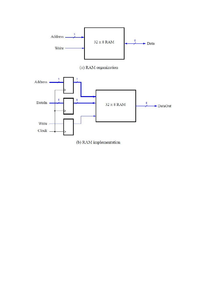
A diagram of the random access memory (RAM) module that we will implement is shown
in Figure 1a. It contains 32 eight-bit words (rows), which are accessed using a five-bit address
port, an eight-bit data port, and a write control input. We will consider two different ways of
implementing this memory: using dedicated memory blocks in an FPGA device, and using a
separate memory chip.
The Cyclone IV 4CE115F29 FPGA that is included on the DE2-115 board provides
dedicated memory resources called M9K blocks. Each M9K block contains 4096 memory
bits, which can be configured to implement memories of various sizes. A common term used to
specify the size of a memory is its aspect ratio, which gives the depth in words and the width in
bits (depth x width). Some aspect ratios supported by the M9K block are 8K x 1, 4K x 2, 2K x 4,
1K x 8, 1K x 9, 512 x 16, and 512 x 18. We will utilize the 1K x 8 mode in this exercise, using
only the first 32 words in the memory. We should also mention that many other modes of
operation are supported in an M9K block, but we will not discuss them here.
2
Figure 1. A 32 x 8 RAM module.
There are two important features of the M9K block that have to be mentioned. First, it
includes registers that can be used to synchronize all of the input and output signals to a clock
input. Second, the M9K block has separate ports for data being written to the memory and data
being read from the memory. A requirement for using the M9K block is that either its input ports,
output port, or both, have to be synchronized to a clock input. Given these requirements, we
will implement the modified 32 x 8 RAM module shown in Figure 1b. It includes registers for
the address, data input, and write ports, and uses a separate unregistered data output port.
Part I
Commonly used logic structures, such as adders, registers, counters and memories, can
be implemented in an FPGA chip by using LPM modules from the Quartus II Library of
Parameterized Modules. Altera recommends that a RAM module be implemented by using the
RAM:1-PORT LPM. In this exercise you are to use this LPM to implement the memory module
in Figure 1b.
1. Create a new Quartus II project to implement the memory module. Select as the
target chip the Cyclone IV EP4CE115F29C8, which is the FPGA chip on the Altera
DE2-115 board.
2. You can learn how the Mega-Wizard Plug-in Manager is used to generate a desired
LPM module by reading the tutorial Using Library Modules in VHDL Designs. This
tutorial is provided in the University Program section of Altera’s web site. In the first
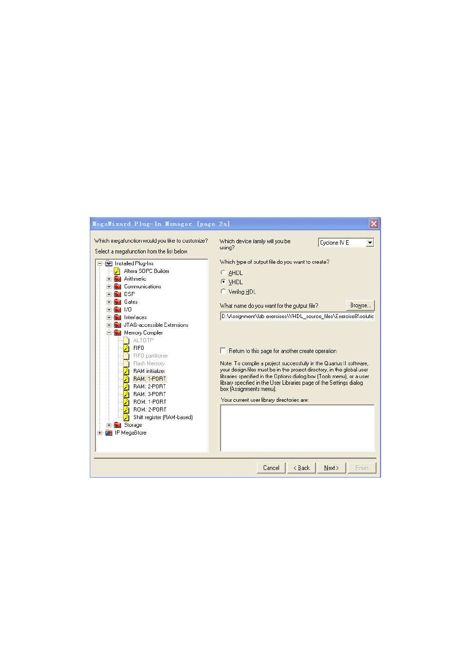
3
screen of the MegaWizard Plug-in Manager choose the RAM:1-PORT LPM, which is
found under the Memory Compiler category. As indicated in Figure 2, select VHDL HDL
as the type of output file to create, and give the file the name ramlpm.vhd. On the next
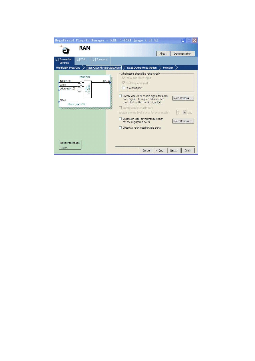
page of the Wizard specify a
memory size of 32 eight-bit words, and select M9K as the type of RAM block. Advance
to the subsequent page and accept the default settings to use a single clock for the
RAM’s registers, and then advance again to the page shown in Figure 3. On this page
deselect the setting called Read output port(s) under the category Which ports should be
registered?. This setting creates a RAM module that matches the structure in Figure 1b,
with registered input ports and unregistered output ports. Accept defaults for the rest of
the settings in the Wizard, and then instantiate in your top-level VHDL file the entity
generated in ramlpm.vhd. Include appropriate input and output signals in your VHDL
code for the memory ports given in Figure 1b.
Figure 2. Choosing the RAM:1-PORT LPM.
4
Figure 3. Configuring input and output ports on the RAM:1-PORT LPM.
3. Compile the circuit. Observe in the Compilation Report that the Quartus II Compiler
uses 256 bits in one of the M9K memory blocks to implement the RAM circuit.
4. Simulate the behavior of your circuit and ensure that you can read and write data in
the memory.
Part II
Now, we want to realize the memory circuit in the FPGA on the DE2-115 board, and use
toggle switches to load some data into the created memory. We also want to display the
contents of the RAM on the 7-segment displays.
1. Make a new Quartus II project which will be used to implement the desired circuit on
the DE2-115 board.
2. Create another VHDL file that instantiates the ramlpm
module and that includes
the required input and output pins on the DE2-115 board. Use toggle switches SW 7−0
to input a byte of data into the RAM location identified by a 5-bit address specified
with toggle switches SW15−11. Use SW17 as the Write signal and use KEY0 as
the
Clock input. Display the value of the Write signal on LEDG 0. Show the address value on
the 7-segment displays HEX7 and HEX6, show the data being input to the memory on
HEX5 and HEX4, and show the data read out of the memory on HEX1 and HEX0.
3. Test your circuit and make sure that all 32 locations can be loaded properly.

5
Part III
Instead of directly instantiating the LPM module, we can implement the required memory
by specifying its structure in the VHDL code. In a VHDL-specified design it is possible to define
the memory as a multidimensional array. A 32 x 8 array, which has 32 words with 8 bits per
word, can be declared by the statements
TYPE mem IS ARRAY(0 TO 31) OF STD LOGIC VECTOR(7 DOWNTO 0);
SIGNAL memory array : mem;
In the Cyclone IV FPGA, such an array can be implemented either by using the flip-flops
that each logic element contains or, more efficiently, by using the M9K blocks. There are two
ways of ensuring that the M9K blocks will be used. One is to use an LPM module from the
Library of Parameterized Modules, as we saw in Part I. The other is to define the memory
requirement by using a suitable style of VHDL code from which the Quartus II compiler can
infer that a memory block should be used. Quartus II Help shows how this may be done with
examples of VHDL code (search in the Help for “Inferred memory”).
Perform the following steps:
1. Create a new project which will be used to implement the desired circuit on the
DE2-115 board.
2. Write a VHDL file that provides the necessary functionality, including the ability to load
the RAM and read its contents as done in Part II.
3. Assign the pins on the FPGA to connect to the switches and the 7-segment displays.
4. Compile the circuit and download it into the FPGA chip.
5. Test the functionality of your design by applying some inputs and observing the output.
Describe any differences you observe in comparison to the circuit from Part II.
Part IV
The DE2-115 board includes an SRAM chip, called IS61WV102416BLL-10, which is a
static RAM having a capacity of 2M 16-bit words. The SRAM interface consists of an 20-bit
address port, A 19−0, and a 16-bit bidirectional data port, I/O15−0. It also has several control
inputs, CE, OE, W E, UB, and LB, which are described in Table 1
Name
Purpose
CE#
Chip enable−asserted low during all SRAM operations
OE#
Output enable−can be asserted low during only read operations, or during all
operations
WE#
Write enable−asserted low during a write operation
UB#
Upper byte−asserted low to read or write the upper byte of an address
LB#
Lower byte−asserted low to read or write the lower byte of an address
Table 1. SRAM control inputs.
6
The operation of the IS61WV102416BLL chip is described in its data sheet, which can
obtained from the DE2-115 system CD that is included with the DE2-115 board, or by
performing an Internet search. The data sheet describes a number of modes of operation of
the memory and lists many timing parameters related to its use. For the purposes of this
exercise a simple operating mode is to always assert (set to 0) the control inputs CE, OE, UB,
and LB, and then to control reading and writing of the memory by using only the W E input.
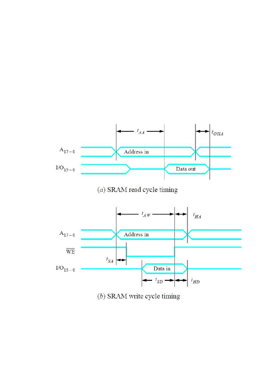
Simplified timing diagrams that correspond to this mode are given in Figure 4. Part (a) shows a
read cycle, which begins when a valid address appears on A19−0 and the W E input is not
asserted. The memory places valid data on the I/O15−0 port after the address access delay,
tAA. When the read cycle ends because of a change in the address value, the output data
remains valid for the output hold time, t OHA.
Figure 4. SRAM read and write cycles.
Figure 4b gives the timing for a write cycle. It begins when W E is set to 0, and it ends
when W E is set back to 1. The address has to be valid for the address setup time, tAW, and
the data to be written has to be valid for the data setup time, tSD, before the rising edge of W E.
Table 2 lists the minimum and maximum values of all timing parameters shown in Figure 4.

7
Parameter
Min
Max
tAA
−
10 ns
tOHA
2.5 ns
−
tAW
8 ns
−
tSD
6 ns
−
tHA
0
−
tSA
0
−
tHD
0
−
Table 2. SRAM timing parameter values
You are to realize the 32 x 8 memory in Figure 1a by using the SRAM chip. It is a good
approach to include in your design the registers shown in Figure 1b, by implementing these
registers in the FPGA chip. Be careful to implement properly the bidirectional data port that
connects to the memory.
1. Create a new Quartus II project for your circuit. Write a VHDL file that provides the
necessary functionality, including the ability to load the memory and read its contents.
Use the same switches, LEDs, and 7-segment displays on the DE2-115 board as in
Parts II and III, and use the SRAM pin names shown in Table 3 to interface your circuit to
the IS61WV102416BLL chip (the SRAM pin names are also given in the DE2-115 User
Manual).
Note that you will not use all of the address and data ports on the IS61WV102416BLL
chip for your 32 x 8 memory; connect the unneeded ports to 0 in your VHDL entity.
SRAM port name
DE2-115 pin name
A
19−0
SRAM ADDR
19−0
I/O
15−0
SRAM DQ
15−0
CE#
SRAM CE N
OE#
SRAM OE N
WE#
SRAM WE N
UB#
SRAM UB N
LB#
SRAM LB N
Table 3. DE2-115 pin names for the SRAM chip.
2. Compile the circuit and download it into the FPGA chip.
3. Test the functionality of your design by reading and writing values to several different
memory locations.
Part V
The SRAM block in Figure 1 has a single port that provides the address for both read and
write operations. For this part you will create a different type of memory module, in which there
is one port for supplying the address for a read operation, and a separate port that gives the
address for a write operation. Perform the following steps.
8
1. Create a new Quartus II project for your circuit. To generate the desired memory
module open the Mega-Wizard Plug-in Manager and select again the RAM:2-PORT
LPM in the storage category. On Page 1 of the Wizard choose the setting With one read
port and one write port (simple dual-port mode) in the category called How will you be
using the dual port ram?. Advance through Pages 2 to 5 and make the same choices as
in Part II. On Page 6 choose the setting I don’t care in the category Mixed Port
Read-During-Write for Single Input Clock RAM. This setting specifies that it does not
matter whether the memory outputs the new data being written, or the old data
previously stored, in the case that the write and read addresses are the same. Page 8 of
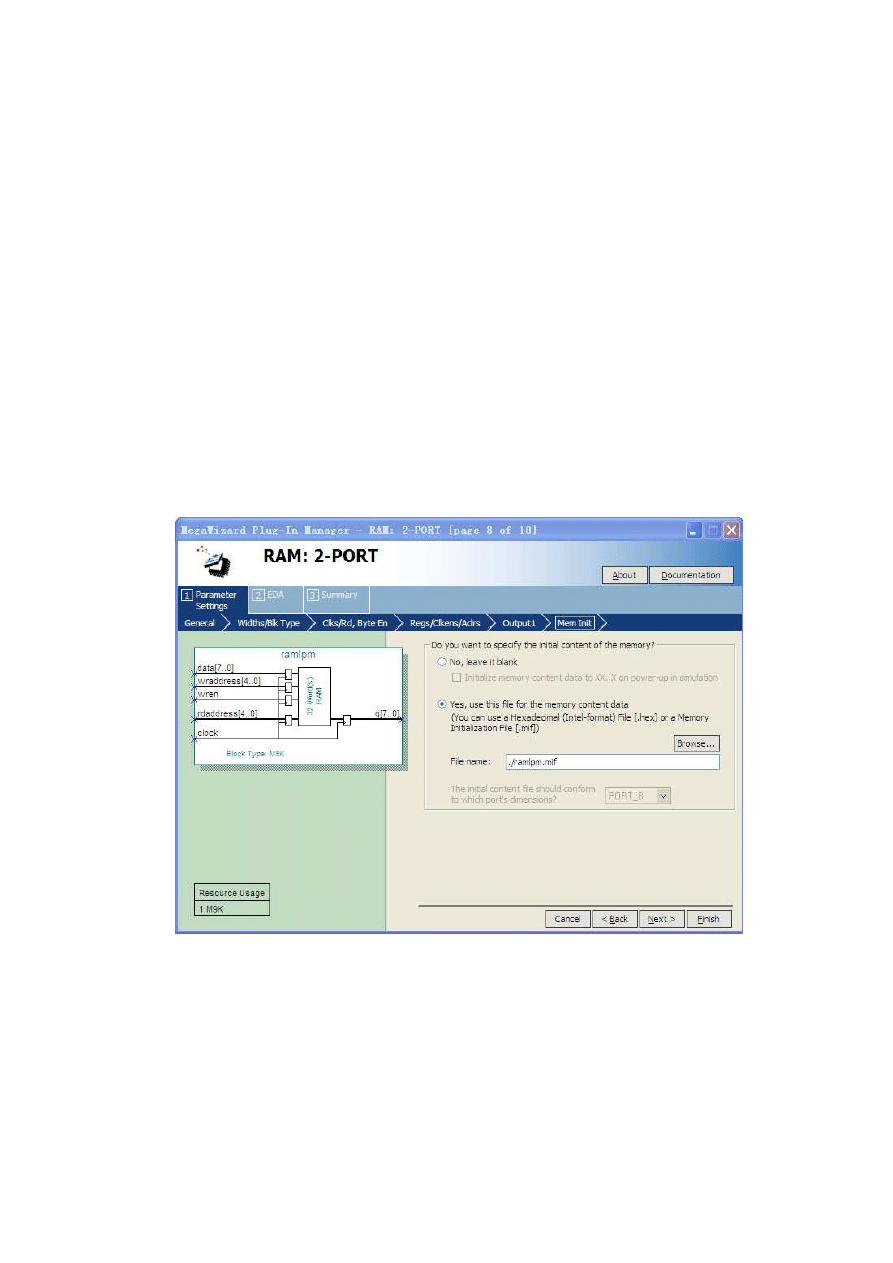
the Wizard is displayed in Figure 5. It makes use of a feature that allows the memory
module to be loaded with initial data when the circuit is programmed into the FPGA chip.
As shown in the figure, choose the setting Yes, use this file for the memory content data,
and specify the filename ramlpm.mif. To learn about the format of a memory initialization
file (MIF), see the Quartus II Help. You will need to create this file and specify some data
values to be stored in the memory. Finish the Wizard and then examine the generated
memory module in the file ramlpm.vhd.
Figure 5. Specifying a memory initialization file (MIF).
2. Write a VHDL file that instantiates your dual-port memory. To see the RAM contents,
add to your design a capability to display the content of each byte (in hexadecimal
format) on the 7-segment displays HEX1 and HEX0. Scroll through the memory
locations by displaying each byte for about one second. As each byte is being displayed,
show its address (in hex format) on the 7-segment displays HEX3 and HEX2. Use the 50
MHz clock, OSC_ 50(0), on the DE2-115 board, and use KEY 0 as a reset input. For the
9
write address and corresponding data use the same switches, LEDs, and 7-segment
displays as in the previous parts of this exercise. Make sure that you properly
synchronize the toggle switch inputs to the 50 MHz clock signal.
3. Test your circuit and verify that the initial contents of the memory match your
ramlpm.mif file. Make sure that you can independently write data to any address by
using the toggle switches.
Part VI
The dual-port memory created in Part V allows simultaneous read and write operations to
occur, because it has two address ports. In this part of the exercise you should create a similar
capability, but using a single-port RAM. Since there will be only one address port you will need
to use multiplexing to select either a read or write address at any specific time. Perform the
following steps.
1. Create a new Quartus II project for your circuit, and use the MegaWizard Plug-in
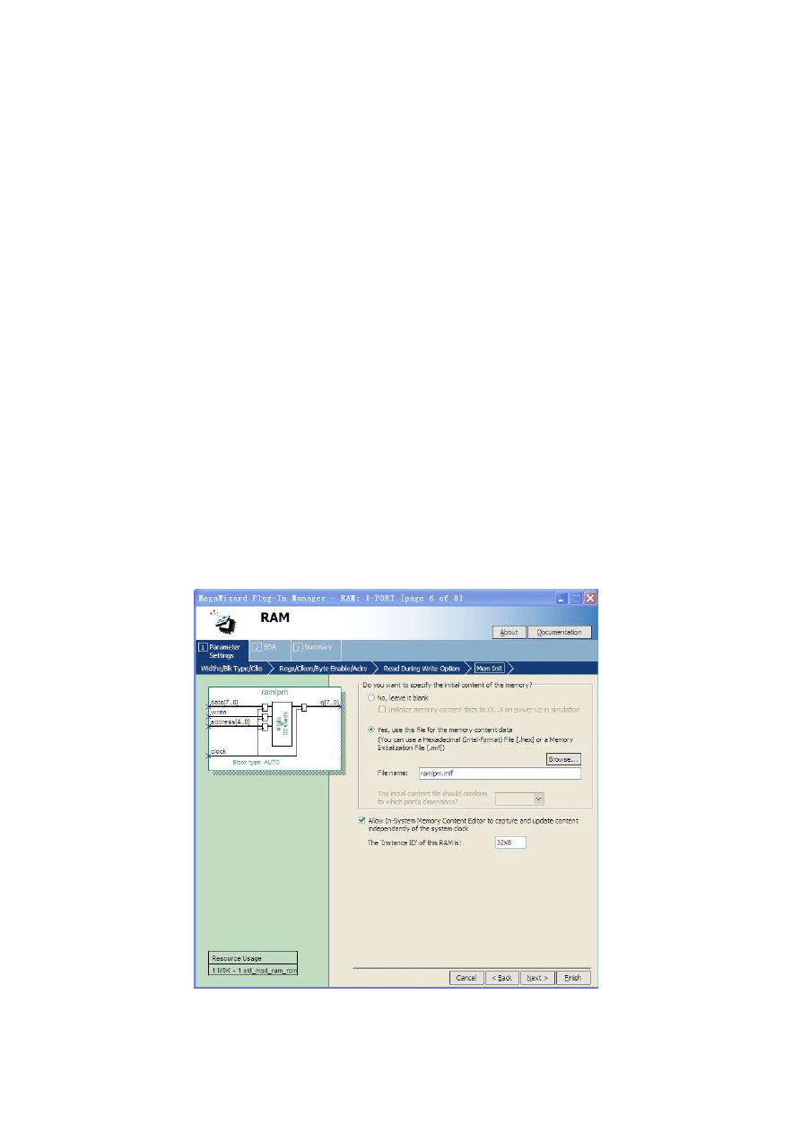
Manager to again create a single-port version of the RAM:1-PORT LPM. For Pages 1 to
6 of the Wizard use the same settings as in Part I. On Page 6, shown in Figure 6, specify
the ramlpm.mif file as you did in Part V, but also make the setting Allow In-System
Memory Content Editor to capture and update content independently of the system clock.
This option allows you to use a feature of the Quartus II CAD system called the
In-System Memory Content Editor to view and manipulate the contents of the created
RAM module. When using this tool you can optionally specify a four-character ‘Instance
ID’ that serves as a name for the memory; in Figure 7 we gave the RAM module the
name 32x8. Complete the final steps in the Wizard.
Figure 6. Configuring RAM:1-PORT for use with the In-System Memory Content Editor.
10
2. Write a VHDL file that instantiates your memory module. Include in your design the
ability to scroll through the memory locations as in Part V. Use the same switches, LEDs,
and 7-segment displays as you did previously.
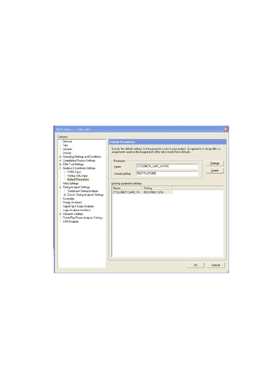
3. Before you can use the In-System Memory Content Editor tool, one additional setting
has to be made. In the Quartus II software select Assignments > Settings to open the
window in Figure 7, and then open the item called Default Parameters under Analysis
and Synthesis Settings. As shown in the figure, type the parameter name CYCLONEIV
SAFE WRITE and assign the value RESTRUCTURE. This parameter allows the
Quartus II synthesis tools to modify the single-port RAM as needed to allow reading and
writing of the memory by the In-System Memory Content Editor tool. Click OK to exit
from the Settings window.
Figure 7. Setting the CYCLONEIV SAFE WRITE parameter.
4. Compile your code and download the circuit onto the DE2-115 board. Test the circuit’s
operation and ensure that read and write operations work properly. Describe any
differences you observe from the behavior of the circuit in Part V.
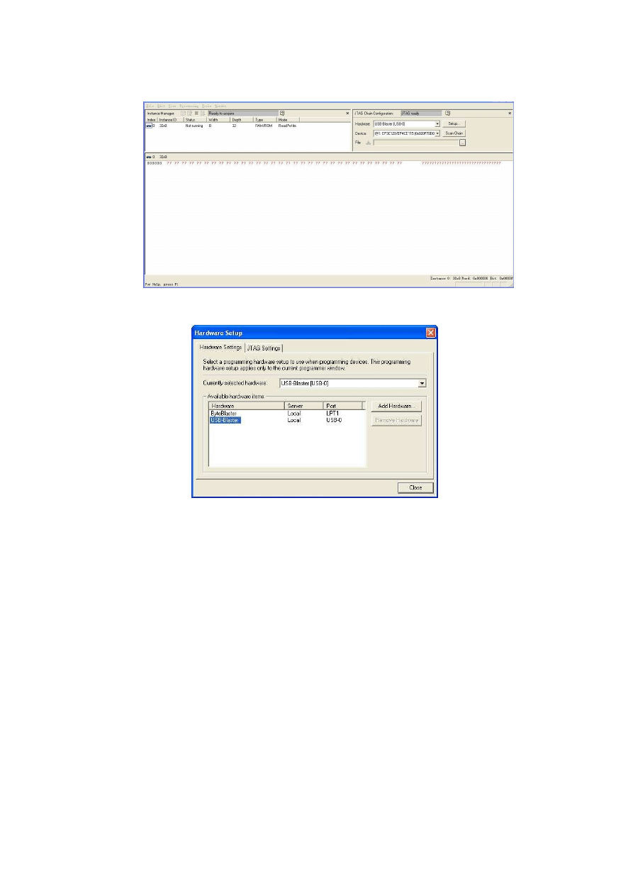
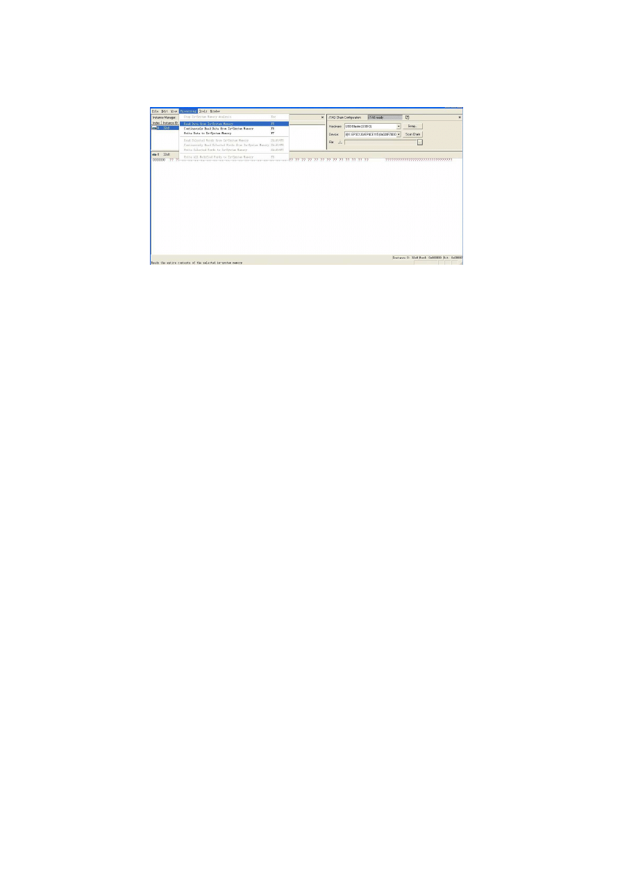
5. Select Tools > In-System Memory Content Editor, which opens the window in Figure 8.
To specify the connection to your DE2-115 board click on the Setup button on the right
side of the screen. In the window in Figure 9 select the USB-Blaster hardware, and then
close the Hardware Setup dialog.
11
Figure 8. The In-System Memory Content Editor window.
Figure 9. The Hardware Setup window.
Instructions for using the In-System Memory Content Editor tool can be found in the
Quartus II Help. A simple operation is to right-click on the 32x8 memory module, as indicated
in Figure 10, and select Read Data from In-System Memory. This action causes the contents
of the memory to be displayed in the bottom part of the window. You can then edit any of the
displayed values by typing over them. To actually write the new value to the RAM, right click
again on the 32x8 memory module and select Write All Modified Words to In-System Memory.
Experiment by changing some memory values and observing that the data is properly
displayed both on the 7-segment displays on the DE2-115 board and in the In-System Memory
Content Editor window.
12
Figure 10. Using the In-System Memory Content Editor tool.
Part VII
For this part you are to modify your circuit from Part VI (and Part IV) to use the
IS61WV102416BLL SRAM chip instead of an M9K block. Create a Quartus II project for the
new design, compile it, download it onto the DE2-115 boards, and test the circuit.
In Part VI you used a memory initialization file to specify the initial contents of the 32 x 8
RAM block, and you used the In-System Memory Content Editor tool to read and modify this
data. This approach can be used only for the memory resources inside the FPGA chip. To
perform equivalent operations using the external SRAM chip you can use a special capability
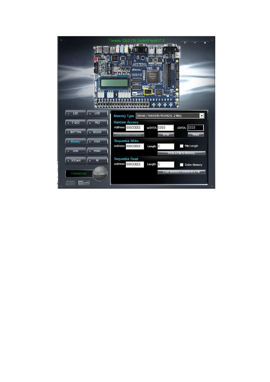
of the DE2-115 board called the DE2-115 Control Panel. Chapter 3 of the DE2-115 User
Manual shows how to use this tool. The procedure involves programming the FPGA with a
special circuit that communicates with the Control Panel software application, which is
illustrated in Figure 11, and using this setup to load data into the SRAM chip. Subsequently,
you can reprogram the FPGA with your own circuit, which will then have access to the data
stored in the SRAM chip (reprogramming the FPGA has no effect on the external memory).
Experiment with this capability and ensure that the results of read and write operations to the
SRAM chip can be observed both in the your circuit and in the DE2-115 Control Panel
software.
13
Figure 11. The DE2-115 Control Panel software.
Copyright
○
c
2010 Altera Corporation.
Wyszukiwarka
Podobne podstrony:
Introduction to VHDL
lab1 VHDL
lab8(1) id 260269 Nieznany
[8]konspekt new, Elektrotechnika AGH, Semestr II letni 2012-2013, Fizyka II - Laboratorium, laborki,
Rafał Polak 12k2 lab8, Inżynieria Oprogramowania - Informatyka, Semestr III, Systemy Operacyjne, Spr
sprawko modelowanie?p lab8 g3
lab8 przyklad
Lab8 occ id 260283 Nieznany
lab8 1 uklady rownan liniowych
P J Ashenden VHDL tutorial
cw8 wyniki, Elektrotechnika AGH, Semestr II letni 2012-2013, Fizyka II - Laboratorium, laborki, labo
lab8 listing
lab8 AC
VHDL(1)
8 opracowanie, Elektrotechnika AGH, Semestr II letni 2012-2013, Fizyka II - Laboratorium, laborki, l
ELC VHDL
Język opisu sprzętu VHDL (K Kołek) vhdl ksiazka
lab8, 3.2.2.4 Packet Tracer - Configuring Trunks Instructions
więcej podobnych podstron