
Molecular Doping of Graphene
T. O. Wehling,*
,†
K. S. Novoselov,
‡
S. V. Morozov,
§
E. E. Vdovin,
§
M. I. Katsnelson,
|
A. K. Geim,
‡
and A. I. Lichtenstein
†
1st Institute for Theoretical Physics, Hamburg UniVersity, Jungiusstrasse 9,
D-20355 Hamburg, Germany, School of Physics and Astronomy, UniVersity of
Manchester, M13 9PL, Manchester, U.K., Institute for Microelectronics Technology,
142432 ChernogoloVka, Russia, and Institute for Molecules and Materials, Radboud
UniVersity of Nijmegen, ToernooiVeld 1, 6525 ED Nijmegen, The Netherlands
Received September 14, 2007; Revised Manuscript Received November 20, 2007
ABSTRACT
Graphene is considered as one of the most promising materials for post silicon electronics, as it combines high electron mobility with atomic
thickness [Novoselov et al.
Science 2004, 306, 666
−
669. Novoselov et al.
Proc. Natl. Acad. Sci. U.S.A. 2005, 102, 10451
−
10453]. The possibility
of chemical doping and related excellent chemical sensor properties of graphene have been demonstrated experimentally [Schedin et al.
Nat.
Mater. 2007, 6, 652
−
655], but a microscopic understanding of these effects has been lacking, so far. In this letter, we present the first joint
experimental and theoretical investigation of adsorbate-induced doping of graphene. A general relation between the doping strength and
whether adsorbates are open- or closed-shell systems is demonstrated with the NO
2
system: The single, open shell NO
2
molecule is found
to be a strong acceptor, whereas its closed shell dimer N
2
O
4
causes only weak doping. This effect is pronounced by graphene’s peculiar
density of states (DOS), which provides an ideal situation for model studies of doping effects in semiconductors. We show that this DOS is
ideal for “chemical sensor” applications and explain the recently observed [Schedin et al.
Nat. Mater. 2007, 6, 652
−
655] NO
2
single molecule
detection.
Controlling the type and the concentration of charge carriers
is at the heart of modern electronics: it is the ability to
combine gate voltages and dopant concentration to locally
change the density of electrons or holes that allows the
variety of nowadays available semiconductor-based devices.
However, according to the semiconductor industry roadmap,
the conventional Si-based electronics is expected to encounter
fundamental limitations at the spatial scale below 10 nm,
thus calling for novel materials that might substitute or
complement Si. One possible candidate for the material for
future electronics is graphene, the two-dimensional form of
carbon with atoms arranged in a honeycomb lattice.
1,2,4
It
exhibits ballistic transport on a submicron scale and can be
doped heavily, either by gate voltages or molecular ad-
sorbates, without significant loss of mobility.
1,3
These
extraordinary transport properties are determined by different
sources of scattering, which are a matter of controversy in
graphene and carbon nanotubes (CNTs) at the moment.
Controlling and discriminating between different scattering
channels requires an understanding of doping mechanisms
on the atomic level. In addition to electronic applications,
recent experiments
3
have demonstrated graphene’s potential
for solid-state gas sensors and even the possibility of single
molecule detection. A clear picture of the physics behind
these doping and gas-sensing effects is the central issue of
this letter and will allow for the optimization of future gas
detection and electronic devices.
Doping in graphene-related systems has attracted a lot of
research activity in the past years. Already, the first experi-
ments with graphene showed the possibility of inducing
charge carriers to this material by the adsorption of various
gases including NH
3
, H
2
O, and NO
2
.
1
Hall effect measure-
ments proved that NH
3
induces electrons, whereas the latter
two types of adsorbates result in holes as charge carriers.
Those gases have been detected at remarkably low concen-
trations, and NO
2
has even been detected in the extreme limit
of single molecules.
3
CNTs, being rolled up graphene sheets,
exhibit similar doping effects upon gas exposure
5
and
stimulated first-principles studies of these systems: density
functional theory (DFT) calculations for NO
2
, H
2
O, and NH
3
on nanotubes revealed possible physisorbed geometries on
nondefective CNTs and developed a “standard model” to
interpret this doping:
6-8
By considering Mulliken or Lo¨wdin
charges of the adsorbed molecules, NO
2
is found to accept
0.1 e
-
per molecule from the tube, whereas one NH
3
molecule is predicted to donate between 0.03 and 0.04 e
-
.
7,8
However, this “standard model” for CNTs fails for graphene,
especially in explaining the qualitative difference between
NO
2
and the other adsorbates.
* Corresponding author.
†
Hamburg University.
‡
University of Manchester.
§
Institute for Microelectronics Technology.
|
Radboud University of Nijmegen.
NANO
LETTERS
2008
Vol. 8, No. 1
173-177
10.1021/nl072364w CCC: $40.75
© 2008 American Chemical Society
Published on Web 12/18/2007
Downloaded by UNIV MANCHESTER on July 10, 2009
Published on December 18, 2007 on http://pubs.acs.org | doi: 10.1021/nl072364w
In this work, we have chosen the NO
2
system providing
both open-shell single molecules and closed-shell dimers
N
2
O
4
to study the doping due to adsorbates by combining
ab initio theory with transport measurements. Theoretically,
the electronic and structural properties of the graphene
adsorbate systems are addressed by means of DFT. As van
der Waals forces are ill represented in the local density
approximation (LDA) as well as in gradient-corrected
exchange correlation functionals (GGA) resulting in over-
and underbonding, respectively,
9
we apply both functionals
to obtain upper and lower bounds for adsorption energies
and related structural properties. All calculations are carried
out with the Vienna Ab Initio Simulation Package (VASP)
10
using projector augmented waves (PAWs)
11,12
for describing
the ion cores. The corresponding plane wave expansions of
the Kohn-Sham orbitals were cut off at 875 eV in the
GGA
13,14
and at 957 eV in the LDA calculations. In this
periodic scheme, single NO
2
and N
2
O
4
adsorbates are
modeled in 3
× 3 and 4 × 4 graphene supercells, respec-
tively. The ionic configurations presented in this letter are
fully relaxed, i.e., with all forces being less than 0.02 eV
Å
-1
, and the convergence of subsequent total energy calcula-
tions is guaranteed by applying the tetrahedron method with
Blo¨chl corrections on
Γ-centered k-meshes denser than 30
× 30 × 1, when folded back to the single graphene Brillouin
zone. In the spirit of ref 15, the density of states (DOS) values
obtained in our DFT calculations are the central quantities
in the following discussion of the adsorbate effects on the
electronic properties of the graphene sheets.
Gaseous NO
2
stands in equilibrium with its dimer N
2
O
4
,
giving rise to various different adsorption mechanisms on
graphene, similar to the case of graphite.
16,17
For both, we
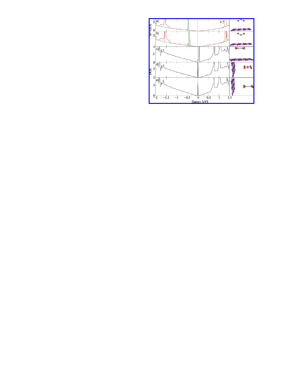
obtained possible adsorption geometries as depicted in Figure
1, right. The corresponding adsorption energies in GGA are
85 meV (a), 67 meV (b), 67 meV (c), 50 meV (d), and 44
meV (e) per molecule, with sheet-adsorbate distances of 3.4-
3.5 Å for the monomer and 3.8-3.9 Å for the dimer. As
usual, LDA yields higher adsorption energies (approximately
169-181 meV for the monomer and 112-280 meV for the
dimer) and favors the adsorbates by 0.5-1 Å nearer to the
sheet. Adsorption near defects can cause higher adsorption
energies, such as, for example, chemisorption of NO
2
at a
vacancy defect yielding 1.8 eV. However, the doping effects
occurring there turn out to be similar to those on perfect
graphene. So we will limit the following discussion to the
latter case.
The spin-polarized DOS of the supercells containing NO
2
,
shown in Figure 1a,b, reveals a strong acceptor level at 0.4
eV below the Dirac point in both adsorption geometries. The
molecular orbitals of NO
2
correspond to flat bands and
manifest themselves as peaks in the DOS. The energies of
these peaks are virtually independent of the adsorbate
orientation. Most important for doping effects is the partially
occupied molecular orbital (POMO) of NO
2
, which is split
by a Hund-like exchange interaction: the spin-up component
of this orbital is approximately 1.5 eV below the Dirac point
and fully occupied, as it is also for the case of free NO
2
molecules. The spin down component of the NO
2
POMO is
unoccupied for free NO
2
, but is 0.4 eV below the Dirac point
in the adsorbed configuration.
25
Hence, it can accept one
electron from graphene in the dilute limit, which corresponds
to the limit of an infinitely large supercell.
By means of band structure calculations, we investigated
the bandwidth and hybridization of the NO
2
acceptor bands
with the graphene bands. It turns out that, in a small region,
less than 1% of the Brillouin zone, where the graphene and
the NO
2
POMO bands come as close as 40 meV, these bands
start mixing significantly. In the entire rest of the Brillouin
zone, the acceptor band is localized almost entirely at the
adsorbate and extends over 5 meV in energy space.
In contrast to the paramagnetic monomer, the dimer, N
2
O
4
,
has no unpaired electrons and is diamagnetic: upon forma-
tion from two monomers, the two POMOs hybridize with
the resulting bonding orbital being the highest occupied
molecular orbital (HOMO). The possibility of doping effects
due to adsorbed dimers has been investigated using the DOS
depicted in Figure 1c-e. Again, the molecular orbitals of
the adsorbates are recognizable as sharp peaks in the
supercell DOS. Similar to NO
2
, band structure calculations
reveal hybridization of the adsorbate and the graphene bands,
where these bands come as close as 40 meV, and an impurity
bandwidth of about 3 meV outside the band crossing region.
One finds that the N
2
O
4
HOMO is in all cases more than 3
eV below the Fermi level and therefore does not give rise
to any doping. However, the lowest unoccupied molecular
orbital (LUMO) is always quite near to the Dirac point, i.e.,
between 1 and 66 meV above it.
26
Those initially empty N
2
O
4
LUMOs can be populated by the graphene electrons as a
result of thermal excitations and act consequently as acceptor
levels. Thus both N
2
O
4
and NO
2
give rise to p-type doping
of graphene, with one decisive distinction: the affinity of
the open shell monomer to accept electrons from graphene
Figure 1. Left: Spin-polarized DOS of the graphene supercells
with adsorbed NO
2
(a,b) and DOS of graphene with N
2
O
4
(c-e),
in various adsorption geometries. The energy of the Dirac points
is defined as E
D
) 0. In the case of NO
2
, the Fermi level E
f
of the
supercell is below the Dirac point, directly at the energy of the
spin down POMO, whereas, for N
2
O
4
, E
f
is directly at the Dirac
points. Right: Adsorption geometries obtained with GGA. The
carbon atoms are printed in blue, nitrogen is shown in green, and
oxygen is shown in red.
174
Nano Lett.,
Vol. 8, No. 1, 2008
Downloaded by UNIV MANCHESTER on July 10, 2009
Published on December 18, 2007 on http://pubs.acs.org | doi: 10.1021/nl072364w
is much stronger than that of the dimer. Note that, despite
the DOS at the Fermi level being high, neither the dimer
nor the monomer are Jahn-Teller active, as there is no orbital
degeneracy.
Our theoretical considerations made so far imply the
following experimentally checkable features: First, there will
be two types of dopants when graphene is exposed to NO
2
s
the monomer and the dimersgiving rise to acceptor levels
far below and rather close to the Dirac point, respectively.
Furthermore, we find both acceptor states almost entirely
localized at the adsorbate molecules and similarly weakly
hybridized with the graphene p
z
bands. Therefore electrons
in both acceptor states should exhibit a similar electron
mobility, which should be much less than the mobility of
the electrons in the graphene bands.
These predictions will be examined experimentally in the
following part of this letter by combining electric field effect
and Hall measurements at different adsorbate concentrations.
To this end, we prepared Hall bar devices with Ti/Au (5
nm/40 nm) contacts from monolayer graphene flakes
18
on
heavily doped oxidized (300 nm SiO
2
) silicon substrate. As
prepared, our samples were unintentionally p-doped, likely
caused by water on the graphene surface. This unintentional
doping was removed by annealing in vacuum for 2 h at 410
K.
1
Then the samples were exposed to NO
2
strongly diluted
in nitrogen (100 ppm of NO
2
) for 60 s at room temperature.
After the exposure, the chamber was evacuated, and the
samples were annealed in a number of annealing cycles while
being constantly kept under vacuum. During each annealing
cycle our, devices were heated up to 410 K, kept at that
temperature for some time, allowing for desorption of some
NO
2
/N
2
O
4
(thus reducing the doping level slightly), and then
cooled to room temperature at which longitudinal R
xx
and
Hall R
xy
resistances were measured at B ) 1 T as a function
of the gate voltage V
G
using a standard low-frequency lock-
in technique. This procedure allowed us to vary the level of
doping gradually in the range from 3
× 10
12
cm
-2
down to
practically pristine state with doping as low as 10
11
cm
-2
by
controlling the time spent at 410 K (varied from 2 min for
the very first cycle up to 16 h for the last cycle, when the
undoped state was reached). At T ) 300 K, the level of
doping achieved after each of the annealing cycles was stable
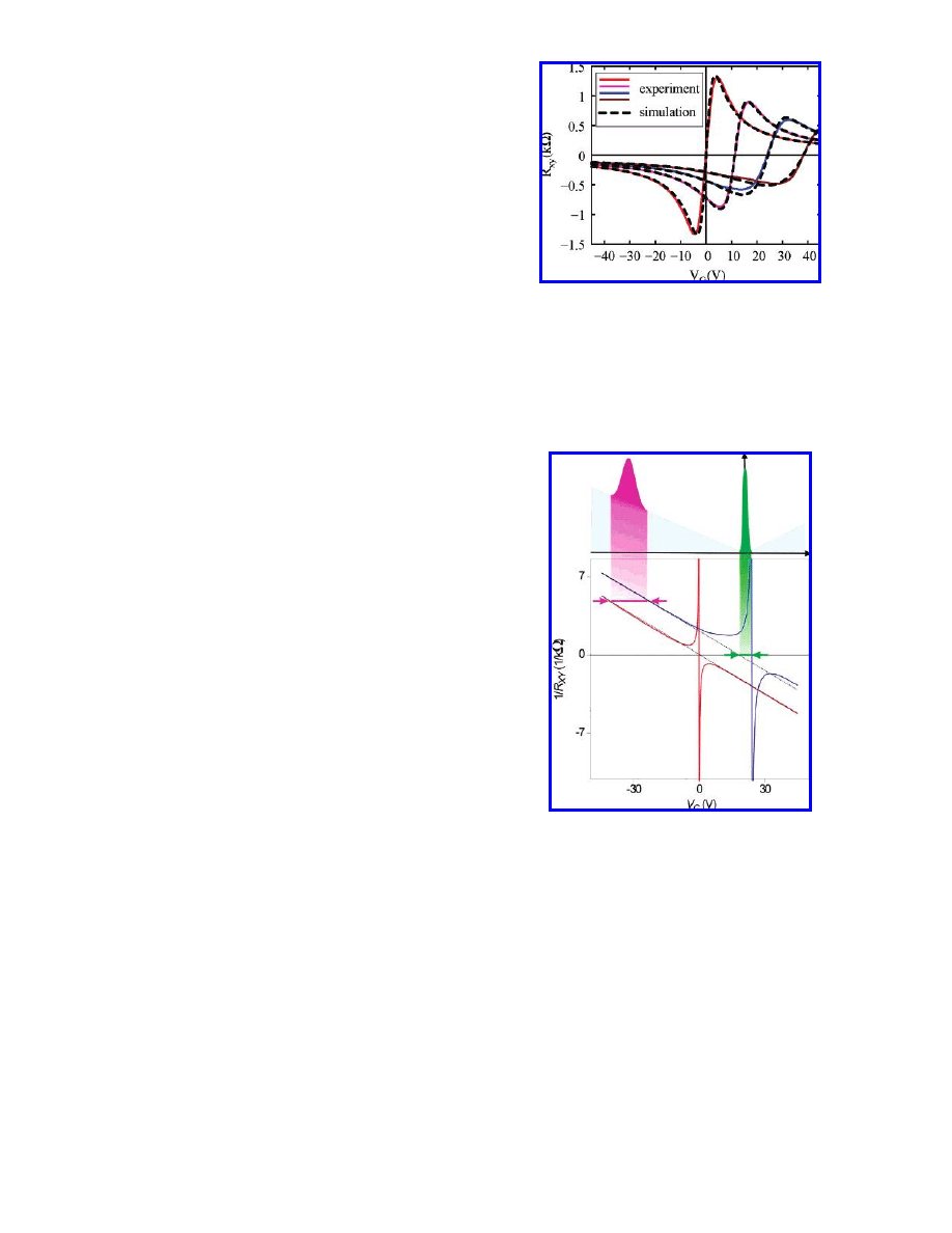
with the precision of a few percent. Figure 2 presents R
xy
as
a function of the gate voltage for a sample annealed in 16
cycles (though only three measurements
27
taken in the 4th,
7th, and 13th cycles, plus the curve for the pristine state are
presented for clarity).
These R
xy
versus V
G
measurements exhibit two character-
istic features. First, the curves move toward higher positive
gate voltages with increasing NO
2
/N
2
O
4
doping. Second, the
transition region, where R
xy
depends linearly on the gate
voltage (corresponding to the presence of both types of
carriers), becomes wider, and, simultaneously, the maximum
R
xy
achieved becomes lower for a higher amount of NO
2
/
N
2
O
4
on the graphene sample. This is clear evidence of the
two distinct acceptor levels, as will be explained in the
following.
Consider 1/R
xy
as shown in Figure 3. The deep acceptor
level causes a solid shift at all V
G
, while the acceptor level
close to the Dirac point gives rise to an additional shift of
the electron branch (straight line at negative 1/R
xy
). The curve
for doped graphene (blue curve) exhibits these two shifts
with respect to the red curve, which corresponds to undoped
graphene. The NO
2
-acceptor level shifts the entire doped
curve to the right, whereas the additional shift of the electron
branch reflects the presence of the N
2
O
4
impurity level near
Figure 2. The Hall resistance R
xy
as a function of the gate voltage
V
G
for a graphene sample with different levels of NO
2
/N
2
O
4
doping.
The solid lines are the experimental results, with the brown curve
corresponding to the highest concentration of adsorbates, and the
red curve corresponding to almost zero doping. The dashed lines
are the simulations. They are fitted to the experimental curves by
adjusting the dopant concentrations c
1
and c
2
for each curve (see
text). The simulation close to the red curve corresponds to undoped
graphene, c
1
) c
2
) 0.
Figure 3. 1/R
xy
for pristine (red curve) and doped (blue curve)
graphene samples. Upper panel: the DOS of doped graphene
(corresponds to the blue curve), with gray depicting the DOS for
pure graphene, the magenta peak representing the DOS for NO
2
,
and the green peak representing N
2
O
4
. Shifting of the blue curve
with respect to the undoped one (red) suggests the presence of the
low-laying NO
2
peak, and the fact that the electron branch for blue
curve is shifted with respect to the hole branch indicates the
presence of the N
2
O
4
peak.
Nano Lett.,
Vol. 8, No. 1, 2008
175
Downloaded by UNIV MANCHESTER on July 10, 2009
Published on December 18, 2007 on http://pubs.acs.org | doi: 10.1021/nl072364w
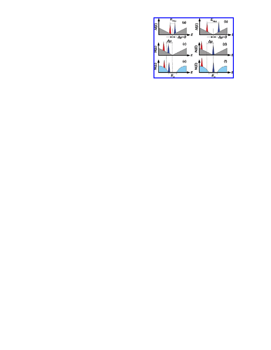
the Dirac point. The latter additional shift in 1/R
xy
displays
as broadening of the transition region near the charge
neutrality point in the R
xy
curves, as discussed above. We
would like to stress that similar behavior can be seen in the
R
xx
curves, where the peak broadens and its position shifts
toward higher positive gate voltages. However, here we
would like to concentrate on R
xy
as the most suggestive
measurements.
To make the analysis more quantitative, we present a
simple model, which is based on the presence of four types
of carriers: electrons and holes in graphene as well as
electrons in the NO
2
and N
2
O
4
acceptor states. Electrons and
holes in graphene have approximately the same, rather high
mobility of about 5000 cm
2
/ Vs.
1
Our DFT calculations
predict the acceptor bands to both be flat with a similar
bandwidth, and a similar, weak hybridization with the
graphene bands is found. Thus, we expect the mobility
µ of
electrons in the impurity states to be much smaller than the
mobility of the electrons in the graphene bands. Expressing
the impurity-state electron mobility
µ in units of the graphene
electron mobility, the Hall resistance is given by
19
R
xy
)
(B(
µ
2
c + n - p)/e(
µc + n + p)
2
), where n (p) is the density
of electrons (holes) in graphene, and c is the density of
electrons in the impurity states. As the gate voltage V
G
)
Rσ is directly related to the total charge density of the sample
σ ) e(c + n - p), where the prefactor R is determined by
substrate properties as described in ref 1, we can simulate
the Hall resistance as a function of V
G
.
To this end, we adjust the global fit parameter R to the
slope of the
|1/R
xy
| curves. Once the impurity-state electron
mobility
µ and the impurity DOS N
imp
are specified, R
xy
and
V
G
are functions of the chemical potential, since n, p, and c
are determined by the graphene DOS and N
imp
, respectively,
via the Fermi distribution function. It turns out that, for
reasonable agreement of all 17 experimental curves (four of
them presented in Figure 2) with the simulations,
µ
≈ 0.1 is
required and N
imp
(E) has to be peaked around two distinct
energies, E
1
e -300 meV and E
2
≈ -40 meV. Taking in
particular N
imp
(E) ) c
1
δ(E - E
1
) + c
2
δ(E - E
2
),
28
we
simulate the R
xy
versus V
G
measurements with three global
fit parameters R,
µ, and E
2
and two curve specific fit
parameters, c
1
and c
2
. E
1
e -300 meV corresponds to our
DFT estimation of E
1
≈ -400 meV. The good agreement
of simulations and experiment (see Figure 2) confirms the
presence of two distinct impurity levels due to the NO
2
and
N
2
O
4
as predicted by DFT. The coefficients c
1
and c
2
are
the measures of the density of electronic states due to the
NO
2
and N
2
O
4
adsorbates, respectively. From the fitting of
the simulations to the experimental curves we obtain c
1
)
1.7, 1.1, and 0.6
× 10
12
cm
-2
and c
2
) 1.3, 0.9, and 0.3 ×
10
12
cm
-2
for the brown, blue, and magenta curve in Figure
2, respectively, corresponding to 3000-10 000 molecules on
a device of 0.75
µm
× 0.75 µm in size.
The deep acceptor level at E
1
e -300 meV due to NO
2
is always fully occupied under our experimental conditions.
This full occupancy corresponds to the transfer of one
electron from graphene sheets to NO
2
per adsorbate molecule,
as observed in ref 3. The occupancy of the NO
2
acceptor
orbital is basically independent of temperature, which is very
different from normal semiconductors, where the acceptor
states are inside the gap and populated as a result of thermal
excitation. Therefore, graphene electronic devices could be
operated at arbitrarily low temperatures, in contrast to usual
semiconductor devices.
Above, we elaborated on the strong difference between
NO
2
and N
2
O
4
adsorbates regarding the impurity level
energies and the doping strength. We would like to argue
that this is a manifestation of a general difference between
the doping by paramagnetic and diamagnetic adsorbates. The
latter type of impurities act generally as rather weak dopants
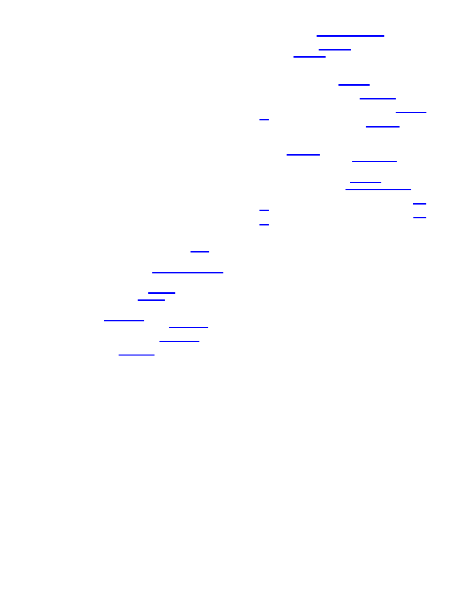
or do not give rise to any doping at all (Figure 4, right
column), whereas the paramagnetic impurities cause strong
doping (Figure 4, left column): closed shell molecules are
chemically rather inert and exhibit HOMO/LUMO gaps
typically on the order of E
HLc
≈ 5-10 eV;
20
for doping by
diamagnetic adsorbates, a mismatch of the molecular and
the graphene chemical potential in the same order of
magnitude or cluster formation is required. For open-shell
systems, the situation is the opposite: as one orbital is only
partially populated, occupied and unoccupied states are only
separated by Hund exchange on the order of E
HLo
≈ 1 eV.
Thus, any open-shell molecule will give rise to doping as
long as the chemical potential mismatch
∆µ between the
adsorbate and graphene exceeds half the Hund exchange
splitting, i.e.,
∆µ J 0.5 eV (see Figure 4). This displays a
close relation between graphene’s DOS and the fact that this
material can be easily doped by many adsorbates. As there
is no gap in the spectrum, a small mismatch in the chemical
Figure 4. Doping dependence on chemical potential mismatch
∆µ,
HOMO/LUMO splitting E
HL
, and the host’s DOS. The left (right)
column corresponds to paramagnetic (nonmagnetic) adsorbates.
(E
HLo
, E
HLc
, see text.) The combined DOS, N(E), (before
equilibration of the adsorbate’s and host’s chemical potentials) is
shown for graphene (a-d) and a semiconductor with a gap E
G
(e,f)
as host material. (a,b)
∆µ ) 0. The adsorbate’s HOMO (red) and
LUMO (blue) are well inside the valence and the conduction bands
of the host, respectively, resulting in no doping (also for a
semiconductor with a gap, not shown here for brevity). (c) A small
mismatch in the chemical potential
∆µ > (1/2)E
HLo
leads to strong
doping in the case of a paramagnetic molecule (NO
2
) on graphene.
(d) A much larger mismatch is required
∆µ > (1/2)E
HLc
to produce
acceptor levels in the case of a paramagnetic molecule (N
2
O
4
) on
graphene. (e,f) The mismatch in chemical potential
|∆µ| > (1/2)(E
HL
+ E
G
), which is required to produce doping in the case of a
semiconductor with a gap is much larger than in the case of
graphene: (e) corresponds to weak doping and (f) to no doping.
176
Nano Lett.,
Vol. 8, No. 1, 2008
Downloaded by UNIV MANCHESTER on July 10, 2009
Published on December 18, 2007 on http://pubs.acs.org | doi: 10.1021/nl072364w
potential can be sufficient to provide an active donor or
acceptor level (see Figure 4). The introduction of a gap in
conventional semiconductors means that the chemical po-
tential mismatch has to exceed half the value of the gap in
order to achieve any doping. Therefore, graphene gas sensors
will, in general, be more sensitive than those built from usual
semiconductors.
Flat bands near the Fermi level are an origin of ferro-
magnetism and many related electronic instabilities. NO
2
molecules adsorbed on graphene create and control the
occupancy of flat impurity bands near the Dirac point as
well as they can lead to exchange scattering. This warrants
future attention, as it can result in strongly spin-polarized
impurity states
21
and lead to a possible pathway
22
to high-
temperature magnetic order in graphene.
Acknowledgment. This work was supported by SFB 668
(Germany) and FOM (The Netherlands). KSN and AKG are
grateful to the Royal Society and EPSRC (UK). SVM and
EEV acknowledge RFBR and the “Quantum Macro Physics”
program (Russia).
References
(1) Novoselov, K. S.; Geim, A. K.; Morozov, S. V.; Jiang, D.; Zhang,
Y.; Dubonos, S. V.; Grigorieva, I. V.; Firsov, A. A. Science 2004,
306, 666-669.
(2) Novoselov, K. S.; Jiang, D.; Schedin, F.; Booth, T. J.; Khotkevich,
V. V.; Morozov, S. V.; Geim, A. K. Proc. Natl. Acad. Sci. U.S.A.
2005, 102, 10451-10453.
(3) Schedin, F.; Geim, A. K.; Morozov, S. V.; Hill, E. W.; Blake, P.;
Katsnelson, M. I.; Novoselov, K. S. Nat. Mater. 2007, 6, 652-655.
(4) Geim, A. K.; Novoselov, K. S. Nat. Mater. 2007, 6, 183-191.
(5) Kong, J.; Franklin, N. R.; Zhou, C. W.; Chapline, M. G.; Peng, S.;
Cho, K. J.; Dai, H. J. 2000, 287, 622-625.
(6) Peng, S.; Cho, K. Nanotechnology 2000, 11, 57-60.
(7) Chang, H.; Lee, J. D.; Lee, S. M.; Lee, Y. H. Appl. Phys. Lett. 2001,
79, 3863-3865.
(8) Zhao, J.; Buldum, A.; Han, J.; Lu, J. P. Nanotechnology 2002, 13,
195-200.
(9) Meijer, E. J.; Sprik, M. J. Chem. Phys. 1996, 105, 8684-8689.
(10) Kresse, G.; Hafner, J. J. Phys.: Condens. Matter 1994, 6, 8245-
8257.
(11) Kresse, G.; Joubert, D. Phys. ReV. B 1999, 59, 1758-1775.
(12) Blo¨chl, P. E. Phys. ReV. B 1994, 50, 17953-17979.
(13) Perdew, J. P. Electronic Structure of Solids ’91; Akademie Verlag:
Berlin, 1991.
(14) Perdew, J. P.; Chevary, J. A.; Vosko, S. H.; Jackson, K. A.; Pederson,
M. R.; Singh, D. J.; Fiolhais, C. Phys. ReV. B 1992, 46, 6671-6687.
(15) Santucci, S.; Picozzi, S.; Gregorio, F. D.; Lozzi, L.; Cantalini, C.;
Valentini, L.; Kenny, J. M.; Delley, B. J. Chem. Phys. 2003, 119,
10904-10910.
(16) Sjovall, P.; So, S. K.; Kasemo, B.; Franchy, R.; Ho, W. Chem. Phys.
Lett. 1990, 172, 125-130.
(17) Moreh, R.; Finkelstein, Y.; Shechter, H. Phys. ReV. B 1996, 53,
16006-16012.
(18) Graphene Industries Home Page. www.grapheneindustries.com
(accessed September 2007).
(19) Kim, J. S. J. Appl. Phys. 1999, 86, 3187-3194.
(20) Zhan, C.-G.; Nichols, J.; Dixon, D. J. Phys. Chem. A 2003, 107,
4184-4195.
(21) Wehling, T. O.; Balatsky, A. V.; Katsnelson, M. I.; Lichtenstein, A.
I.; Scharnberg, K.; Wiesendanger, R. Phys. ReV. B 2007, 75, 125425.
(22) Edwards, D. M.; Katsnelson, M. I. J. Phys.: Condens. Matter 2006,
18, 7209-7225.
(23) Kim, W.; Javey, A.; Vermesh, O.; Wang, Q.; Li, Y.; Dai, H. Nano
Lett. 2003, 3, 193-198.
(24) Bradley, K.; Cumings, J.; Star, A.; Gabriel, J.-C. P.; Gru¨ner, G. Nano
Lett. 2003, 3, 639-641.
(25) The energies of the POMO spin up and down orbitals relative to the
Dirac points predicted by LDA are -0.5eV and -1.4eV, respectively,
i.e., in almost quantitative agreement with the GGA results.
(26) LDA locates these LUMOs between 2 meV and 210 meV above the
Dirac point.
(27) Hysteretic behavior (in V
G
) was observed when visiting large gate
voltages (above 40 V) For the sweep rates used in our experiments
(15 V/min), the typical hysteresis was 1.5 V; however, it could be
as high as 5 V if the time spent at high voltages was too long. Such
hysteresis has been discussed in refs 23 and 24, but the exact cause
of this effect is beyond the scope of this paper. Here, we always
present the data obtained during sweeps from negative to positive
voltages (-45 V f +45 V), and we always made sure that the time
spent at -45 V was kept at a minimum.
(28) The broadness of the impurity levels does not strongly influence the
simulations.
NL072364W
Nano Lett.,
Vol. 8, No. 1, 2008
177
Downloaded by UNIV MANCHESTER on July 10, 2009
Published on December 18, 2007 on http://pubs.acs.org | doi: 10.1021/nl072364w
Wyszukiwarka
Podobne podstrony:
12 Nano Lett 8 2442 2446 2008id Nieznany (2)
16 Nano Lett 8 17041708 2008id Nieznany (2)
173 177 207cc pol ed02 2008
15 Nature Nano 3 210 215 2008id Nieznany (2)
finanse publiczne Podatki (173 okna)
W 21 Alkohole
21 02 2014 Wykład 1 Sala
21 Fundamnety przyklady z praktyki
BO I WYKLAD 01 3 2011 02 21
w 1 komunikacja 21 11 09 nst
21 25
176 177
więcej podobnych podstron