ConstruCtion
60 • December 2006 • electronics for you
w w w . e f y m a g . c o m
M
ore and more experiments
are now ‘PC-assisted.’ Also
conventional acquisition sys-
tems are very expensive. Since portable
PCs are today common and a USB link
is a better solution than an old ISA bus,
here we present an oscilloscope using
USB port of the PC that operates at up
to 10 kHz with ±16V input voltage. It
has much more improved features than
the PC-based oscilloscope and LED
scope for audio servicing published in
EFY Dec. 2002 and Electronics Projects
Vol. 8, respectively. The oscilloscope
uses IC PIC18F2550 from Microchip
as the main controller, which makes
the oscilloscope compact as there is no
need of additional power supply for
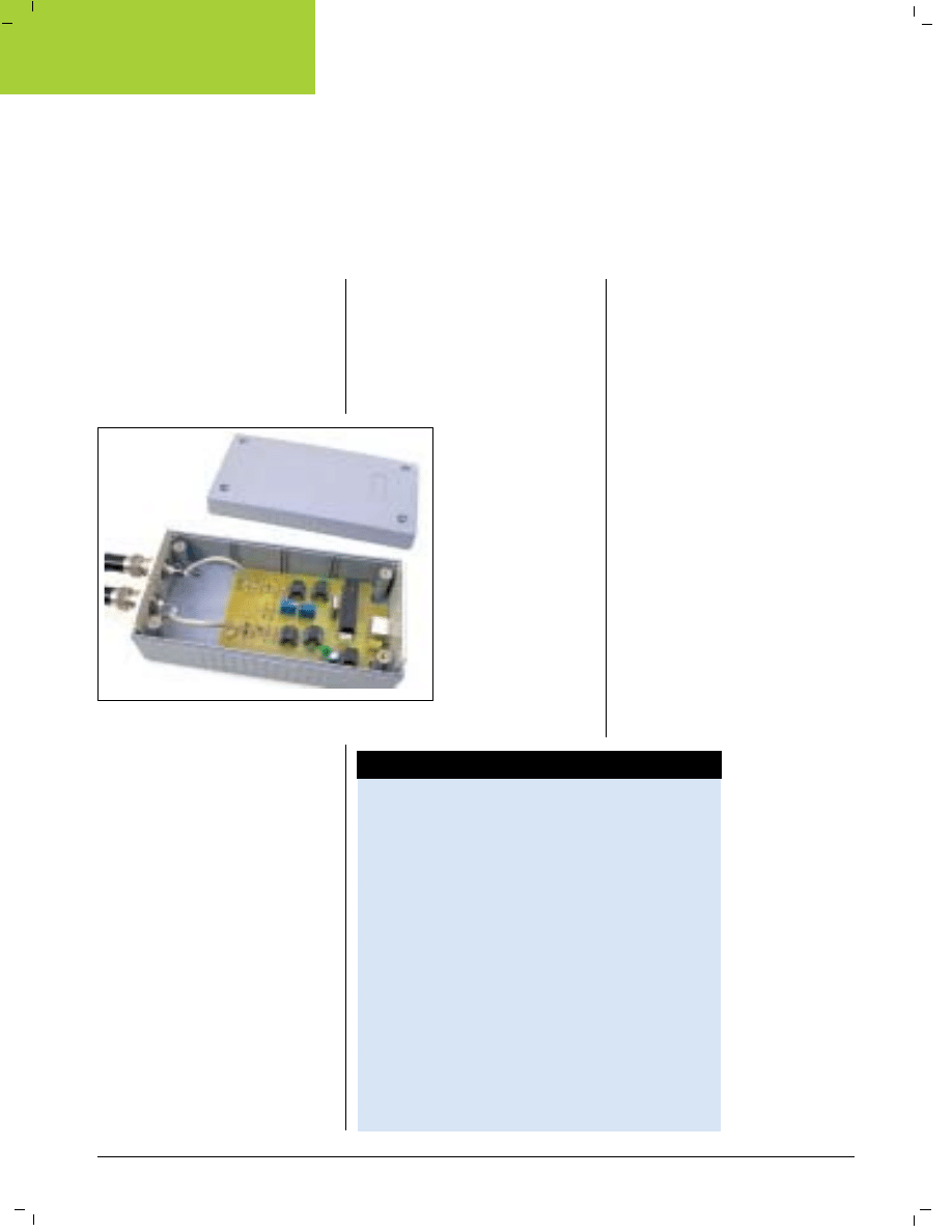
the entire circuit board. The prototype
of the circuit along with the enclosure
is shown above.
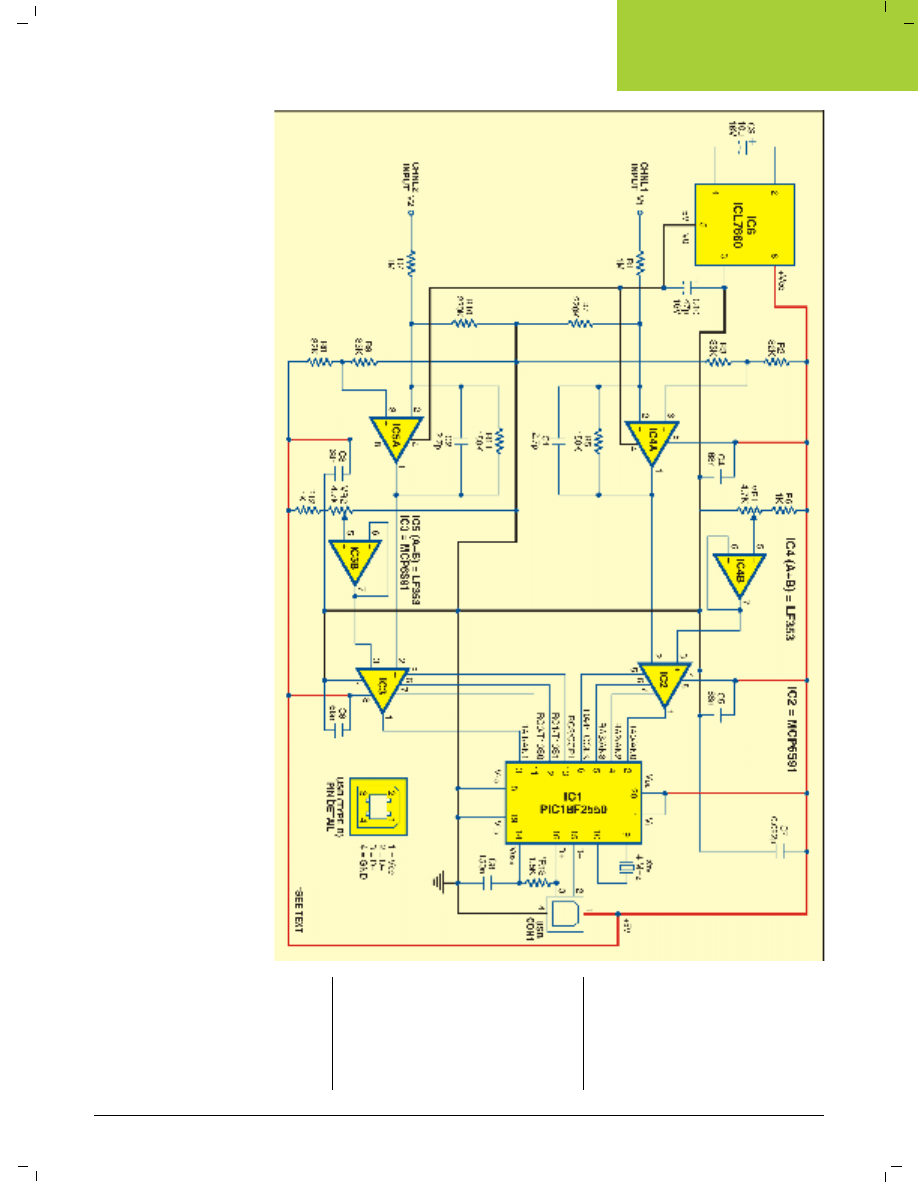
Circuit description
At the heart of this oscilloscope is
USB2.0-compliant microcontroller
PIC18F2550 from Microchip. You
can also use PIC18F2445 in place of
PIC18F2550. Specifications of this mi-
its pins 5, 6 and 7.
The MCP6S91 amplifier is designed
with CMOS input devices. It is de-
signed to not exhibit phase inversion
when the input pins exceed the supply
voltages. The maximum voltage that
can be applied to the input pin is –0.3V
(V
SS
) to +0.3V (V
DD
). Input voltages that
exceed this absolute maximum rating
can cause excessive current into or out
of the input pins. Current beyond ±2
mA can cause reliability problems. Ap-
plications that exceed this rating must
be externally limited with a resistor to
the input pin.
Vref (pin 3), which is an analogue
input, should be at a voltage between
V
SS
and V
DD
. The voltage at this pin
shifts the output voltage. The SPI
interface inputs are chip-select (CS),
serial input (SI) and serial clock (SCK).
These are Schmitt-triggered, CMOS
logic inputs.
The only disadvantage is that these
amplifiers accept only positive signals.
That’s why voltage-shifting ampli-
fiers LF353 (IC4A
and IC5A) are used,
one each for each
channel input (see
Fig. 1). The LF353
is a JFET input op-
erational amplifier
with an internally
compensated input
offset voltage. The
JFET input device
provides wide band-
width, low input
bias currents and
offset currents. This
voltage-shifting am-
plifier results in a
high input imped-
ance and an attenu-
ation factor of 1:4.5.
A ±16V input signal
is then shifted to the
crocontroller are given here in the box.
This microcontroller has a USB2.0-com-
pliant transceiver and a CPU running
up to 12 MIPS.
Fig. 1 shows the circuit of the
two-channel PC-based oscilloscope.
MCP6S91 from Microchip Technology
is an analogue programmable gain am-
plifier that is well suited
to driving analogue-to-
digital converters (ADCs)
and an analogue input to
a PIC microcontroller.
Two MCP6S91 pro-
grammable gain ampli-
fiers (IC2 and IC3) make
it possible to choose the
input ranges for each of
the two channels, by se-
lecting a gain from 1:1 to
32:1. The amplifiers are
small, cheap and easy to
use. A simple three-wire
serial peripheral inter-
face (SPI) allows the PIC
to control them through
Gerard SamblanCat
two-Channel PC-
baSed oSCilloSCoPe
Author’s prototype
Features of PIC18F2550
Programming
1. Up to 32 kB of flash memory, 2kB RAM and 256-byte EEPROM
2. Extended instruction set (optimised for ‘C’ compiler)
3. 8x8 single-cycle multiplier
4. Single-supply serial programming and easy debugging
USB transceiver
1. USB1.1 and 2.0 from 1.5 MB/s to 12 MB/s
2. Isochronous, bulk and interrupt transfer modes
3. 1 kB of access RAM usable with 32 endpoints (64 bytes each)
Multiple oscillator and power modes
1. From internal 31 kHz to external 48 MHz with PLL
2. Possible software switching between ‘run,’ ‘idle’ and sleep
modes. In sleep mode, current is down to 0.1 µA.
3. Wide operating voltage range (2.0V to 5.5V). Useful for battery
operations.
Complete set of classical peripherals
1. Several input/output (I/O) ports, four timers with capture/
compares
2. Synchronous and asynchronous enhanced modules
3. Streaming parallel port
4. 10-bit ADC module with up to 13-channel multiplexer.
ConstruCtion
electronics for you • December 2006 • 61
w w w . e f y m a g . c o m
0-5V range when the pro-
grammed gain is 1:1.
Two halves of the
LF353 (IC4B and IC5B) are
used as voltage follow-
ers to provide a low-im-
pedance shifting voltage
(Vref) to the program-
mable amplifiers. This
voltage must be precisely
adjusted with two 4.7-kilo-
ohm presets to measure
precisely 2.5V level on
the inputs of IC2 and IC3
when the input signals are
grounded.
Because LF353 op-
amps need a symmetrical
supply voltage, a small
DC-DC voltage converter
ICL7660 (IC6) is used
to feed –5V to LF353.
With its small 8-pin DIP
package, it needs only
two polarised capacitors.
ICL7660 can be replaced
with a MAX1044. The
MAX1044 and ICL7660
are monolithic, CMOS
switched-capacitor volt-
age converters that invert,
double, divide or multiply
a positive input voltage.
These are pin compatible
with the industry-stan-
dard LTC1044.
overview of the
universal serial
bus
The specifications of the
USB can be found on web-
site ‘www.usb.org.’ One
of its major advantages
is the ability to drive 5V,
100mA devices.
All the data is trans-
mitted on the D+/D- sym-
metrical pins using a vari-
able bit rate. The position
of a resistor (R13) on D+
or D- allows you to choose between
the full-speed (12 Mbps) and low-
speed modes (1.5 Mbps). Note that the
PIC18F2550/2455 devices have built-in
pull-up resistors designed to meet the
requirements of low-speed and full-
speed USB. The UPUEN bit (UCFG=4)
enables the internal pull-ups. In this
project, R13 is not used. External pull-
up may also be used. The VUSB pin
may be used to pull up D+ or D-. The
pull-up resistor must be 1.5 kilo-ohms
(±5%) as required by the USB specifica-
tions.
You can also ‘hot-plug’ a new de-
vice. When this is done, the host PC
starts an enumeration process to iden-
tify the device. The device sends the in-
formation to the PC by way of different
‘descriptors.’ Each descriptor contains
Fig.
1:
Two-channel
PC
-based
oscilloscope
circuit
ConstruCtion
62 • December 2006 • electronics for you
w w w . e f y m a g . c o m
a specific kind of information about
the device (vendor ID, serial number,
format and type of data transmitted).
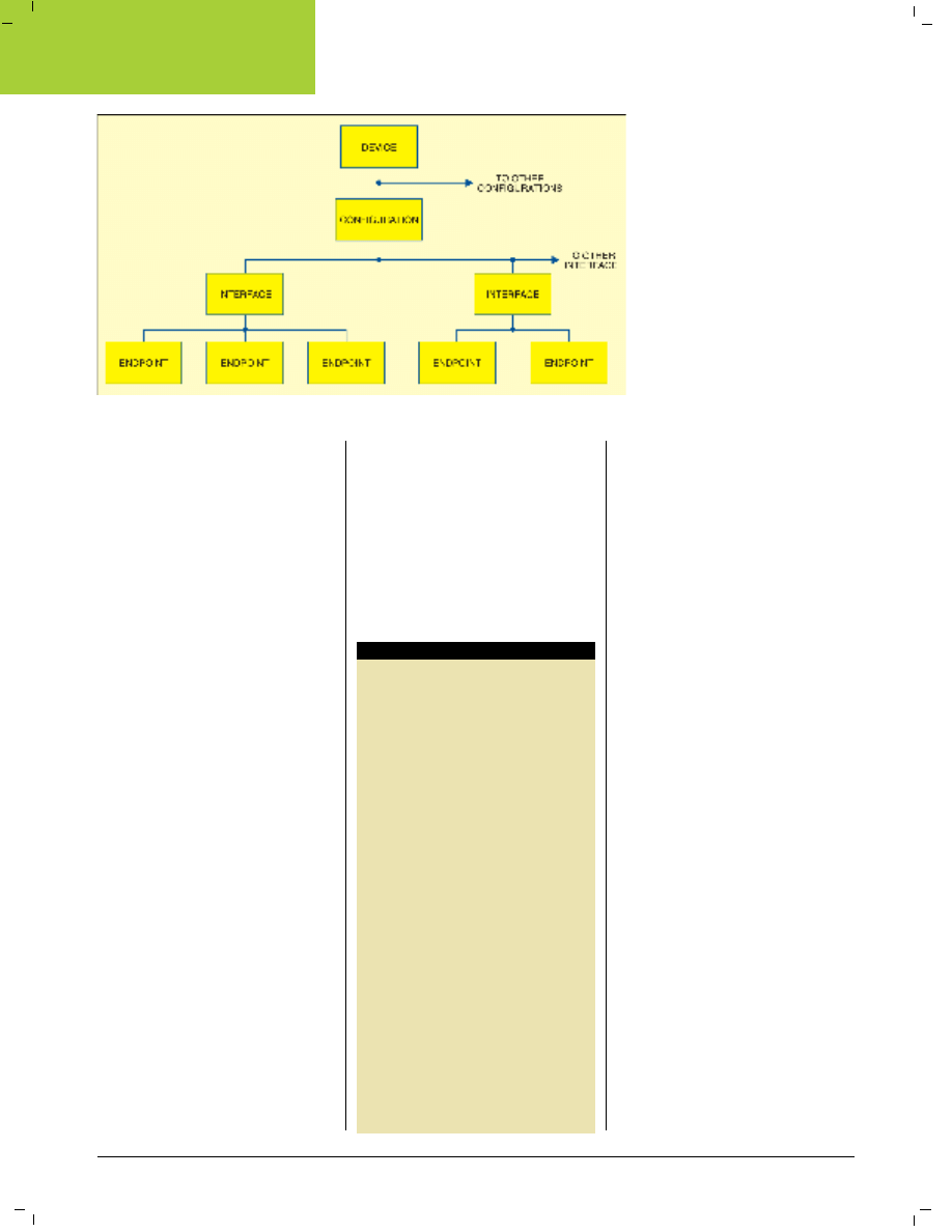
You can see in Fig. 2 that each
device is structured in a layered frame-
work of descriptors. The first layer con-
taining the configuration descriptors
describes the power mode.
Each configuration may have dif-
ferent interfaces and each interface
may have different endpoints. An
interface can use several endpoints
and an endpoint can be ‘IN’ (data from
device to the host) or ‘OUT’ (from host
to the device). With such an opened
structure, it’s important to carefully
design the descriptors.
A 64-byte buffer is allocated to
each of the 32 possible endpoints. Here
only one is used and the more possible
amount of RAM buffer is then reallo-
cated to store the measured values.
the PiC software
The program for the microcontroller
is written in ‘C’ language. MPLAB
7.31 along with MPLAB_C18 is used
as the software tool for develop-
ment. The software tools can be
downloaded for free from website
‘www.microchip.com.’
Based on Microchip’s application
notes, the program for the chip is cen-
tered on a main loop continually poll-
ing the USB transceiver state. This loop
never stops and each USB operation is
done in one pass. All operations are
initiated by the host (the PC), which
sends a 16-byte command.
The first command byte determines
the chip actions. The four possible ac-
tions are:
1. Command 80h: Clears the EE-
PROM calibration memory
2. Command 81h: Receives param-
eters, and stores the gain-error com-
pensation for the two channels.
3. Command 83h: Initiates a zero
calibration sequence of the two chan-
Fig. 2: Layered framework of a USB device
nels. The two inputs have to be
grounded.
4. Command 85h: Initiates mea-
surement of the input signals.
The PIC software consists of
eight ‘C’ program source files, 14
header files and a linker file all un-
der ‘aquis.mcp’ project. The main
‘C’ program source files (‘main.c’
and ‘user.c’) are given at the end of
this article. The rest of the program
files are included in the EFY-CD.
Programming the chip. Program-
ming the PIC18F2455/2550 is easy
with an ICD2 module or PICSTART
Plus development board along with
MPLAB software. But many serial
programmers for PIC16F84 are not
compatible here. While using the
PICSTART Plus development board,
you can copy the hex file into the
MPLAB IDE using ‘import’ command
from ‘file’ menu bar. Select the device
as ‘PIC18F2550’ and configure the bits
as per this device from ‘config’ menu.
Installation of the USB driver. 1. If
everything is fine, plug the oscilloscope
with a USB cable to your PC (running
Windows 98SE or higher version). A
“new hardware detected–USB2-Min-
iOscilloscope” dialogue box must im-
mediately appear on the screen.
2. Now you can start the driver in-
stallation process. The driver has been
included in the EFY-CD. The goal is
to select a good driver (mchpusb.inf)
by choosing the ‘specific location’ op-
tion. Don’t let Windows take a generic
driver by default.
3. When you are done with
installation, go to ‘device manager’
and check whether ‘USB2-MiniOscillo-
scope’ is under ‘other device’ in ‘view
devices by type’ option. Otherwise,
repeat Steps 1 and 2.
User interface program and op-
erations. A user-interface software
written in Visual Basic 6, called ‘Os-
cilloPIC,’ is included in the EFY-CD.
Run the set up program from the
‘Setup_files’ folder included in the
EFY-CD. This will automatically install
the ‘OscilloPIC’ user-interface pro-
gram. Alternatively, you can open the
‘Source_VB6’ folder, compile and run
the ‘Synchropic’ program using Visual
Basic 6. Now run the ‘OscilloPIC.’ The
Parts List
Semiconductors:
IC1
- PIC18F2550 microcon-
troller
IC2, IC3
- MCP6S91 program-
mable gain amplifier
IC4(A, B),
IC5(A, B)
- LF353 dual operational
amplifier
IC6
- ICL7660 switched-ca-
pacitor voltage convert-
ers
Resistors (all ¼-watt, ±5% carbon):
R1, R7
- 1-mega-ohm
R2, R8
- 82-kilo-ohm
R3, R9
- 33-kilo-ohm
R4, R10
- 220-kilo-ohm
R5, R11
- 150-kilo-ohm
R6, R12
- 1-kilo-ohm
Capacitors:
C1, C2
- 2.7pF ceramic
C3, C4,
C5, C6
- 68nF ceramic
C7
- 0.022µF polyester
C8
- 150nF ceramic
C9
- 10µF, 16V electrolytic
C10
- 47µF, 16V electrolytic
Miscellaneous:
X1
- 4MHz crystal oscillator
CON1
- USB socket (type-B) for
PCB
ConstruCtion
electronics for you • December 2006 • 63
w w w . e f y m a g . c o m
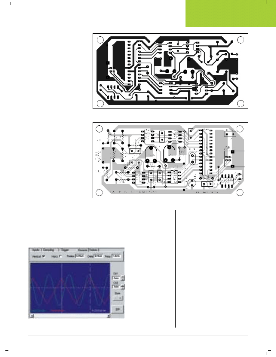
application program looks like a
small digital oscilloscope as shown
in the screenshot below.
Various settings for operations
are given in the following menu
bars:
1. Inputs: Selects the active
channels
2. Sampling: Sets time-base and
number of samples
3. Trigger: Sets the triggering
condition
4. Cursors: Selects horizontal or
vertical cursor positions
5. Num: Shows numerical
sampled values, with an export
command (text file format)
6. Config: Configures gain and
offset errors
Calibration is to be done as
described below before reading
the output signals on the monitor
screen by clicking ‘channels cali-
bration’ under ‘config’ menu bar.
Feed the input waveforms (say,
sine, rectangular, sawtooth, etc)
from the source. Click ‘go’ but-
ton. The output waveform will be
displayed on the monitor screen.
Channel-1 and channel-2 output
waveforms can be differentiated by
green and red lines, respectively.
By default, the time base is 200 µs
per division and amplitude is 4V
per division. You can set these param-
eters as per your requirements.
Test and calibration. The first
step is to adjust the zero offset error.
Connect the two analogue inputs to
the ground level and tune the two 4.7-
kilo-ohm presets until pin 2 of both
MCP6S21 is at 2.5V. A more precise
tuning can be achieved through ‘Oscil-
loPIC’ software. Choose the smallest
calibration value at ±0.5V for both the
inputs.
The ‘zero calibration’
command tells the PIC
to start its own internal
compensation for all cali-
brations. Don’t forget to
connect the inputs to the
ground while calibrat-
ing.
The second parameter
to check is the gain error.
By clicking the ‘gain cali-
bration’ command, it’s
possible to specify a small
correction factor. This
can be done after several
measurements. You have
to know the actual levels
Screenshot: Oscilloscopic program output screen along with typical
sine and triangular waveforms
Fig. 3: An actual-size, single-side PCB layout of the two-channel PC-based USB oscilloscope
Fig. 4: Component layout for the PCB
and the measured levels (with the cur-
sors) for the two channels. The gain er-
ror is less than 0.1 per cent. The number
of samples can be set between ‘10’ and
‘500.’ The minimum sampling rate is
5 µs for one channel and 10 µs for two
channels.
Construction
An actual-size, single-side PCB layout
for the two-channel PC-based USB os-
cilloscope circuit is shown in Fig. 3 and
its component layout in Fig. 4. Since
the circuit is compact, the construction
is easy. It is advised to use IC bases for
mounting IC2 through IC6 on the PCB
for easy troubleshooting. The USB con-
nector (CON1) must be firmly soldered
and fixed on the board. It is located on
the extreme right of the board (refer
Fig. 4).
Two BNC connectors can be used
for the input signals for channels ‘1’

ConstruCtion
64 • December 2006 • electronics for you
w w w . e f y m a g . c o m
/**********************************************************
* FileName: main.c
* Dependencies: See INCLUDES section below
/** I N C L U D E S ************************************/
#include “p18f2550.h”
#include “typedefs.h” // Required
#include “usb.h” // Required
#include “io_cfg.h” // Required
#include “user.h” // Modifiable
/** V A R I A B L E S ***********************************/
#pragma udata
extern unsigned char voie1[256];
extern unsigned char voie2[256];
extern unsigned char voiesH1[64],voiesH2[64];
extern char ordre, timeout;
/** P R I V A T E P R O T O T Y P E S ****************/
static void InitializeSystem(void);
void USBTasks(void);
void timer_isr(void);
/** V E C T O R M A P P I N G *********************/
extern void _startup (void); // See c018i.c in
//your C18 compiler dir
#pragma code _RESET_INTERRUPT_VECTOR =
0x000800
void _reset (void) {
_asm goto _startup
_endasm
}
#pragma code
#pragma code low_vector = 0x18
void low_interrupt (void) {
_asm
goto timer_isr
_endasm
}
#pragma code
#pragma interruptlow timer_isr
//Fixe une periode de 1 seconde pour le time-out
//aquisition
maIn.C
void timer_isr(void) {
//Reset l’it du timer 1
INTCONbits.TMR0IF=0;
TMR0H= 256-183;
TMR0L= 0;
timeout++; // incremente le compteur time-out !!
}
/*#pragma code _LOW_INTERRUPT_VECTOR =
0x000818
void low_ISR (void) {
;
}*/
/** D E C L A R A T I O N S **************************/
#pragma code
/******************************************************
****
* Function: void main(void)
* PreCondition: None
* Input: None
* Output: None
* Side Effects: None
* Overview: Main program entry point.
* Note: None
**********************************************************
*******************/
void main(void) {
InitializeSystem();
ordre=0;
while(1) {
USBTasks(); // USB Tasks
ProcessIO(); // See user\user.c & .h
}//end while
}//end main
/*********************************************************
*********************
* Function: static void InitializeSystem(void)
* PreCondition: None
* Input: None
* Output: None
* Side Effects: None
* Overview: InitializeSystem is a centralize ini-
/**********************************************************
* FileName: user.c
* Processor: PIC18
********************************************************
************/
/** I N C L U D E S ************************************/
#include “p18f2550.h”
#include “typedefs.h”
#include “usb.h”
#include “io_cfg.h” // I/O pin mapping
#include “user.h”
/** V A R I A B L E S **********************************/
#pragma udata
DATA_PACKET databuff;
//Caracteristiques de l’acquisition
unsigned char t_basethh, t_baseth, t_basetl;
unsigned char t_seuilh, t_seuill;
unsigned int t_nbpts;
//Boucle de dechargement vers le bus Usb
int send1_pts, send2_pts, s_shift;
int send1H_pts, send2H_pts, sendoffs;
user.C
//Compteur et pointeur des buffers de voies
unsigned char acqcyc, timeout;
unsigned char ordre;
unsigned char vH1, vH2, nptsH, nptsL;
unsigned char testH, testL;
unsigned char tt1, tt2, tt3;
unsigned char savFSR1L, savFSR1H,savFSR2L,
savFSR2H;
//--- Reservation de 640 octets pour la voie 1 -----
// de 0x100 a 0x37F
#pragma udata voieA = 0x100
unsigned char voie1A[256];
#pragma udata voieB = 0x200
unsigned char voie1B[256];
#pragma udata voiesMSB = 0x300
unsigned char voiesH1[128];
//--- La voie 2 est UsbRam de 0x500 a 0x77f -----
/** P R I V A T E P R O T O T Y P E S ***************/
void CopyData(unsigned int addr);
unsigned char RdEEPROM(unsigned char ad);
void WrEEPROM(unsigned char ad, unsigned char
dat);
/** D E C L A R A T I O N S **************************/
#pragma code
/***********************************************************
* Initialisation des ports, timer1, Adcon
*
********************************************************
**********/
void UserInit(void) {
//!!! NE PAS RALENTIR AVANT L’ENUM USB !!!
//Reglage ADC voie AN0 ok
ADCON0 = 0x01;
/ /
adc on
ADCON1 = 0b00001101; // no ref , AN0-1
ADCON2 = 0b10001100; // 2.Tad Fosc/4
PORTA = 0b11110011;
TRISA = 0b11100011; //cde MCP6S ch0
TRISB = 0xff;
PORTC = 0b11111100;
TRISC = 0b11111000; //cde MCP6S ch1
send1_pts = send2_pts = 0;
send1H_pts = send2H_pts = 0;
sendoffs=0;
}
and ‘2,’ respectively. The connectors
can be fixed on the front panel of the
enclosure.
The performance of the oscilloscope
can be improved by changing the PIC
and its ADC with a faster model.
AD9238 (20 MS/s) is a good choice.
This fast, parallel ADC converter could
be used with a powerful DSP PIC. A
PIC18Fx455 could be used for its USB
link. An auto-zero-level calibration
system could be a good idea. This can
be done with an analogue switch on all
input signals.
EFY Note. All the relevant software
of this article have been included in
this month’s EFY CD.
tialization routine.
* All required USB initialization routines
are called from
* here.
* User application initialization routine
should also be
* called from here.
**********************************************************
*******************/
static void InitializeSystem(void) {
ADCON1 |= 0x0F; // Default all pins to digital
#if defined(USE_USB_BUS_SENSE_IO)
tris_usb_bus_sense = INPUT_PIN; // See io_cfg.
h
#endif
#if defined(USE_SELF_POWER_SENSE_IO)
tris_self_power = INPUT_PIN;
#endif
UserInit(); // See user.c & .h
mInitializeUSBDriver(); // See usbdrv.h
}//end InitializeSystem
/*********************************************************
*********************
* Function: void USBTasks(void)
* PreCondition: InitializeSystem has been called.
* Input: None
* Output: None
* Side Effects: None
* Overview: Service loop for USB tasks.
**********************************************************
*******************/
void USBTasks(void) {
/* Servicing Hardware */
USBCheckBusStatus(); // Must use
polling method
if(UCFGbits.UTEYE!=1)
USBDriverService(); // Interrupt or
polling method
}// end USBTasks
/** EOF main.c ****************************************/

ConstruCtion
electronics for you • December 2006 • 65
w w w . e f y m a g . c o m
/***********************************************************
* Function: Lecture data eeprom
**************************************************************/
unsigned char RdEEPROM(unsigned char ad) {
EEADR=ad;
_asm
bcf
EECON1,7,0
// clear EEPGD
bcf
EECON1,6,0
// clear CFGS
bsf
EECON1,0,0
// set RD
_endasm
return(EEDATA);
}
/***********************************************************
* Proc: Ecriture data eeprom
********************************************************
***********/
void WrEEPROM(unsigned char ad, unsigned char
dat) {
EEADR=ad;
EEDATA=dat;
_asm
bcf
EECON1,7,0
// clear EEPGD
bcf
EECON1,6,0
// clear CFGS
bsf
EECON1,2,0
// set WREN
movlw 0x55
movwf EECON2,0
movlw 0xAA
movwf EECON2,0
bsf
EECON1,1,0
// set WR
_endasm
while (EECON1bits.WR!=0) { ; }
_asm
bcf
EECON1,2,0
// raz WREN
_endasm
}
/***********************************************************
* Function: void SetGain0(char)
* Overview:
Change le gain program-
mable ampli voie0.
***********************************************************/
void SetGain0(unsigned char gain) {
unsigned char nn, q;
CS_CH0=0;
//Envoie cde ecriture registre gain (SPI 0.0)
nn=0b01000000;
for (q=0;q<8;q++) {
if (nn&128) SI_CH0=1; else SI_CH0=0;
SCK_CH0=1;
nn<<=1;
SCK_CH0=0;
}
//Envoie le gain (SPI 0.0)
nn=gain;
for (q=0;q<8;q++) {
if (nn&128) SI_CH0=1; else SI_CH0=0;
SCK_CH0=1;
nn<<=1;
SCK_CH0=0;
}
CS_CH0=1;
}
/***********************************************************
* Function: void SetGain1(char)
* Overview:
Change le gain program-
mable ampli voie1.
*****************************************************************/
void SetGain1(unsigned char gain) {
unsigned char nn, q;
CS_CH1=0;
//Envoie cde ecriture registre gain (SPI 0.0)
nn=0b01000000;
for (q=0;q<8;q++) {
if (nn&128) SI_CH1=1; else SI_CH1=0;
SCK_CH1=1;
nn<<=1;
SCK_CH1=0;
}
//Envoie le gain (SPI 0.0)
nn=gain;
for (q=0;q<8;q++) {
if (nn&128) SI_CH1=1; else SI_CH1=0;
SCK_CH1=1;
nn<<=1;
SCK_CH1=0;
}
CS_CH1=1;
}
/************************************************************
* Function: CopyData (int)
* Overview: Recopie un bloc de 64 octets vers
databuff.
* avant envoie sur le bus USB.
***************************************************************/
void CopyData(unsigned int addr) {
_asm
decf
FSR1L,1,0 //!!! adr sur 8
bits
decf
FSR1L,1,0
movf
INDF1,0,0 // recup le
Msb
movwf
FSR0H,0
decf
FSR1L,1,0
movf
INDF1,0,0 // recup le Lsb
movwf
FSR0L,0
//Sauve FSR2
movf
FSR2H,0,0
movwf
vH2,1
movf
FSR2L,0,0
movwf
tt2,1
movlw
databuff
// adr sur 16
bits
movwf
FSR2L,0
movlw
0
// !!!!
movwf
FSR2H,0
movlw
64
movwf
vH1,1
//Boucle de copie
copydo:
movf
POSTINC0,0,0
movwf
POSTINC2,0
decfsz
vH1,1,1
bra
copydo
incf
FSR1L,1,0
incf
FSR1L,1,0
incf
FSR1L,1,0
//Restitue FSR2
movf
vH2,0,1
movwf
FSR2H,0
movf
tt2,0,1
movwf
FSR2L,0
_endasm
}
/***********************************************************
* Function: Mesure sur voies sur les ADC
**************************************************************/
unsigned int doADC(unsigned char voie) {
if (voie==0) ADCON0=5; else ADCON0=1;
_asm
//lance mesure voie
bsf
ADCON0,1,0
// lance aquis
waitvn:
btfsc
ADCON0,1,0
bra
waitvn
_endasm
return(ADRES);
}
void doADC0(void) {
ADCON0=5;
_asm
//lance mesure voie 0
bsf
ADCON0,1,0
// lance aquis
waitv0:
btfsc
ADCON0,1,0
bra
waitv0
_endasm
}
void doADC1(void) {
ADCON0=1;
_asm
//lance la mesure voie 1
bsf
ADCON0,1,0
// lance aquis
waitv1:
btfsc
ADCON0,1,0
bra
waitv1
_endasm
}
/***********************************************************
* Function: void ProcessIO(void)
* Overview: This function is a place holder for
other user routines.
* It is a mixture of both USB and non-USB
tasks.
***********************************************************/
void ProcessIO(void) {
unsigned char ordrelen, pt;
unsigned int level;
unsigned long int sum32;
// User Application USB tasks
if((usb_device_state < CONFIGURED_
STATE)||(UCONbits.SUSPND==1)) return;
ordrelen=(USBGenRead((byte*)&databuff,16));
//Verifie que le prefixe est recu
if (ordrelen!=0) ordre=databuff._byte[0];
//====================================
// RECEPTION COMMANDE RAZ
//ETALONNAGE
//====================================
if (ordre==0x80) {
//Raz premier eeprom location
pt=0xff;
WrEEPROM(2,pt); // msb zero shift = ff
WrEEPROM(4,pt); // ‘’
‘’
//Lance l’emission des offs en accusé de recep-
tion
sendoffs=64;
ordre=0;
} //fin si ordre=80
//====================================
// RECEPTION COEFFICIENTS DE GAIN
//====================================
if (ordre==0x81) {
//Sauve les coeff de gain Voie 1
pt=databuff._byte[1];
WrEEPROM(9,pt);
//Voie 2
pt=databuff._byte[2];
WrEEPROM(10,pt);
//Lance l’emission des offs en accusé de recep-
tion
sendoffs=64;
ordre=0;
} //fin si ordre=81
//====================================
// RECEPTION COMMANDE REGLAGE DU
//ZERO
//====================================
if (ordre==0x83) {
//Met les calibres +/-16v
SetGain0(0);
SetGain1(0);
sum32=0;
//Moyenne de 256 acquisitions
for (level=0;level<0x100;level++) {
sum32+=doADC(0);
for (tt1=0;tt1<64;tt1++) { ; }
}
//Sauve moyenne Voie0+/-16v en eeprom 1-2
pt=sum32>>8;
WrEEPROM(1,pt);
pt=sum32>>16;
WrEEPROM(2,pt);
//Moyenne de 256 acquisitions
sum32=0;
for (level=0;level<0x100;level++) {
sum32+=doADC(1);
for (tt1=0;tt1<64;tt1++) { ; }
}
//Sauve moyenne Voie1+/-16v en eeprom 3-4

ConstruCtion
66 • December 2006 • electronics for you
w w w . e f y m a g . c o m
pt=sum32>>8;
WrEEPROM(3,pt);
pt=sum32>>16;
WrEEPROM(4,pt);
//===================================
//Met les calibres +/-1v
SetGain0(6);
SetGain1(6);
sum32=0;
//Moyenne de 256 acquisitions - voie 0
for (level=0;level<0x100;level++) {
sum32+=doADC(0);
for (tt1=0;tt1<64;tt1++) { ; } }
//Sauve moyenne Voie0+/-1v en eeprom
pt=sum32>>8;
WrEEPROM(5,pt);
pt=sum32>>16;
WrEEPROM(6,pt);
//Moyenne de 256 acquisitions - voie 1
sum32=0;
for (level=0;level<0x100;level++) {
sum32+=doADC(1);
for (tt1=0;tt1<64;tt1++) { ; } }
//Stocke ecarts en eeprom
pt=sum32>>8;
WrEEPROM(7,pt);
pt=sum32>>16;
WrEEPROM(8,pt);
//Lance l’emission des offs en accusé de recep-
tion
sendoffs=64;
ordre=0;
} //fin si ordre=83
//====================================
// RECEPTION COMMANDE ACQUISITION
//====================================
if (ordre==0x85) {
//Met les calibres demandés
SetGain0(databuff._byte[8]);
SetGain1(databuff._byte[9]);
//Prend le mode et seuil de declenchement
t_seuilh=databuff._byte[1];
t_seuill=databuff._byte[2];
//Prend la base de temps sur 24 bits
t_basethh=databuff._byte[3];
t_baseth=databuff._byte[4];
t_basetl=databuff._byte[5];
//Prend le nombre de points
nptsH = databuff._byte[6];
nptsL = databuff._byte[7];
t_nbpts= nptsL + 256*nptsH;
//--------- Vidage de la memoire courbes ---------
_asm
movlw
1
// Voie 1 - 100h/37fh
movwf
FSR0H,0
clrf FSR0L,0
raz1: clrf INDF0,0
decfsz FSR0L,1,0
bra
raz1
incf FSR0H,1,0
clrf FSR0L,0
raz2: clrf INDF0,0
decfsz FSR0L,1,0
bra
raz2
incf FSR0H,1,0
movlw
127
// met les msb à 512
movwf
FSR0L,0
raz3: movlw
0xAA
movwf
INDF0,0
decfsz FSR0L,1,0
bra
raz3
movwf
INDF0,0
movlw
5
// Voie 2 - 500h/77fh
movwf
FSR0H,0
clrf FSR0L,0
raz4: clrf INDF0,0
decfsz FSR0L,1,0
bra
raz4
incf FSR0H,1,0
clrf FSR0L,0
raz5: clrf INDF0,0
decfsz FSR0L,1,0
bra
raz5
incf FSR0H,1,0
movlw
127
// met les msb a 512
movwf
FSR0L,0
raz6: movlw
0xAA
movwf
INDF0,0
decfsz FSR0L,1,0
bra
raz6
movwf
INDF0,0
//------------ Prepare Acquisition ----------------
incf nptsH,1,1 // compense les decfsz...
movf FSR1H,0,0 // sauve FSR1
movwf
savFSR1H,1 // pour apres
aquis
movf FSR1L,0,0 //
movwf
savFSR1L,1 //
movf FSR2H,0,0 // sauve FSR2
movwf
savFSR2H,1 // pour apres
aquis
movf FSR2L,0,0 //
movwf
savFSR2L,1 //
movlw
0x1
movwf
FSR0H,0
movlw
0x5
movwf
FSR2H,0
clrf FSR0L,0
// fsr0 ptr de lsb
voie 0
clrf FSR2L,0
// fsr2 ptr de lsb
voie 1
movlw
0x3
movwf
FSR1H,0
clrf FSR1L,0
// fsr1 ptr de
msb v0&v1
movlw
4
// raz paquet de poids forts
movwf
acqcyc,1
clrf vH1,1
clrf vH2,1
_endasm
//-------- Conditions declenchement ---------
// t_seuilh - b7 =1 : synchro
//
b6 =0 : voie0, =1:voie1
//
b5 =1 : montant, =0:descen-
dant
//
b4 =1 : voie1 active
//
b3 =1 : voie0 active
// t_seuilh 1:0 +seuill = niveau vu par ADC direct.
if (t_seuilh & 0x80) {
//Si synchro sur un seuil alors
level = t_seuill+0x100*(t_seuilh&0x3);
T0CON=0b10010110;
TMR0H= 256-183;
TMR0L= 0;
INTCON=0b10100000;
timeout=0;
//Si synchro sur VOIE 1
if (t_seuilh & 0x40) {
//Sync sur front montant
if (t_seuilh & 0x20) {
doADC0();
while (ADRES>=level)
{ doADC0(); if (timeout==15) break; }
while (ADRES<level)
{ doADC0(); if (timeout==15) break; } }
else {
//Sync sur front descendant
doADC0();
while (ADRES<level)
{ doADC0(); if (timeout==15) break; }
while (ADRES>=level)
{ doADC0(); if (timeout==15) break; } }
} // fin si voie1
//Si synchro sur VOIE 2
else {
if (t_seuilh & 0x20) {
doADC1();
while (ADRES>=level)
{ doADC1(); if (timeout==15) break; }
while (ADRES<level)
{ doADC1(); if (timeout==15) break; } }
else {
//Sync sur front descendant
doADC1();
while (ADRES<level)
{ doADC1(); if (timeout==15) break; }
while (ADRES>=level)
{ doADC1(); if (timeout==15) break; } }
} // fin si voie2
INTCON=0;
}
//====================================
// AQUISITION DE LA VOIE 0 SEULE - MINI
//MUM 5 uS
//====================================
if ((t_seuilh & 0x18)==0x08) {
_asm
movlw
0x01
movwf
ADCON0,0
bsf
ADCON0,1,0
// lance aquis
nop
nop
loopv0:
movff
ADRESL,POSTINC0
// stocke lsb voie 0
bcf STATUS,0,0 // prend les deux bits
rlcf vH1,1,1
rlcf vH1,0,1
// decale de 2 et OR
iorwf ADRESH,0,0
movwf
vH1,1
//Test si cycle de Msb
decfsz acqcyc,1,1 // decr ctr
bra
stoh0
//Stocke les 4*2 bits finis
movf vH1,0,1
movwf POSTINC1,0 // FSR1 pointeur MSB
clrf vH1,1
// raz next msb
movlw
4
movwf acqcyc,1 // raz acqcyc
bra
dosui0
stoh0:
movlw
1 // tempo compens
pti1: decfsz WREG,1,0
//
bra
pti1
//
nop
//
//Relance next aquisition
dosui0: bsf
ADCON0,1,0
// lance aquis
//Tempo d’une periode d’ech basehh->33mS
movff t_basethh, tt3
movff t_baseth, tt2
movff t_basetl, tt1
tpo1:
decfsz
tt1,1,1
bra
tpo1
decfsz tt2,1,1
bra
tpo1
decfsz tt3,1,1
bra
tpo1
//Compte le nombre de points sur 16 bits
decfsz nptsL,1,1
bra
loopv0
decfsz nptsH,1,1
bra
loopv0
_endasm
}
//====================================
// AQUISITION DE LA VOIE 1 SEULE - MINI
//MUM 5 uS
//====================================
if ((t_seuilh & 0x18)==0x10) {
_asm

ConstruCtion
electronics for you • December 2006 • 67
w w w . e f y m a g . c o m
movlw
0x7
movwf FSR1H,0
// msb voie2 en
0x7xx
movlw
0x05
movwf
ADCON0,0
bsf
ADCON0,1,0 // lance aquis
nop
loopv1:
movff
ADRESL,POSTINC2
// sto lsb voie1 (fsr2)
bcf STATUS,0,0
// prend les
deux bits
rlcf vH1,1,1
rlcf vH1,0,1
// decale de 2 et OR
iorwf ADRESH,0,0
movwf
vH1,1
//Test si cycle de Msb
decfsz acqcyc,1,1 // decr ctr
bra
stoh1
//Stocke les 4*2 bits finis
movf vH1,0,1
movwf
POSTINC1,0
// FSR1 pointeur MSB
clrf vH1,1
// raz next msb
movlw
4
movwf
acqcyc,1
// raz acqcyc
bra
dosui1
stoh1:
movlw
1 // tempo compens
pti2: decfsz WREG,1,0
//
bra
pti2
//
nop
//
//Relance next aquisition
dosui1: bsf ADCON0,1,0 // lance aquis
//Tempo d’une periode d’ech basehh->33mS
movff t_basethh, tt3
movff t_baseth, tt2
movff t_basetl, tt1
tpo2:
decfsz
tt1,1,1
bra
tpo2
decfsz tt2,1,1
bra
tpo2
decfsz tt3,1,1
bra
tpo2
//Compte le nombre de points sur 16 bits
decfsz nptsL,1,1
bra
loopv1
decfsz nptsH,1,1
bra
loopv1
_endasm
}
//====================================
// AQUISITION DES DEUX VOIES - MINIMUM
//10 uS
//====================================
if ((t_seuilh & 0x18)==0x18) {
_asm
// Acquisition de la Voie 0
loopaq:
movlw
0x05
movwf
ADCON0,0
bsf
ADCON0,1,0
// lance aquis
nop
nop
movff ADRESL,POSTINC0 // stocke lsb voie 1
bcf STATUS,0,0
// prend les
deux bits
rlcf vH1,1,1
rlcf vH1,0,1
// decale de 2 et OR
iorwf ADRESH,0,0
movwf
vH1,1
//Test si cycle de Msb
decfsz acqcyc,0,1 // (decr sans modifier)
bra
stoh2
//Stocke les 4*2 bits finis
movf vH1,0,1
movwf
INDF1,0
clrf vH1,1
// raz new msb
bra
do_v2
stoh2:
movlw
1 // tempo compens
ptit1:
decfsz
WREG,1,0 //
bra
ptit1
//
nop
//
//-------- Acquisition sur Voie 1 (AN1) ---------
do_v2:
movlw
0x01
movwf
ADCON0,0
bsf
ADCON0,1,0
nop
nop
nop
movff ADRESL,POSTINC2 // stocke lsb voie 2
bcf STATUS,0,0 // prend 2 Msbs
rlcf vH2,1,1
rlcf vH2,0,1
iorwf ADRESH,0,0
movwf
vH2,1
//Test si cycle de Msb
decfsz acqcyc,1,1
bra
stoh3
//Stocke les 4*2 bits finis
movlw
0x4
addwf FSR1H,1,0 // passe en 0x7..
movf vH2,0,1
movwf
POSTINC1,0
movlw
0x4
subwf FSR1H,1,0 // repasse en 0x3..
clrf vH2,1
// raz next Msb
movlw
4
movwf
acqcyc,1
// raz acqcyc
bra
do_sui
stoh3:
movlw
3 // tempo compens
ptit2:
decfsz
WREG,1,0 //
bra
ptit2
//
nop
//
//Tempo d’une periode d’ech basehh->33mS
do_sui: movff
t_basethh, tt3
movff t_baseth, tt2
movff t_basetl, tt1
tp1: decfsz tt1,1,1
bra
tp1
decfsz tt2,1,1
bra
tp1
decfsz tt3,1,1
bra
tp1
//Compte le nombre de points sur 16 bits
decfsz nptsL,1,1
bra
loopaq
decfsz nptsH,1,1
bra
loopaq
_endasm
}
//====================================
//Remet contexte fsr apres aquisitions
_asm
movf savFSR1H,0,1
// remet FSR1
movwf
FSR1H,0
movf savFSR1L,0,1
movwf
FSR1L,0
movf savFSR2H,0,1
// remet FSR2
movwf
FSR2H,0
movf savFSR2L,0,1
movwf
FSR2L,0
_endasm
ordre=0;
//Lance la retransmission
send1_pts = t_nbpts;
s_shift = 0x100;
send1H_pts = send2_pts =send2H_pts = send-
offs=0;
} //fin if ordre=85
/******** ENVOI DE LA VOIE 1 *****************/
if (send1_pts>0) {
//Envoi le premier groupe de 64oc de la Voie 1
CopyData(s_shift);
s_shift+=64;
send1_pts-=64;
//Voit si envoie les 128 Msb max
if (send1_pts<=0) {
send1H_pts=128; // lance les 128 msb
s_shift=0x300; }
while(mUSBGenTxIsBusy()) { }
USBGenWrite((byte*)&databuff,USBGEN_EP_
SIZE);
}
else {
/****** ENVOI DE LA VOIE 1 - POIDS FORTS ******/
if (send1H_pts>0) {
//Envoi le premier groupe des 128 msb de la
Voie 1
CopyData(s_shift);
s_shift+=64;
send1H_pts-=64;
//Voit si envoie les 128 Msb max
if (send1H_pts<=0) {
send2_pts= t_nbpts; // lance envoi voie 2
s_shift=0x500; }
while(mUSBGenTxIsBusy()) { }
USBGenWrite((byte*)&databuff,USBGEN_EP_
SIZE); }
else {
/************ ENVOI DE LA VOIE 2 *****************/
if (send2_pts>0) {
//Envoi le premier groupe de 64oc de la Voie 1
CopyData(s_shift);
s_shift+=64;
send2_pts-=64;
//Voit si envoie les 128 Msb max
if (send2_pts<=0) {
send2H_pts=128; // lance les 128 msb
s_shift=0x700; }
while(mUSBGenTxIsBusy()) { }
USBGenWrite((byte*)&databuff,USBGEN_EP_
SIZE); }
else {
/******* ENVOI DE LA VOIE 2 - POIDS FORTS *****/
if (send2H_pts>0) {
//Envoi le premier groupe des 128 msb de la
Voie 1
CopyData(s_shift);
s_shift+=64;
send2H_pts-=64;
sendoffs=64;
//Voit si envoi des Offsets
while(mUSBGenTxIsBusy()) { }
USBGenWrite((byte*)&databuff,USBGEN_
EP_SIZE); }
else
/********* ENVOI DES OFFSETS VOIE 0 & 1 *********/
if (sendoffs>0) {
//Envoi le premier groupe offsets à +/-16v
databuff._byte[0]=RdEEPROM(1);
/ /
Lsb voie 0
databuff._byte[1]=RdEEPROM(2);
/ /
Msb
databuff._byte[2]=RdEEPROM(3);
/ /
Lsb voie 1
databuff._byte[3]=RdEEPROM(4);
/ /
msb
//Envoi le second groupe offsets à +/-1v
databuff._byte[4]=RdEEPROM(5);
/ /
Lsb voie 0
databuff._byte[5]=RdEEPROM(6);
/ /
Msb
databuff._byte[6]=RdEEPROM(7);
/ /
Lsb voie 1
databuff._byte[7]=RdEEPROM(8);
/ /
msb
//Calibration des gains sauvés en eeprom
databuff._byte[8]=RdEEPROM(9);
/ /
voie 0
databuff._byte[9]=RdEEPROM(0x0a);
/ /
voie 1
//envoie les octets offset + cal gains
while(mUSBGenTxIsBusy()) { }
USBGenWrite((byte*)&databuff,USBGEN_
EP_SIZE);
sendoffs=0;
}
}
}
}
}//end ProcessIO
/****************************************************/
Wyszukiwarka
Podobne podstrony:
PC Based Automation
Model Based Analysis of Two Fighting Worms
A PIC CONTROLLER FOR GRID CONNECTED PV SYSTEM USING A FPGA BASED INVERTER
Evaluation of Two Host Based Intrusion Prevention Systems
BUDOWA KOMPUTERA PC
Content Based, Task based, and Participatory Approaches
pc 01s084 085
pc 07s084 087
pc 08s020 027
Czę¶ć ogólna PC wykład 2 podmioty
Instrukcja programu PC Suite SonyEricsson
Applying Water Based Interior Finish
problem based learning
Anatomia PC Wydanie VIII
pc 04s044 049
pc 02s076 079
pc 03s038 039
więcej podobnych podstron