F2833x - Architecture
2 - 1
Introduction
The TMS320F2833x Digital Signal Controller is capable of executing six basic operations in a
single instruction cycle, and therefore the architecture of the device must reflect this feature in
some way. Remember this key point when we look into the details of this Digital Signal
Controller (DSC). It will help you to understand the ‘philosophy’ behind the device with its
different hardware units. Doing six basic maths operations is no magic; we will find all the
hardware modules that are required to do so in this chapter.
In this and other modules, we will discuss the following parts of the architecture:
•
Internal bus structure
•
CPU
•
Direct Memory Access Controller
•
Floating-point Arithmetic Unit
•
Fixed-point Hardware Multiplier, Arithmetic-Logic-Unit, Hardware-Shifter
•
Pipeline Processing of Instructions
•
Memory Map
3 - 1
Digital Signal Controller
TMS320F2833x
Texas Instruments Incorporated
European Customer Training Centre
University of Applied Sciences Zwickau
Module 2: Architecture
Architecture

Module Topics
2 - 2
F2833x - Architecture
Module Topics
Architecture ................................................................................................................................................2-1
Introduction .............................................................................................................................................2-1
Module Topics ..........................................................................................................................................2-2
TMS320F2833x Block Diagram .........................................................................................................2-3
Bus System ..........................................................................................................................................2-3
Central Processing Unit (CPU) ............................................................................................................2-4
Fixed-point Math Unit .........................................................................................................................2-5
Floating-point Math Unit .....................................................................................................................2-6
Data Memory Access ...........................................................................................................................2-7
Internal Bus Structure ..........................................................................................................................2-8
Direct Memory Access Controller (DMA) ..........................................................................................2-9
Atomic Arithmetic Logic Unit (ALU) ...............................................................................................2-10
Instruction Pipeline ............................................................................................................................2-11
Memory Map .....................................................................................................................................2-12
Code Security Module .......................................................................................................................2-13
Interrupt Response .............................................................................................................................2-14
Operating Modes ...............................................................................................................................2-15
Reset Behaviour .................................................................................................................................2-16
Summary of TMS320F2833x Architecture .......................................................................................2-17
Module Topics
F2833x - Architecture
2 - 3
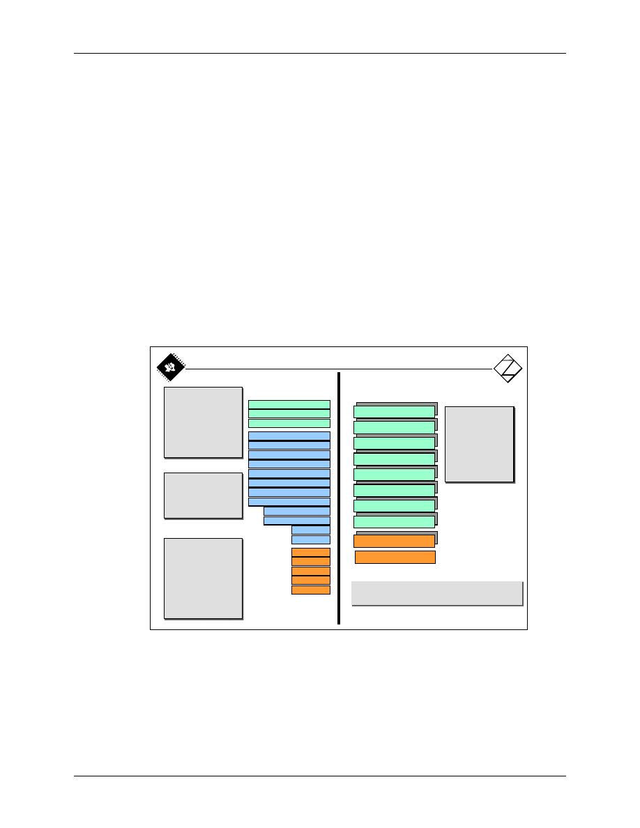
TMS320F2833x Block Diagram
The TMS320F2833x Block Diagram can be divided into the following functional units:
•
Internal and external Bus System
•
Central Processing Unit (CPU)
•
Internal Memory Sections
•
Control Peripherals
•
Communication Channels
•
Direct Memory Access Controller (DMA)
•
Interrupt Management Unit (PIE) and Core Time Unit
•
Real - Time Emulation Interface
2 - 2
A(19-0)
D(31-0)
32x32 bit
Multiplier
Sectored
Flash
Program Bus
Data Bus
RAM
Boot
ROM
32-bit
Auxiliary
Registers
3
32-bit
Timers
Real-Time
JTAG
Emulation
CPU
Register Bus
R-M-W
Atomic
ALU
PIE
Interrupt
Manager
eQEP
12-bit ADC
Watchdog
CAN 2.0B
I2C
SCI
SPI
GPIO
ePWM
eCAP
FPU
McBSP
DMA
6 Ch.
X
IN
TF
DMA Bus
F2833x Block Diagram
Bus System
Since the core of the TMS2833x Microcontroller is a DSP, it must be able to read at least two
operands from memory and transfer them to the central processing unit in a single clock cycle. To
do so, the F2833x features two independent bus systems, called the "Program Bus" and the "Data
Bus". This type of processor technology is called “Harvard-Architecture”. Due to the ability of
the F2833x to read operands not only from data memory but also from program memory, Texas
Instruments calls its technology a “modified Harvard-Architecture”. The “bypass”-arrow in the
bottom left corner of Slide 2-3 indicates this additional feature.
In addition, the F2833x connects all units inside the CPU core to a third bus system, called the
“Register Bus”, allowing a very fast exchange of data between its parallel mathematical units.
Module Topics
2 - 4
F2833x - Architecture
Finally, because the DMA unit is able to operate on certain parts of the hardware units
independently of the CPU, a "Direct Memory Access Bus" has been added for this purpose.
On the left hand side of the slide you will notice a multiplexer block for data (D31-D0) and
address (A19-A0). This is an interface to connect external devices to the F2833x. Please note that
you cannot access the external program bus data and the data bus data simultaneously. Compared
to a single cycle for internal access to two 32-bit operands, it takes at least 2 cycles to do the same
with external memory, not taking into account additional wait cycles for slower external
memories!
Central Processing Unit (CPU)
The F2833x - CPU is able to execute most of the instructions to perform register-to-register oper-
ations and a range of instructions that are commonly used by micro controllers, e.g. byte packing
and unpacking and bit manipulation in a single cycle. The architecture is also supported by po-
werful addressing modes, which allow the compiler as well as the assembly programmer to gen-
erate compact code that almost corresponds one-to-one with the C code.
The F2833x is as efficient in typical math tasks for Digital Signal Processing as it is in the system
control tasks that are typically handled by microcontroller devices. This efficiency removes the
need for a second processor in many systems.
2 - 3
F2833x CPU
32-bit fixed and floating point DSP ; 32 x 32 bit fixed-point MAC
Additional 32 x 32 bit hardware floating point unit
Dual 16 x 16 single-cycle fixed-point MAC (DMAC)
32-/64-bit saturation
Unique real-time debugging capabilities
3
32-bit
Timers
PIE
Interrupt
Manager
32x32 bit
Multiplier
32-bit
Auxiliary
Registers
CPU
Register Bus
R-M-W
Atomic
ALU
FPU
Program Bus
Data Read Bus
Data Write Bus
Real-Time
JTAG
Emulation
Three 32-bit timers can be used for general timing purposes or to generate hardware driven time
periods for real-time operating systems. The Peripheral Interrupt Expansion Manager (PIE)
allows fast interrupt response to the various sources of external and internal signals and events.
The PIE-Manager processes individual interrupt vectors for all sources and reduces the response
time to an external event, called "Interrupt Latency", to an absolute minimum.
Module Topics
F2833x - Architecture
2 - 5
A fixed-point 32-bit by 32-bit hardware multiplier and a 32-bit arithmetic logic unit (ALU) can
be used in parallel to simultaneously execute a multiply and an add operation on fixed-point
numbers. The auxiliary register group is equipped with its own arithmetic unit (ARAU)-also used
in parallel to perform pointer arithmetic. In addition, a hardware floating-point unit (FPU) for
IEEE-754 single point precision numbers allows the direct usage of floating-point numbers from
C or MatLab-code.
The JTAG-interface is a very powerful tool to support real-time data exchange between the DSC
and a host during the debug phase of project development. A special operating mode called
"Real-time Debug" allows variables to be monitored while the code is running in real-time,
without a single clock cycle delay to the control code.
Fixed-point Math Unit
The 32-bit by 32-bit fixed-point “Multiply and Accumulate (MAC)” capabilities of the F2833x
and its internal 64-bit processing capabilities enable this DSC to efficiently handle higher numer-
ical resolution problems based on fixed-point numbers. In control applications, a lot of algorithms
are numerically based on a technique, called "Binary Fractions", sometimes also called "Integer-
Quotient (IQ)"-numbers. The F2833x directly supports this approach. Furthermore, if the sam-
ples and coefficients are stored in a binary number of 16 bits or less, which is quite often possible,
this controller is able to perform two 16-bit by 16-bit multiply and accumulate instructions simul-
taneously. The terminology for such an instruction is “Dual Multiply and Accumulate (DMAC)”.
2 - 4
XT (32) or T/TL
MULTIPLIER
32 x 32 or
Dual 16 x 16
P (32) or PH/PL
AH (16)
F2833x Fixed Point Multiplier and ALU
Data Bus
Data Bus
Program Bus
ALU (32)
32
32
32
32
32
AL (16)
32
32
•
16/32
8/16
Shift R/L (0-16)
ACC (32)
AH.MSB AH.LSB AL.MSB AL.LSB
32
Shift R/L (0-16)
32
Shift R/L (0-16)
32
16
8/16/32
Fixed-point multiplication uses the XT ("eXtended Temp") register to hold the first operand and
multiply it by a second operand, which is loaded from memory. If XT is loaded from a data
memory location and the second operand is fetched from a program memory location, a single-
cycle multiply operation can be performed. The result of a multiplication is shifted into the P
("Product") register or directly into the Accumulator (ACC). Remember, if you multiply a 32-bit
by a 32-bit number, what size is the result? Answer: 64-bits. The F2833x instruction set includes
Module Topics
2 - 6
F2833x - Architecture
two groups of multiply operations to store both 32-bit portions of the result into P and ACC. In
this way, we can say that the registers ACC and P are combined to form a single 64-bit register.
Three hardware shifters can be used in parallel with other hardware units of the CPU. Shifters are
usually used to scale intermediate results in a real-time control loop or just to multiply/divide by
numbers of type 2
n
.
The Arithmetic Logic Unit (ALU) performs all other mathematical operations other than
multiplication. The first operand is always the content of the Accumulator (ACC) or a part of it.
The second operand for an operation is loaded from data memory, from program memory, from
the P register or directly from the multiply unit.
Floating-point Math Unit
To add more flexibility to the device by using single precision floating-point data types in C,
Texas Instruments have added a second hardware multiply unit to the F2833x family. The right
hand side of Slide 2-5 shows all the floating-point registers. The 8 general purpose registers (R0H
to R7H) are supported by a status register (STF) and a repeat block register (RB). The latter is
used to execute a block of machine code without the need for a software loop. Such a technique
allows the pipeline of the CPU to run at faster speeds.
2 - 5
F2833x Floating Point Unit FPU
ACC
P
XT
XAR0
XAR1
XAR2
XAR3
XAR4
XAR5
XAR6
XAR7
PC
RPC
DP
SP
ST0
ST1
IER
IFR
DBGIER
C28 Register Set
R0H
R1H
R2H
R3H
R5H
R6H
R7H
R4H
STF
FPU Register Set
RB
R0H – R7H And STF Are Shadowed For
Fast Context Save And Restore
32-bit
8 FPU Result
Registers
FPU Status
Repeat Block
32-bit
Accumulator
Product
Temporary
8 Auxiliary
22-bit
Program Counter
Return PC
16-bit
Data Page Pointer
Stack Pointer
2 Status
Interrupt Enable
Interrupt Flag
Fixed Point
Floating Point
The left hand part of Slide 2-5 shows the fixed-point register set. It consists of the 3 CPU
registers, Accumulator (ACC), Product (P) and extended temp (XT), 8 general purpose registers
(XAR0…XAR7) and a set of control and status registers, such as "Program Counter" (PC), "Data
Page Pointer"(DP), "Stack Pointer" (SP), "Interrupt Enable" (IER), "Interrupt Flag" (IFR) and
"Debug Interrupt Enable" (DBGIER).
Module Topics
F2833x - Architecture
2 - 7
Data Memory Access
Two basic methods are available to access data memory locations:
•
Direct Addressing Mode
•
Indirect Addressing Mode
2 - 6
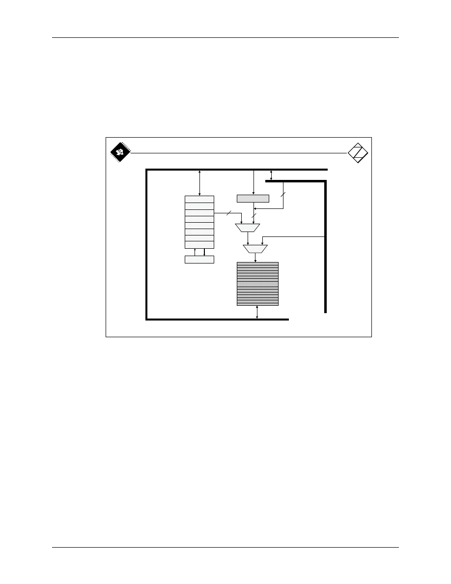
F2833x Pointer, DP and Memory
XAR0
XAR1
XAR2
XAR3
XAR4
XAR5
XAR6
XAR7
ARAU
MUX
Data Memory
MUX
DP (16)
Data Bus
Program Bus
6 LSB
from IR
XARn
→ 32-bits
ARn
→ 16-bits
22
32
Direct addressing mode generates the 22-bit address for a memory access from two sources - a
16-bit register “Data Page (DP)” for the highest 16 bits plus another 6 bits taken from the
instruction. Advantage: Once DP is set, we can access any location of the selected page, in any
order. Disadvantage: If the code needs to access another page, DP must be changed first.
Indirect addressing mode uses one of eight 32-bit XARn registers to hold the 32-bit address of the
operand. Advantage: With the help of the ARAU, pointer arithmetic is available in the same cycle
in which an access to a data memory location is made. Disadvantage: A random access to data
memory needs the pointer register to be setup with a new value.
The auxiliary register arithmetic unit (ARAU) is able to perform pointer manipulations in the
same clock cycle as the access is made to a data memory location. The options for the ARAU are:
post-increment, pre-decrement, index addition and subtraction, stack relative operation, circular
addressing and bit-reverse addressing with additional options.
Module Topics
2 - 8
F2833x - Architecture
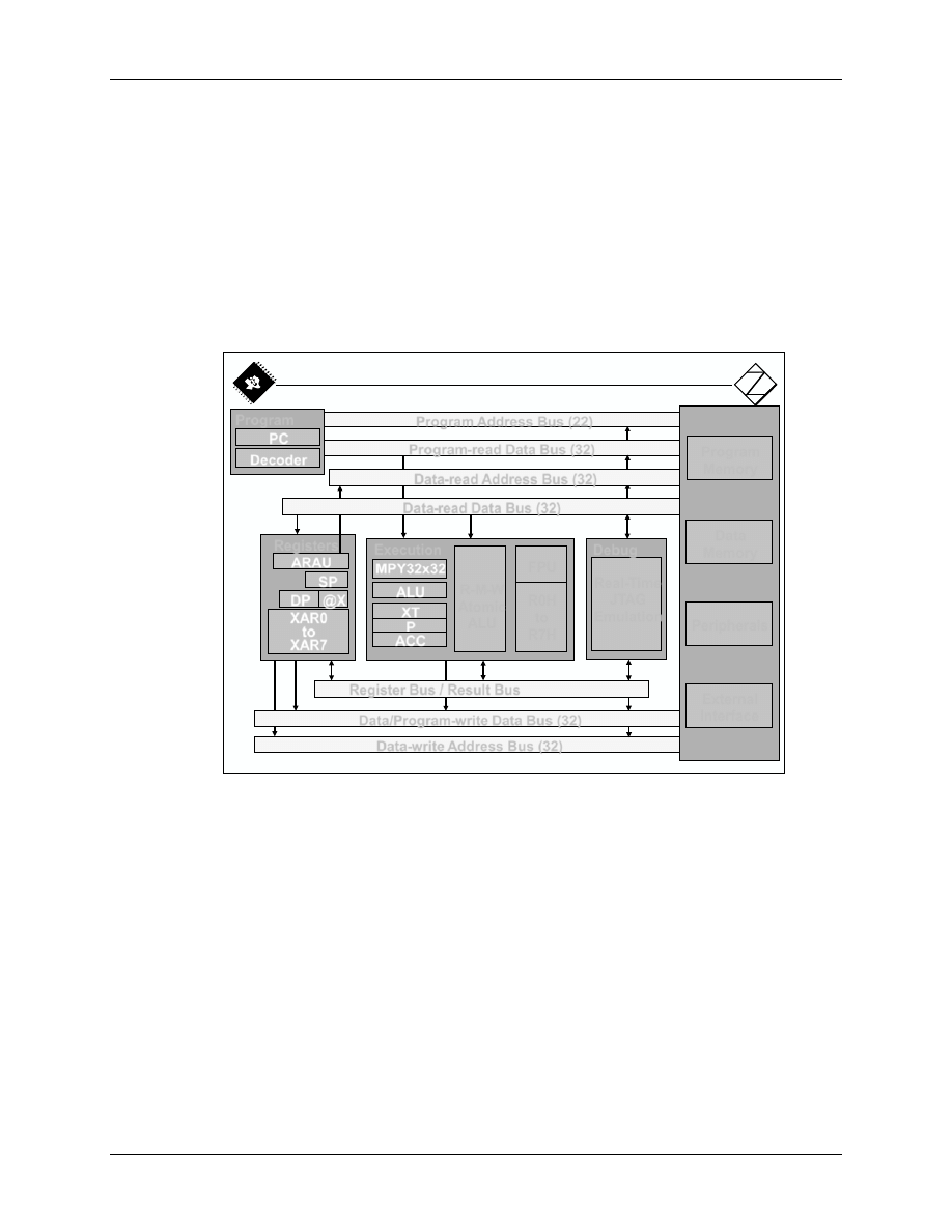
Internal Bus Structure
A typical feature of Digital Signal Processors is their ability to increase the data throughput based
on multiple busses. Such busses are used to move data between memory locations, peripheral
units and the CPU. The F2833x memory bus architecture contains:
•
A program read bus (22-bit address line and 32-bit data line)
•
A data read bus (32-bit address line and 32-bit data line)
•
A data write bus (32-bit address line and 32-bit data line)
•
A register bus (32-bit data line and direct register addressing)
2 - 7
Program-read Data Bus (32)
Data-write Address Bus (32)
Program Address Bus (22)
Execution
R-M-W
Atomic
ALU
Real-Time
JTAG
Emulation
Program
Decoder
PC
XAR0
to
XAR7
SP
DP @X
ARAU
MPY32x32
XT
P
ACC
ALU
Registers
Debug
Register Bus / Result Bus
Data/Program-write Data Bus (32)
Data-read Address Bus (32)
Data-read Data Bus (32)
FPU
R0H
to
R7H
Program
Memory
Data
Memory
Peripherals
External
Interface
F2833x Internal Bus Structure
The 32-bit wide data busses allow single cycle 32-bit operations. This multiple bus architecture,
known as a Harvard Bus Architecture enables the F2833x to (1) fetch an instruction, (2) read a
first data value and (3) write a second data value all within in a single clock cycle.
All registers to control peripheral units are mapped into specific locations in data memory space
and can be accessed with an ordinary data memory write or read instruction. For important pe-
ripheral registers, some security mechanisms are implemented to prevent a modification by acci-
dent.
All internal memory sections are attached both to program and data memory (called "unified
memory model"). It allows the designer to select a certain part to be used as code or as a data sec-
tion.
Module Topics
F2833x - Architecture
2 - 9
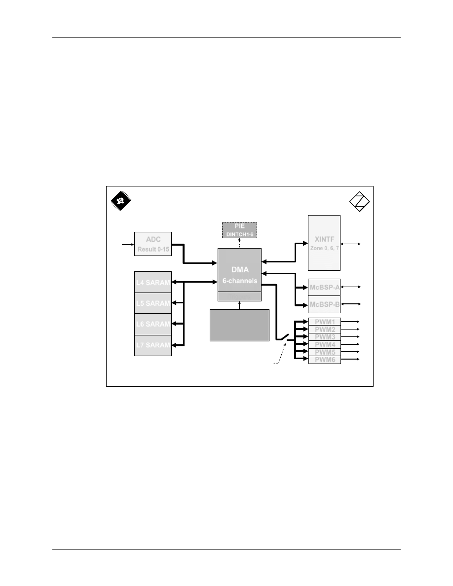
Direct Memory Access Controller (DMA)
A Direct Memory Access Controller has been introduced in the F2833x family. A DMA unit al-
lows a data transfer from a source to a destination unit without the need of an interaction of the
CPU. The strength of a digital signal controller (DSC) is not measured purely in processor speed,
but also in total system capability. As a part of the equation, whenever the CPU bandwidth for a
given function can be reduced, the greater the system capability. Very often applications spend a
significant amount of their bandwidth moving data, whether it is from off-chip memory to on-
chip memory or from a peripheral such as an analog-to-digital converter (ADC) to RAM, or even
from one peripheral to another. Furthermore, there are times when this data comes in a format
that is not compatible with the optimum processing powers of the CPU. The DMA module has
the ability to free up CPU bandwidth and rearrange the data into a pattern for more streamlined
processing.
2 - 8
McBSP-A
McBSP-B
XINTF
Zone 0, 6, 7
DMA
6-channels
L4 SARAM
L5 SARAM
L6 SARAM
L7 SARAM
ADC
Result 0-15
Triggers
SEQ1INT / SEQ2INT
MXEVTA / MREVTA
MXEVTB / MREVTB
XINT1-7 / 13
TINT0 / 1 / 2
PIE
DINTCH1-6
PWM1
PWM2
PWM3
PWM4
PWM5
PWM6
SysCtrlRegs.MAPCNF.bit.MAPCNF
(re-maps PWM regs from PF1 to PF3)
F2833x Direct Memory Access
The DMA module is an event-based machine, meaning it requires a peripheral interrupt trigger to
start a DMA transfer, such as:
•
Analogue to Digital Converter Sequencer 1 (SEQ1INT) or Sequencer 2 (SEQ2INT)
•
Multichannel Buffered Serial Port A and B (McBSP-A, McBSP-B) transmit and receive
•
External Interrupt Input Signals XINT1-7 and XINT13
•
CPU Timers 0, 1 and 2
•
Pulse Width Module (PWM) signals ePWM1-6
•
Software
As data sources and/or destinations that can be initialized:
•
Internal SARAM sections L4 to L7
•
All external memory zones XINTF
•
ADC result registers (source only)
•
McBSP-A and McBSP-B transmit and receive buffers
•
PWM units 1-6 (destination only)
Module Topics
2 - 10
F2833x - Architecture
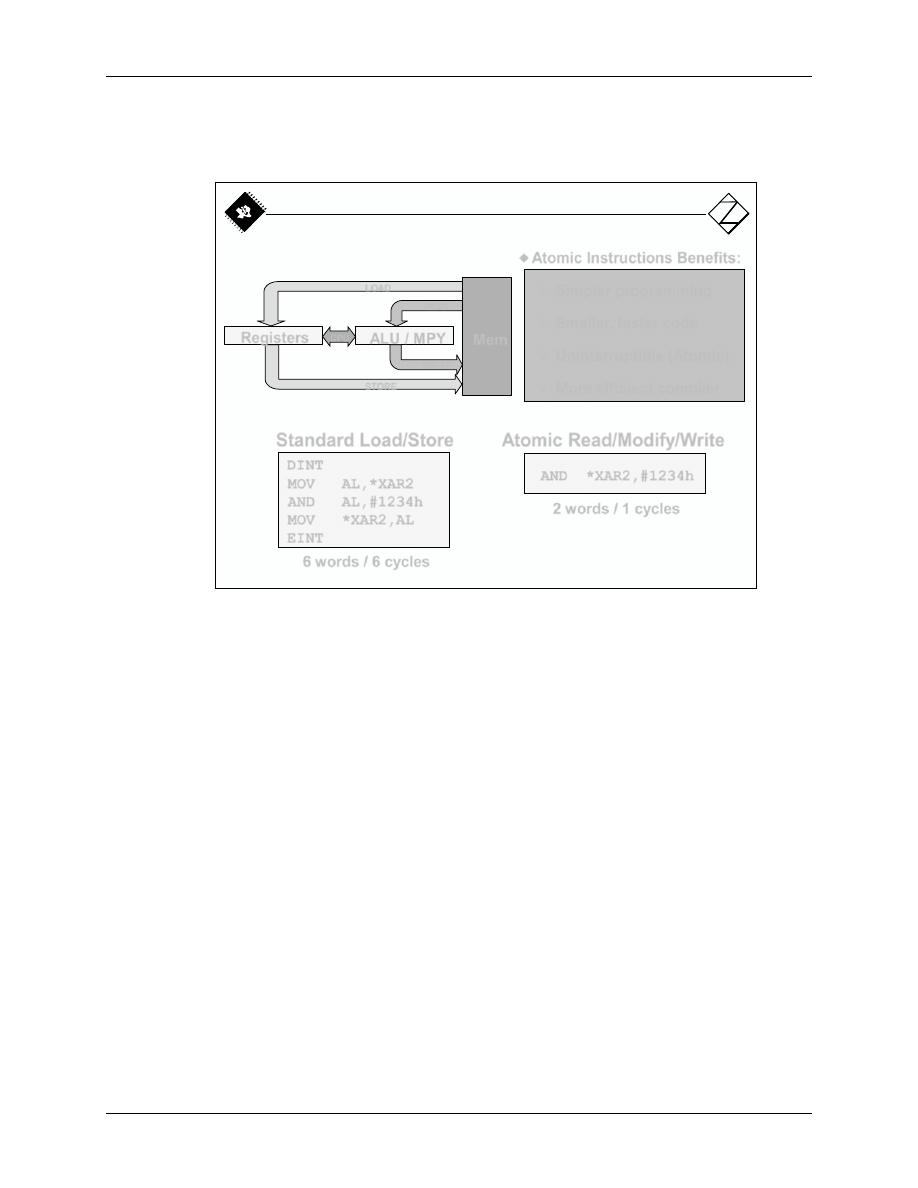
Atomic Arithmetic Logic Unit (ALU)
2 - 9
F2833x Atomic Read/Modify/Write
Registers
ALU / MPY
LOAD
STORE
WRITE
READ
CPU
Mem
Atomic Instructions Benefits:
Simpler programming
Smaller, faster code
Uninterruptible (Atomic)
More efficient compiler
AND *XAR2,#1234h
2 words / 1 cycles
Atomic Read/Modify/Write
MOV
AL,*XAR2
AND
AL,#1234h
MOV
*XAR2,AL
DINT
EINT
6 words / 6 cycles
Standard Load/Store
Atomic instructions are common with embedded system controllers. Examples are logical opera-
tions, such as AND, OR and EXOR directly performed in data memory locations. Usually, these
instructions must be executed without an interruption between read and write accesses; they are
called "non-interruptible" or "atomic" instructions. The F2833x atomic Arithmetic Logic Unit
(ALU) capability supports such types of instructions; as shown on the right hand side of Slide 2-
9.
By contrast, the traditional coding (left hand side of Slide 2-9) would execute several cycles
slower than atomic instructions.
Module Topics
F2833x - Architecture
2 - 11
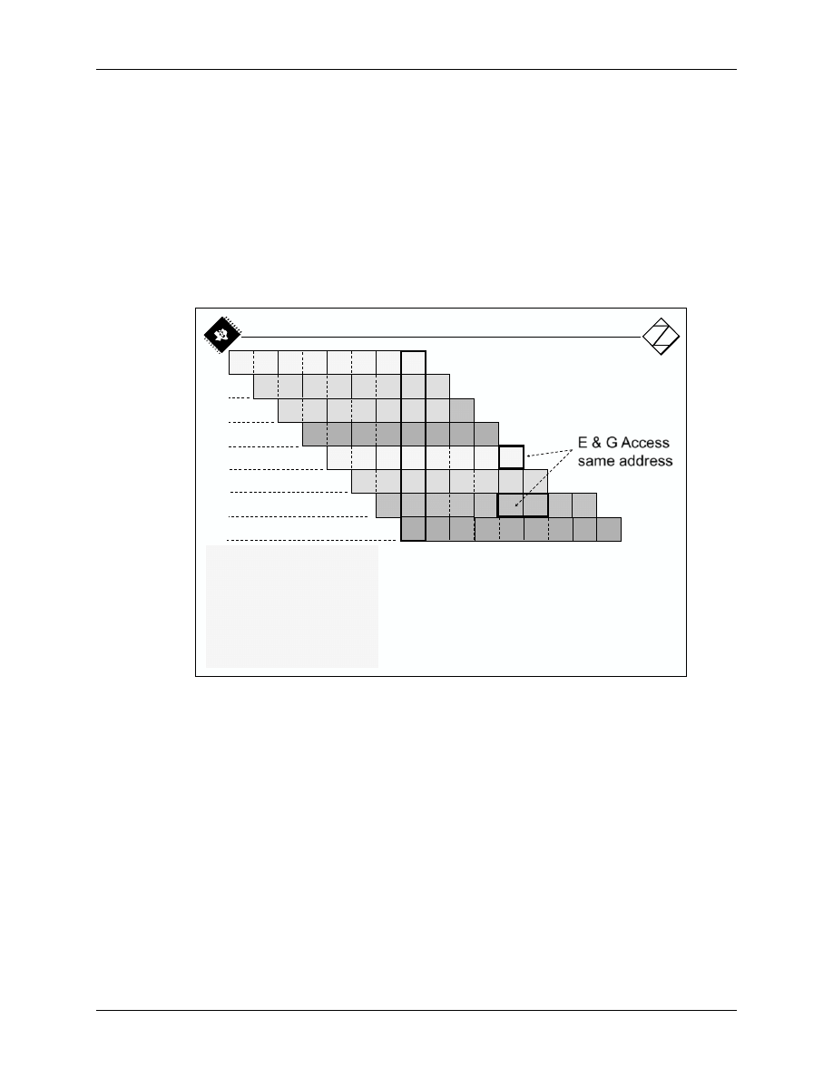
Instruction Pipeline
Like almost all today's microprocessors that operate in speed regions above 50 MHz the F2833x
also uses a pipeline technique to maximize the code throughput. The F2833x features an 8-stage
protected pipeline. The adjective "protected" means that the pipeline unit itself automatically pre-
vents a "write to" and a "read from" the same location from occurring out of sequence (see in-
structions E and G in Slide 2-10). This pipelining also enables the F283xx to execute at high
speeds without resorting to expensive high-speed memories. An additional branch-look-ahead
hardware minimizes the delay when jumping to another address. Particular assembly instructions
called "conditional store operations" avoid pipeline stalls and further improve the overall system
performance.
2 - 10
F
1
F
2
D
1
D
2
R
1
R
2
E
F
1
F
2
D
1
D
2
R
1
R
2
E
F2833x Pipeline
Protected Pipeline
Order of results are as written in
source code
Programmer need not worry about
the pipeline
8-stage pipeline
F
1
F
2
D
1
D
2
R
1
R
2
E
F
1
F
2
D
1
D
2
R
1
R
2
E
F
1
F
2
D
1
D
2
R
1
R
2
E
F
1
F
2
D
1
D
2
R
1
R
2
E
F
1
F
2
D
1
D
2
R
1
R
2
E
F
1
F
2
D
1
D
2
R
1
R
2
E
A
B
C
D
E
F
G
W
W
W
W
W
W
W
W
E & G Access
same address
R
1
R
2
E W
D
2
R
1
R
2
E W
F1: Instruction Address
F2: Instruction Content
D1: Decode Instruction
D2: Resolve Operand Addr
R1: Operand Address
R2: Get Operand
E: CPU doing “real” work
W: store content to memory
H
Each instruction passes through 8 stages until final completion. Once the pipeline is filled with
instructions, one instruction is executed per clock cycle. For a 150MHz device, this equates to
6.67ns per instruction.
The stages are:
F1:
Generate Instruction Address at program bus address lines.
F2:
Read the instruction from program bus data lines.
D1:
Decode Instruction
D2:
Calculate Address information for operand(s) of the instruction
R1:
Load operand(s) address to data and/or program bus address lines
R2:
Read Operand
X:
Execute the instruction
W:
Write back result to data memory
Module Topics
2 - 12
F2833x - Architecture
Memory Map
The memory space of the F2833x is divided into program space and data space. There are several
different types of memory available that can be used as both a program or a data space member.
These include independent sections of flash memory, single access RAM (SARAM), one time
programmable memory (OTP) and boot ROM. The latter is factory programmed with boot soft-
ware routines and trigonometric lookup tables used in maths based algorithms. Memory space
width is always 16 bits.
2 - 11
XINTF Zone 6 (1Mw)
XINTF Zone 7 (1Mw)
0x000000
0x000400
0x000800
M1 SARAM (1Kw)
M0 SARAM (1Kw)
Data Program
PIE Vectors
(256 w)
PF 0 (6Kw)
XINTF Zone 0 (4Kw)
reserved
PF 1 (4Kw)
PF 2 (4Kw)
PF 3 (4Kw)
L0 SARAM (4Kw)
L1 SARAM (4Kw)
L2 SARAM (4Kw)
L3 SARAM (4Kw)
L4 SARAM (4Kw)
L5 SARAM (4Kw)
L6 SARAM (4Kw)
L7 SARAM (4Kw)
reserved
0x000D00
0x002000
0x006000
0x007000
0x008000
0x009000
0x00A000
0x00C000
0x000E00
0x005000
0x00B000
0x00D000
0x00E000
0x00F000
0x004000
0x010000
0x010000
0x100000
0x200000
reserved
Data Program
FLASH (256Kw)
0x300000
0x33FFF8
0x340000
PASSWORDS (8w)
reserved
User OTP (1Kw)
0x380800
ADC calibration data
0x380080
0x380090
reserved
0x380400
reserved
0x3F8000
Boot ROM (8Kw)
L0 SARAM (4Kw)
L1 SARAM (4Kw)
L2 SARAM (4Kw)
L3 SARAM (4Kw)
reserved
0x3F9000
0x3FA000
0x3FB000
0x3FC000
0x3FE000
0x3FFFFF
DMA Accessible:
L4, L5, L6, L7,
XINTF Zone 0, 6, 7
Dual Mapped:
L0, L1, L2, L3
CSM Protected:
L0, L1, L2, L3,
FLASH, ADC CAL,
OTP
0x3FFFC0
BROM Vectors (64w)
TMS320F2833x Memory Map
The F2833x can access memory both on and off the chip. The F2833x uses 32-bit data addresses
and 22-bit program addresses. This allows for a total address reach of 4G words (1 word = 16
bits) in data space and 4M words in program space. Memory blocks on all F2833x designs are
uniformly mapped to both program and data space.
The memory map above shows the different blocks of memory available to the program and data
space.
The non-volatile internal memory consists of a group of FLASH-memory sections, a boot-ROM
for up to 12 reset-startup options and a one-time-programmable (OTP) area. FLASH and OTP are
usually used to store control code for the application and/or data that must be present at reset. To
load information into FLASH and OTP, a dedicated download program is needed, which is also
part of the Texas Instruments Code Composer Studio integrated design environment.
Volatile Memory is split into 10 areas called M0, M1 and L0 to L7 that can be used both as code
memory and data memory.
PF0, PF1 and PF2 are Peripheral Frames that cover control and status registers of all peripheral
units (“Memory Mapped Registers”).
Module Topics
F2833x - Architecture
2 - 13
Code Security Module
There is an internal security module available in all F2833x family members. It is based on a 128-
bit password that is written by the software developer into the last 8 memory spaces of the
internal FLASH (0x3F 7FF8 to 0x3F 7FFF). Once a pattern is written into this area, all further
accesses to any of the memory areas covered by this Code Security Module (CSM) are denied, as
long as the user does not write an identical pattern into password registers of frame PF0.
NOTE: If you write any pattern into the password area by accident, there is no way to get access
to this device anymore! Also, any attempt to re-flash a secured device will fail.
So please be careful and do not upset your laboratory technician!
2 - 12
Code Security Module
Prevents reverse engineering and
protects valuable intellectual property
128-bit user defined password is stored in Flash
128-bits = 2
128
= 3.4 x 10
38
possible passwords
To try 1 password every 2 cycles at 150 MHz, it
would take at least 1.4 x 10
23
years to try all
possible combinations!
CSM Protected:
L0, L1, L2, L3,
FLASH, ADC CAL,
OTP
The purpose of a password secured device is to prevent reverse engineering of a control system.
The code security module will deny any unauthorized access attempts and will protect your
intellectual property (IP).
Module Topics
2 - 14
F2833x - Architecture
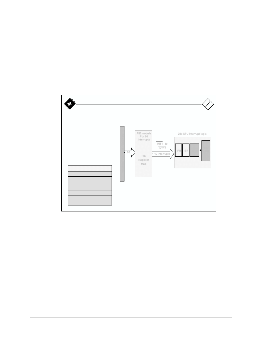
Interrupt Response
A key feature of a control system is its ability to respond to asynchronous external hardware
events as quickly as possible. The F2833x combines such fast interrupt responses with an auto-
matic “context” save of critical CPU registers, which allows the service of many asynchronous
events with minimal latency. Here “context” means all the registers that need to be saved so that
you can go away and carry out some other process, then come back to exactly where you left.
F2833x devices implement a zero cycle penalty to save and restore the 14 registers during an in-
terrupt. This feature helps to reduce the interrupt service routine overheads.
2 - 13
F2833x Fast Interrupt Response Manager
96 dedicated PIE
vectors
No software decision
making required
Direct access to RAM
vectors
Auto flags update
Concurrent auto
context save
28x CPU Interrupt logic
28x
CPU
INTM
IFR
IER
96
P
er
ip
h
er
al
I
n
ter
ru
p
ts
12x8
=
96
12 interrupts
INT1 to
INT12
PIE
Register
Map
PIE module
For 96
interrupts
T
ST0
AH
AL
PH
PL
AR1 (L)
AR0 (L)
DP
ST1
DBSTAT
IER
PC(msw) PC(lsw)
Auto Context Save
We will look in detail into the F2833x interrupt system in Module 6 of this tutorial. The
Peripheral Interrupt Expansion (PIE) - Unit allows the user to specify individual interrupt service
routines for up to 96 internal and external interrupt events. All possible 96 interrupt sources share
14 maskable interrupt lines (INT1 to INT14), 12 of them are controlled by the PIE - module.
The auto context save loads 14 important CPU registers, as shown in Slide 2-13 above, into a
stack memory, which is pointed to by a stack pointer (SP) register. The stack is part of the data
memory and must reside in the lower 64K words of data memory.
Module Topics
F2833x - Architecture
2 - 15
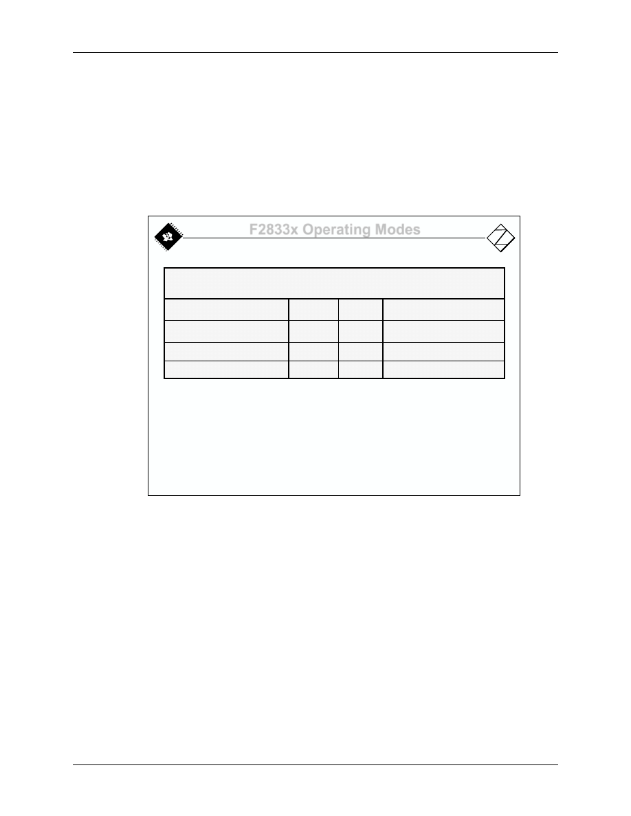
Operating Modes
The F2833x is a member of the TMS320C2000 family of Digital Signal Controllers (DSCs). This
family consists both of 32-bit fixed-point and floating-point devices and also of 16-bit members.
The Test Mode is used for fabrication test purposes only. The F2833x can be switched from its
native mode into an operating mode, that is source code compatible with the 16-bit group
C24x/C240x. Code, which has been previously written for a C24x device, can be reassembled to
run on a F2833x device. This allows for migration of existing code onto the F2833x.
2 - 14
F2833x Operating Modes
C28x Native Mode
1
0
C24x Compatible Mode
1
1
Test Mode (default)
0
0
Reserved
0
1
OBJMODE AMODE
Mode Bits
Compiler Option
Mode Type
Almost all uses will run in C28x Native Mode
The bootloader will automatically select C28x Native Mode after reset
C24x compatible mode is mostly for backwards compatibility with an
older processor family
-v28 –m20
-v28
In fact, the F2833x silicon is able to operate in three different modes:
•
C28x - Mode
- takes advantage of all 32-bit features of the F2833x device
•
C24x - Mode
- source code compatibility to the 16-bit family members
•
Test - Mode
- intermediate operating mode, test purposes only.
After RESET, the device is set into test mode. To take advantage of the full computing power of
an F2833x device, the control flag “OBJMODE” must be set to 1 to switch into F2833x native
mode. If you start the execution of your code from the boot code entry point, the boot code will
set that bit for you.
Module Topics
2 - 16
F2833x - Architecture
Reset Behaviour
After a valid RESET-signal is applied to the F2833x, the following sequence depends on some
external pins on this DSC.
An active RESET signal will read the first address to be loaded into the Program Counter register
(PC) from address 0x3F FFC0, which is in boot memory. The value inside this address is the
address of the beginning of the boot code sequence. As a result, the F2833x jumps directly to the
internal boot code memory. This code has been developed by TI to be able to distinguish
between 12 different start options for the F2833x. The active option is derived from the status of
4 general-purpose input pins (GPIO) at this very moment. For our tutorial we use the volatile
memory M0 as code memory and its first address as the execution entry point.
2 - 15
Reset
OBJMODE = 0 AMODE = 0
ENPIE = 0 INTM = 1
Boot determined by
state of GPIO pins
Reset vector fetched
from boot ROM
0x3F FFC0
Execution
Entry Point
M0 SARAM
Note:
Details of the various boot options will be
discussed in the Reset and Interrupts module
Bootloader sets
OBJMODE = 1
AMODE = 0
Reset – Bootloader

Module Topics
F2833x - Architecture
2 - 17
Summary of TMS320F2833x Architecture
3
3
-
-
16
16
High performance 32
High performance 32
-
-
bit DSP
bit DSP
32x32 bit or dual 16x16 bit MAC
32x32 bit or dual 16x16 bit MAC
IEEE single
IEEE single
-
-
precision floating point unit
precision floating point unit
Atomic read
Atomic read
-
-
modify
modify
-
-
write instructions
write instructions
Fast interrupt response manager
Fast interrupt response manager
256Kw on
256Kw on
-
-
chip flash memory
chip flash memory
Code security module (CSM)
Code security module (CSM)
Control peripherals
Control peripherals
12
12
-
-
bit ADC module
bit ADC module
Up to 88 shared GPIO pins
Up to 88 shared GPIO pins
Watchdog timer
Watchdog timer
DMA and external memory interface
DMA and external memory interface
Communications peripherals
Communications peripherals
Summary

Module Topics
2 - 18
F2833x - Architecture
This page has been intentionally left blank.
Document Outline
- Architecture
- Introduction
- Module Topics
- TMS320F2833x Block Diagram
- Bus System
- Central Processing Unit (CPU)
- Fixed-point Math Unit
- Floating-point Math Unit
- Data Memory Access
- Internal Bus Structure
- Direct Memory Access Controller (DMA)
- Atomic Arithmetic Logic Unit (ALU)
- Instruction Pipeline
- Memory Map
- Code Security Module
- Interrupt Response
- Operating Modes
- Reset Behaviour
- Summary of TMS320F2833x Architecture
Wyszukiwarka
Podobne podstrony:
Module 02
Assertivness Module 02
CE Elementary module 02 web worksheet
02 cisco semestr 3 v31 module 2 exam
02 cisco semestr 2 v31 module 2 exam
02 BS Module 1 Section 2
Wyk 02 Pneumatyczne elementy
02 OperowanieDanymiid 3913 ppt
02 Boża radość Ne MSZA ŚWIĘTAid 3583 ppt
OC 02
PD W1 Wprowadzenie do PD(2010 10 02) 1 1
02 Pojęcie i podziały prawaid 3482 ppt
WYKŁAD 02 SterowCyfrowe
więcej podobnych podstron