International Rectifier
•
233 Kansas Street El Segundo CA 90245 USA
Fluorescent Ballast Design Using Passive P.F.C. and Crest Factor Control
by
Peter N. Wood
I. INTRODUCTION
Power quality standards are being imposed
worldwide in order to maximize the efficiency of the
existing total generation capacity. Adding additional
generating capacity is increasingly difficult and expensive
because of environmental constraints so the onus for
improved efficiency falls on the power user rather the
power supplier.
Off-line power converters of which electronic
ballasts are a major category, are no longer permitted to
present low power factor and high harmonic currents to the
electric power grid. Indeed all classes of user equipment
from motors to T.V. sets and computers are now , or soon
will be regulated by power quality specifications.
Table 1 - IEC1000-3 LIMITS FOR CLASS C EQUIPMENT
Harmonic Order
(n)
Maximum Value Expressed as a
Percentage of the Fundamental
Input Current of Lumineres
2
2
3
30 x
λ
5
10
7
7
9
5
11
≤
n
≤
39
3
Electronic ballasts are generally required to
comply with power quality specifications such as IEC
1000-3 which mandate maximum limits for harmonic
currents out to the 39th harmonic (see Table 1).
Other countries will issue similar power quality
specifications to the European IEC1000 standard so it is
expected that the worldwide lighting market will have
similar requirements.
II. POWER FACTOR CONTROL METHODS:
There are two basic categories of power factor
improvement circuits namely active and passive. A typical
active P.F.C. circuit supplies a regulated DC bus at higher
voltage then the maximum peak voltage of the AC supply
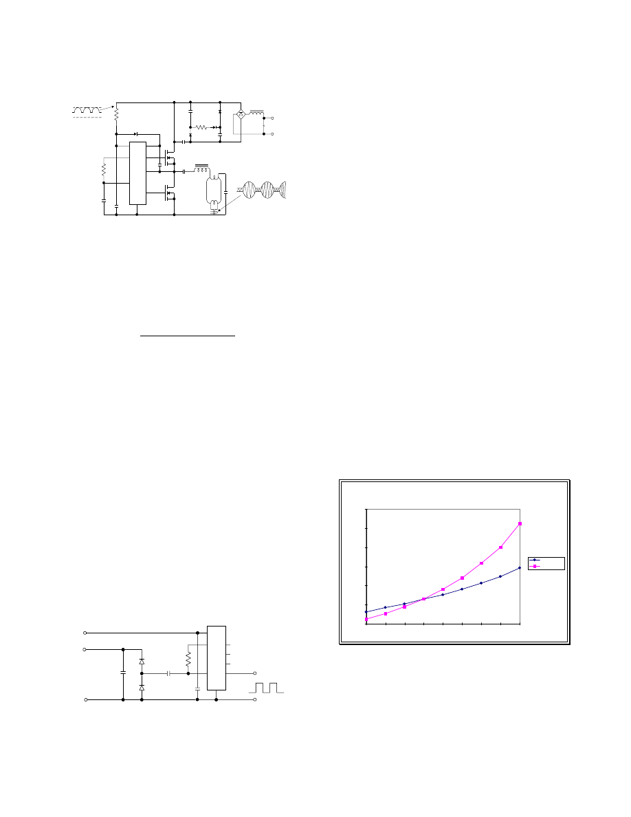
and uses a simple boost topology as shown in Fig. 1.
The boost topology of Fig. 1 may be operated at
constant high frequency with continuous inductor current
or in the critical conduction mode where the inductor is
allowed to discharge to zero energy in before initiating a
new charge cycle. Most of the commercially available
control IC’s are of the latter type. The active PFC circuit
is entirely satisfactory for harmonic compliance but the
cost of the additional circuitry is often unacceptable in
many low cost mass market ballast applications.
Fig. 1 - Active PFC Circuit
A
PPLICATION
N
OTE
AN998
DC Output
PFC Drive
+
+
-
L
pw-fig01.vsd

pw-fig02.vsd
AC Input
DC Output
+
-
Fig. 2 - L-C Passive PFC Circuit
Passive PFC circuits on the other hand operate at
mains frequency (50 or 60Hz) using capacitors and iron cored
inductors tuned to the line frequency in a low pass or band
pass configuration. Unfortunately the physical size and
weight of these filters at mains frequency makes them unat-
tractive, especially when one considers that the rest of the
ballast circuitry can be smaller than the PFC components!
Another novel way to achieve power factor improve-
ment to >95% using simple, low cost circuitry is shown in
Fig. 3.
In this circuit the filter capacitors are charged in
series via the diode and resistor on each half cycle of the
rectified AC input. Each capacitor is charged to ½ of the AC
peak voltage, minus three diode drops - two in the bridge
rectifier and one in the diode between the two capacitors.
The purpose of the resistor is to reduce the peaks in the cur-
rent waveform as the capacitors charge.
Since each capacitor is charged to half the peak AC
voltage, they supply output current only after the bus volt-
age follows the sinusoidal waveform down to V
peak
/2. At
this time the capacitors are essentially in parallel and supply
load current until the rectified AC input again exceeds V
P
/2
on the next half cycle. The discharge duty cycle for the
capacitors is approximately 37% followed by an idle period
during which time the load is being supplied directly from
the rectified AC input. At the peak of the input AC voltage
there is an additional current to re-charge the capacitors up
to V
peak
. The magnitude and duration of this current is a
function of the depth of discharge and the value of the resis-
tor in the charging circuit.
The L-C circuit at the AC input is a filter for in-
verter switching spikes which otherwise would appear on
the AC input lines. It also smoothes out the steps in the
current waveform of the passive PFC, valley fill circuit.
DC Output
AC Input
+
-
pw-fig03.vsd
+
+
Fig. 3 -50% Valley Fill Passive PFC Circuit
Although the circuit presents a reasonably good
Power Factor (>0.95) and the harmonics can be tamed by
the L-C input filter, the major shortcoming of this circuit is
the 50% bus ripple voltage which, in a typical ballast cir-
cuit, results in a crest factor exceeding 2.1.
NOTE: Lamp manufacturers recommend a C.F. =
1.7 max and even that may result in a somewhat reduced
lamp life.
There are many low cost ballast designs similar to
Fig. 4 in production today. Some are driven by self-oscillat-
ing drivers such as the IR2153. Others use the familiar cur-
rent transformer drive, but all have a similar lamp current
waveform envelope. A lamp life expectancy <5000 hours is
typical of such circuits even when pre-heating is used dur-
ing lamp start-up. NOTE: When measuring lamp current in
this circuit, both cathode leads pass through the current probe.
The lamp filament current is balanced out and only the ac-
tual lamp arc current is measured.
It is immediately apparent that lamp current is di-
rectly proportional to lamp voltage and hence DC bus volt-
age. Lamp life is shorted not only by the 50% valley fill
PFC but by variations in actual AC line voltage. Thus a
ballast designed to supply rated lamp power at nominal AC
line will have reduced light output at low line and reduced
lamp life at high line.
What is needed, therefore, is a low cost ballast which
maintains constant lamp current over the entire AC line volt-
age range (line swings of 150VAC-270VAC are not uncom-
mon in some areas of the world) but also has a current sense
circuit fast enough to respond to and regulate the 120Hz
50% Valley Fill waveform.
pw-fig04.vsd
IR2153
Current Probe
+
C
T
R
T
Current Envelope
CF > 2.1
C
+
AC Input
+
V
CC
R
T
V
B
C
T
L
o
H
o
V
S
COM
L
V
P
= 320V
0
V
P
/2
Fig. 4 - Electronic Ballast without Crest Factor Control
Reference to Fig. 4 shows a simple self-oscillating
ballast circuit where the switching frequency is determined
by the values of RT and CT and given by the equation:
(
)
f
C
T
R
T
sw
=
+
1
1 38
75
.
Ω
Fig. 4 is a fixed frequency application without pro-
visions for lamp filament pre-heating and is consequently
not recommended for use in any ballasts where lamp life is a
consideration.
Pre-heat in fluorescent ballasts can be accomplished
by applying a higher than operating frequency to the lamp
circuit for a timed period, usually about 1 second and then
reducing the frequency towards resonance to permit lamp
starting with hot filaments.
An oscillator circuit as shown in Fig. 5 has a VCO
function when an offset voltage is applied to the timing ca-
pacitor. The following explanation of circuit operation will
clarify this function.
III. THE VCO FUNCTION USING IR215X CONTROL
IC’S:
+ V
CC
DC Offset Bias
pw-fig05.vsd
V
C C
R
T
V
B
C
T
L
o
H
o
V
S
C O M
IR2153
V
o
COM
0.1
µ
F
IN4148
IN4148
C
T
R
T
10K
+
1nF
Fig. 5 - Frequency Control by Offset Bias Voltage
IR2155, 2151, 2152, 2153 are all self-oscillating
level shifting driver IC’s incorporating an oscillator similar
to the ever popular 555 timer IC.
The oscillator uses a timing capacitor and resistor
and switches when the capacitor is charged and discharged
to voltages of 1/3 V
CC
and 2/3 V
CC
. The IR215X control IC’s
are all provided with an internal V
CC
zener clamp at about
15.6 VDC so the actual C
T
pin switch levels are 5.1 and
10.2V respectively, which means that the timing capacitor
is charged and discharged 10.2 - 5.1V or 5.1 volts swing to
reach each switching voltage.
By adding an AC offset voltage to the timing cir-
cuit, the actual voltage change on the timing capacitor is
reduced by the magnitude of the offset voltage. Thus with
an offset voltage of 3 volts, for example, the capacitor charges
and discharges by 5.1-3 = 2.1 volts. It is obvious therefore
that a
∆
V of 2.1 volts takes less time than a 5.1 volts
∆
V.
Since R
T
and V
CC
are constant, it can readily be seen
that the time to reach the switching levels of 5.1 and 10.2
volts is reduced by about 60%, hence the switching fre-
quency must also increase by 60%.
It is also apparent that the AC offset voltage is the
DC offset bias + 2V
F
of the IN4148 diodes. NOTE also that
as the DC offset bias is changed, the lower end of C
T
takes
on a DC bias but the incremental charge is not affected by
this.
Fig. 6 - Frequency vs. DC Offset Bias
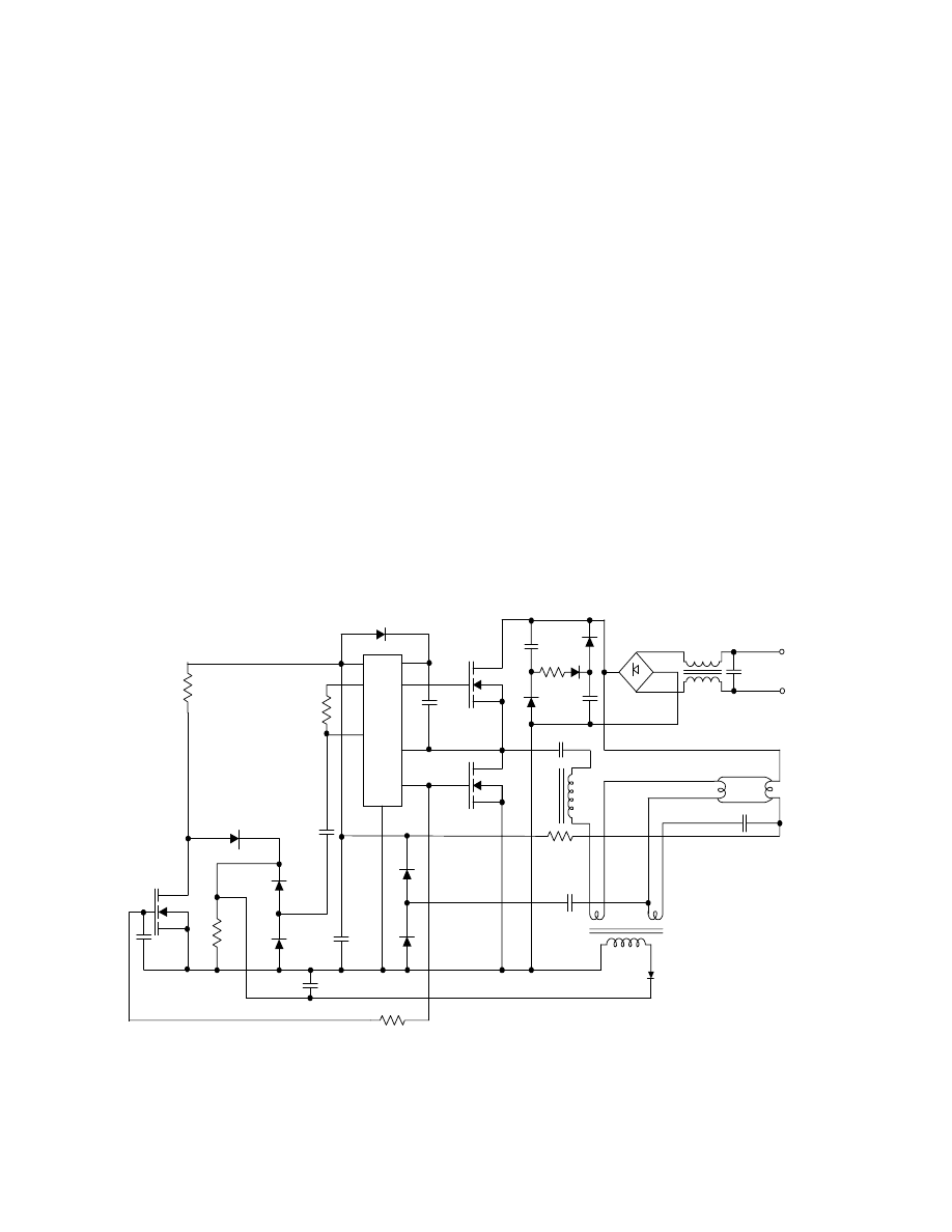
The graphs of Fig. 6 are exponential curves as is
the charge on C
T
when charged through R
T
from a fixed volt-
age V
CC
. Because of this non-linearity, the offset voltage
control technique is not suitable for open loop applications
which would use a fraction of the rectified bus voltage of
Fig. 4 as a control parameter.
Voffset VS. Fs
IR2153
60000
70000
80000
90000
100000
110000
120000
-0.6V
-0.4V
-0.2V
0.0V
0.2V
0.4V
0.6V
0.8V
1.0V
Voffset
Fs (Hz)
Vcc = 15.5V
Vcc = 9V
However, when used in a closed loop application
where the control parameter is lamp current, the non-lin-
earity becomes a second order variable provided there is
sufficient loop gain to swamp out the second order effect.
In terms of temperature stability, the two diodes
in the offset circuit tend to reduce the AC offset at high
temperature thus slightly reducing the frequency. This
shift can be compensated by rectifying the lamp current
waveform with a similar diode which tends to increase
the DC sense voltage and with it the operating frequency.
The circuit shown in Fig. 7 shows how this is
accomplished and yields a frequency vs. Lamp current
control with close to zero temperature coefficient.
Using the control technique described above, it
is possible to design fluorescent ballasts with power fac-
tor >0.95, THD <15% (c.f. Table 1 values), lamp crest
factor <1.7 without the additional complexity and cost of
an active boost topology PFC circuit and that also accom-
modates a wide range of AC input voltage since the con-
trol parameter is lamp current only.
Of course, since the lamp current is being regulated
by this circuit, it is only a short step to substitute a variable
current sense resistor to obtain a lamp dimming function
which still retains pre-heating but additionally will start and
operate at any dimmed setting.
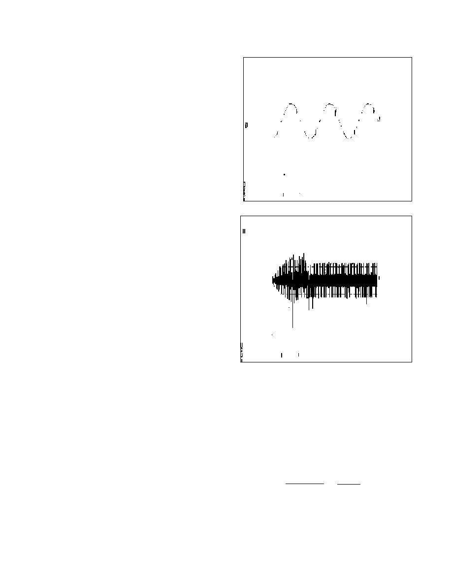
The circuit of Fig. 7 operates over a very broad range
of AC input voltage and provides tight regulation of the light
output. The 50% valley fill, passive PFC circuit as shown in
Fig. 3, is used to provide the positive bus which has a ripple
voltage swing of 160V to 330V at twice mains frequency.
A small current transformer is used to sense lamp
arc current and although this looks complicated referring to
Fig. 7 it really is just a single winding toroid with both cath-
ode leads passed through the toroid to form single turn op-
posing windings. In operation the opposing windings can-
cel out the filament currents leaving only the arc current as
the measured parameter. The toroid itself is a small ferrite
core such as those used in transformer driven ballast circuits
costing about $0.10
pw dis f0 9.vs d
230VAC
4 X 1N4007
5+5mH
5
C
T
L
O
COM
R
T
V
C C
V
B
H
O
V
S
6
7
8
1
2
3
4
150K
10DF6
1N4148
40W
22
1N4007
0.1
µ
400V
1mH
10M
IRF014
47
µ
F
+
16V
2.7K
1N4148
1N4148
0.1
µ
F
1N4148
220PF
1N4007
0.1
µ
12K
3 X 1N4007
+
+
47
µ
250V
47
µ
F
250V
22 1W
470 PF
630V
0.033
µ
F
IRF820
+
IRF820
0.0q
µ
F
630V
Polyprop.
0.01
µ
F
250VAC
Fig. 7 Using Lamp Current Regulation to Implement a 40W ballast with
pre-heat, 0.96PF and input Voltage Range from 180 to 280VAC
The secondary winding produces a voltage across a
2.7k resistor proportional to lamp current and this voltage is
used as the offset bias to control oscillator frequency as de-
scribed in Fig. 5.
The control circuit time constant is less than 100mS
which is fast enough to regulate the current waveform to the
instantaneous values of the 50% valley fill voltage. The con-
trol loop achieves lamp crest factor control at about 1.6 ver-
sus over 2.1 without lamp current regulation.
IV.
PRE-HEAT:
The DC offset bias can also be used to control fre-
quency for pre-heating the lamp. A small N-Channel
MOSFET combined with a 1 second time constant R-C cir-
cuit provides maximum offset bias i.e. maximum operating
frequency during the pre-heat period. As the gate voltage
rises above the threshold voltage V
TH
, the MOSFET slowly
turns on and lowers the operating frequency by reducing the
offset voltage. During this frequency sweep, the lamp soft
starts and the resulting lamp current then controls the offset
voltage in a closed loop mode.
In order to maximize lamp life, the pre-heating of
the lamp filaments must reach 700°C (red heat) at the time
of ignition. The time period for pre-heat is typically one
second or less which makes it important to transfer the maxi-
mum energy in the available time. It would appear that
merely raising the filament voltage is the answer but unfor-
tunately this causes an arc current to flow between the fila-
ment support wires and some point on the filament coil it-
self, causing a point on the filament to glow white lot. This
is very destructive to the lamp and causes the ends of the
lamp to blacken and eventually open circuits one of the fila-
ments at greatly reduced lamp life.
During the pre-heat cycle, the filaments area driven
at constant current with a rising voltage due to the approxi-
mately 4:1 ratio of hot to cold filament resistance. As the
frequency ramps down during the ignition period, the hot
filaments receive an additional boost in voltage as the cir-
cuit approaches resonance. This boost voltage ensures that
the filaments reach the required 700°C when ignition oc-
curs. After ignition the lamp circuit behaves as an inductive
load. The capacitor current is low during normal operation
and the filaments are driven at reduced voltage which maxi-
mizes overall efficiency (see Fig. 8). NOTE: Filament
temperature is largely maintained by arc current during steady
state operation.
Steady State 8.5V Rms
Pre-Heat Soft Strike 1.25Sec
Fig. 8 - Filament Voltage vs. Time
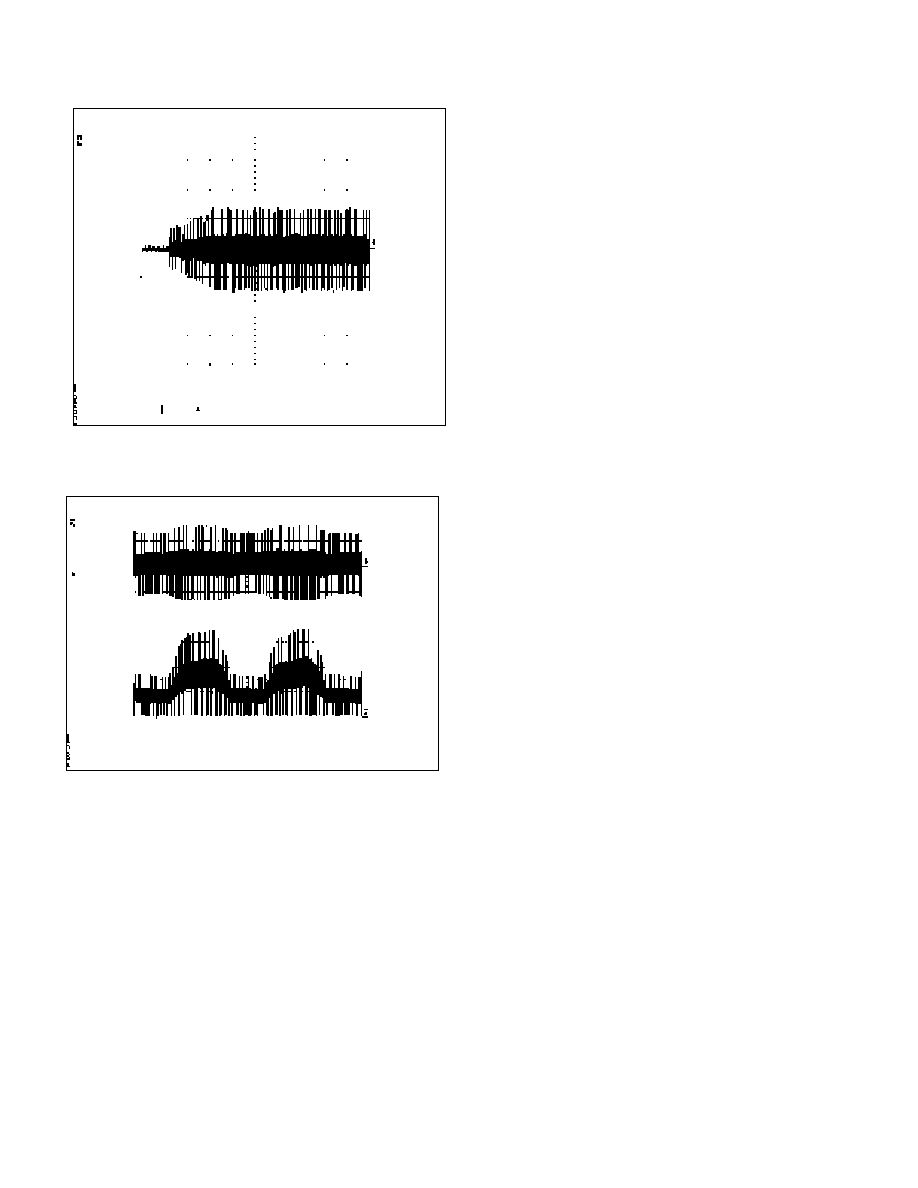
In Fig. 8 note that there is no large spike of current
when the lamp starts which helps to prolong lamp life. The
waveforms of Fig. 9 show an expanded view of the lamp
current at the point of ignition and the gradual increase of
lamp current up to the steady state condition. Also shown is
the regulation of lamp current versus the large 120Hz ripple
on the inverter ½ bridge output.
Measurements of the steady state lamp current waveform
indicate a crest factor < 1.63 where
CF =
Peak Current
Rms Current
≅
130mA
180mA
= 1 625
.
Crest factors less than 1.7 which is the lamp manu-
facturers recommended maximum coupled with soft start-
ing as demonstrated in this ballast result in maximum lamp
life expectancy.
V
V
V
V
V. OPERA
. OPERA
. OPERA
. OPERA
. OPERATION ON 100-120V
TION ON 100-120V
TION ON 100-120V
TION ON 100-120V
TION ON 100-120V A
A
A
A
AC MAINS
C MAINS
C MAINS
C MAINS
C MAINS
The major problem when operating a ballast on 100-
120VAC mains is when the lamp voltage is higher than the
mains voltage. Some method for boosting the high frequency
lamp supply must be used. One such method is to use a
step-up transformer at the output but that adds cost. An-
other method uses the lamp circuit Q factor to boost the volt-
age at frequencies slightly higher than the resonant frequency.
With open loop designs that do not use feedback control,
maintaining this operating point is almost impossible. How-
ever, when using lamp current regulation at the reduced bus
voltages available from 120VAC mains, the operating point
can be stabilized, but at low line there may be insufficient
circuit Q to maintain reliable operation and the lamp extin-
guishes.
For ballast designs used with lamps requiring a
higher operating voltage than the A.C. mains voltage, an
active boost PFC circuit must be used.
In general a higher power lamp means a longer arc
tube because arc current is constant for lamps of the same
tube diameter in a product family. Compact lamps have small
diameter tubes and the total arc length is also small. These
lamps typically operate in the 80-100 V
RMS
range and are
therefore suitable for use with the valley fill, current control
technique operating from 100-120VAC mains. A compact
ballast of this type can operate from universal mains inputs
from 85VAC to 280VAC using 500 volt MOSFETs, although
there is a R
DS(on)
penalty at the lower input voltages by so
doing. It is preferable, therefore, to design for a specific
range of inputs say 85 to 130VAC or 180-280VAC.
Regardless of the PFC circuit design, active or pas-
sive, the regulation of lamp current provides superior lamp
operation and therefore longer lamp life.
Lamp Current Ramp up to Steady State after Soft Strike (100mA/Div)
Lamp Current Ramp up to Steady State after Soft Strike (100mA/Div)
Fig 9-Lamp Current
In Fig 9, note the 50% ripple voltage at the inverter
output. Compare this with the upper waveform. Showing
lamp current being controlled by frequency sweep as de-
scribed in this application note. This current waveform yields
a lamp current crest factor of 1.625.

Wyszukiwarka
Podobne podstrony:
PFC passive Valley fill for flyback
Passive Voice 2
Passive Voice II
PFC
The Passive
Investigations at Souskiou Laona settlement, Dhiarizos Valley, 2005
PASSIVE 1
Changes in passive ankle stiffness and its effects on gait function in
passive voice
Angielski Gramatyka opracowania Passive voice what is it
Passive voice
passive
passiv
2, PASSIVmodal, Futur I Ak
coniugatio periphrastica passiv Nieznany
Tempora Passiv
więcej podobnych podstron