
1
EE462L, Spring 2014
DC−DC Boost Converter
2
V
in
+
V
out
–
C
i
C
I
out
i
in
Buck
converter
i
L
L
+ v
L
–
Boost
converter
V
in
+
V
out
–
C
i
C
I
out
i
in
i
L
L
+ v
L
–
3
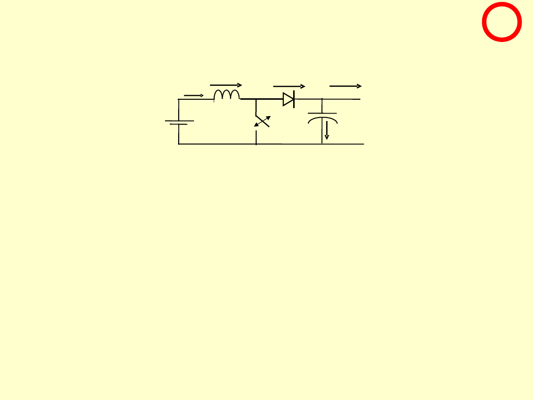
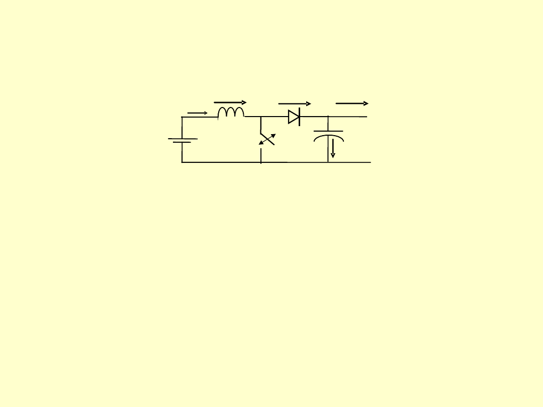
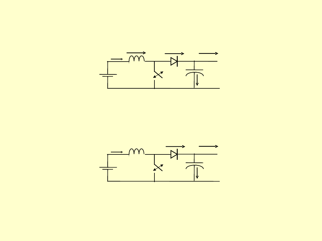
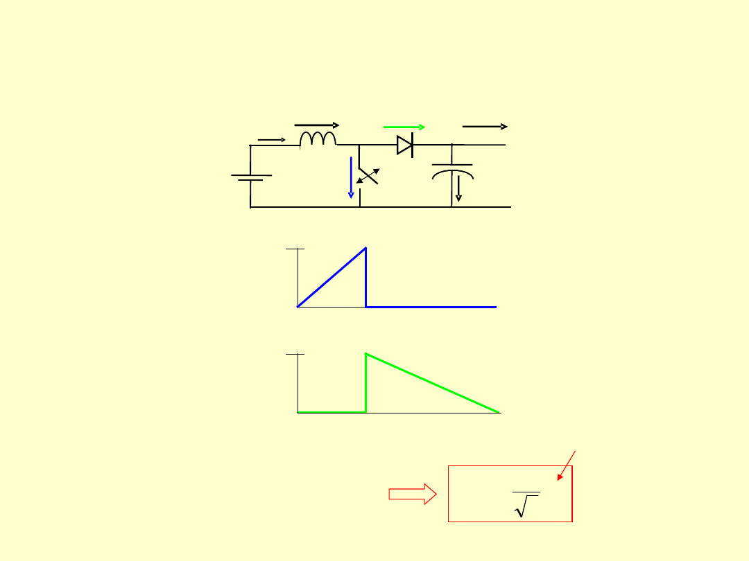
Boost converter
This is a much more unforgiving circuit than the buck
converter
V
in
+
V
out
–
C
i
C
I
out
i
in
i
L
L
+ v
L
–
i
D
•If the MOSFET gate driver sticks in the “on” position,
then there is a short circuit through the MOSFET –
blow
MOSFET!
•If the load is disconnected during operation, so that I
out
= 0, then L continues to push power to the right and
very quickly charges C up to a high value (250V) –
blow diode and MOSFET!
•Before applying power, make sure that your D is at the
minimum, and that a load is solidly connected
!
4
Boost converter
V
in
+
V
out
–
C
i
C
I
out
i
in
i
L
L
+ v
L
–
i
D
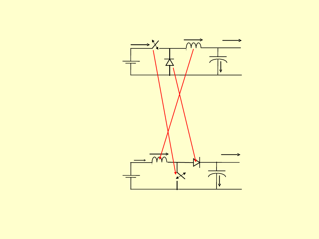
•Modify your MOSFET firing circuit for Boost
Converter operation (see the MOSFET Firing Circuit
document)
•Limit your output voltage to 120V
5
Boost converter
Using KVL and KCL in the average sense, the
average values are
+ 0 V –
I
out
V
in
+
V
out
–
C
I
out
L
0 A
I
in
V
in
+
V
out
–
C
i
C
I
out
i
in
i
L
L
+ v
L
–
i
D
Find the input/output equation by examining the
voltage across the inductor
6
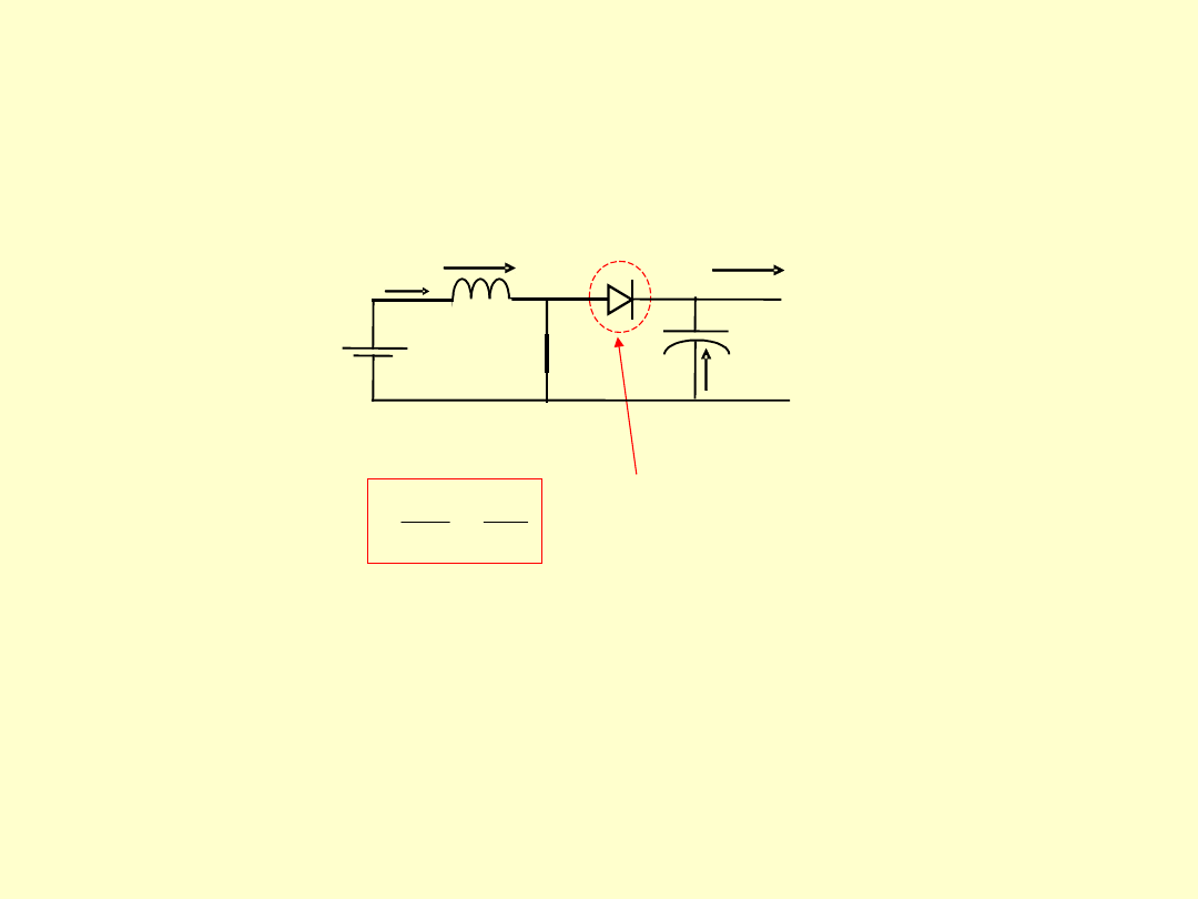
Switch closed for DT seconds
Reverse biased, thus the
diode is open
L
V
dt
di
in
L
for DT
seconds
V
in
+
V
out
–
C
I
out
i
in
i
L
L
I
out
Note – if the switch stays closed, the input is short circuited!
+ V
in
−
7
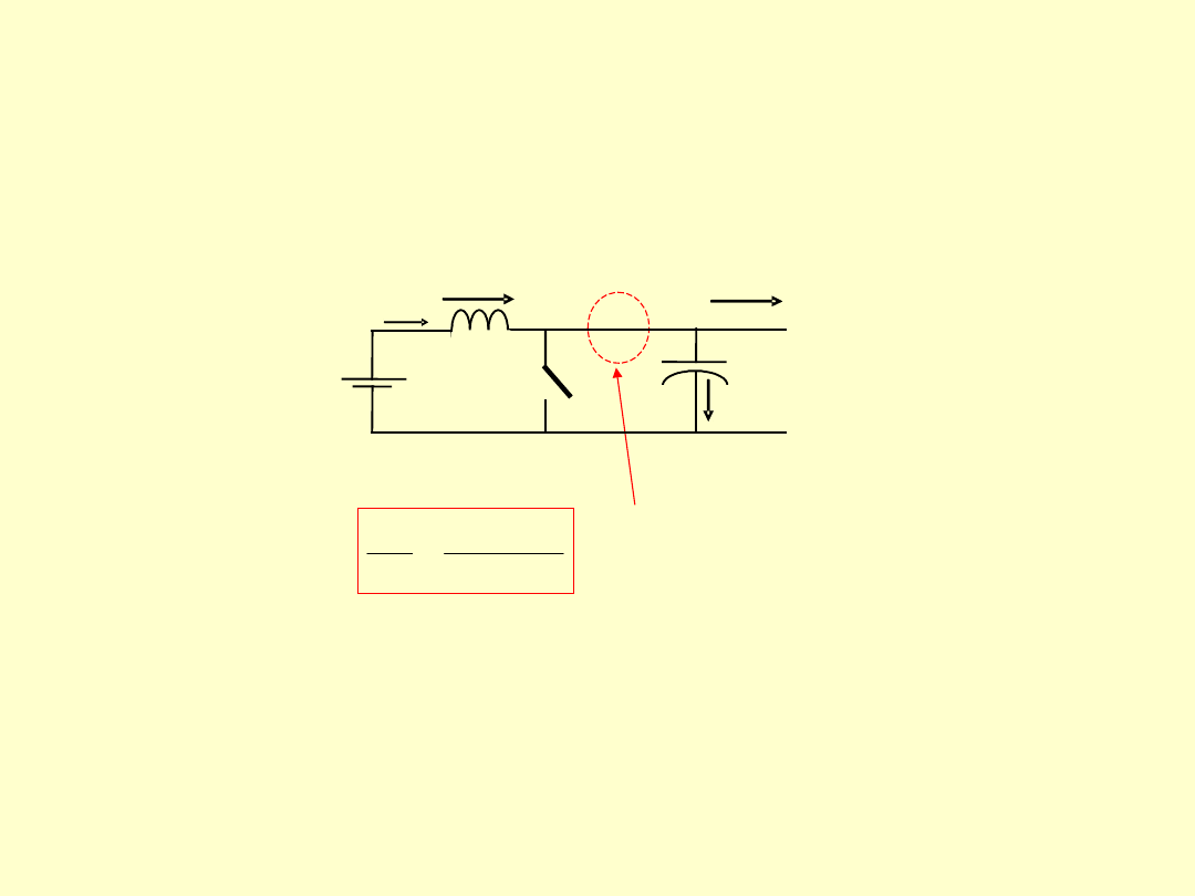
Switch open for (1 − D)T seconds
Diode closed. Assume
continuous conduction.
L
V
V
dt
di
out
in
L
V
in
+
V
out
–
C
I
out
i
in
i
L
L
for (1−D)T seconds
(i
L
– I
out
)
+ (V
in
− V
out
)
−

8
Since the average voltage across L is
zero
0
1
out
in
in
Lavg
V
V
D
V
D
V
in
in
in
out
V
D
V
D
V
D
V
)
1
(
D
V
V
in
out
1
The input/output equation
becomes
A realistic upper limit on boost is 5
times
!
9
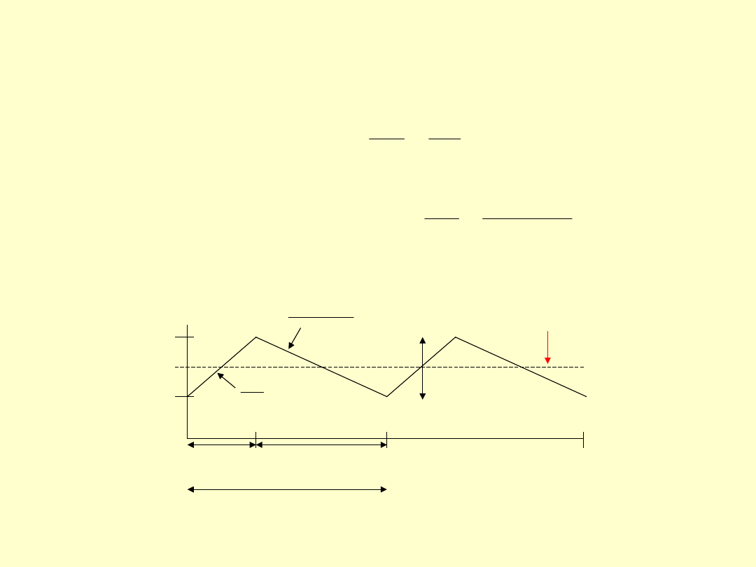
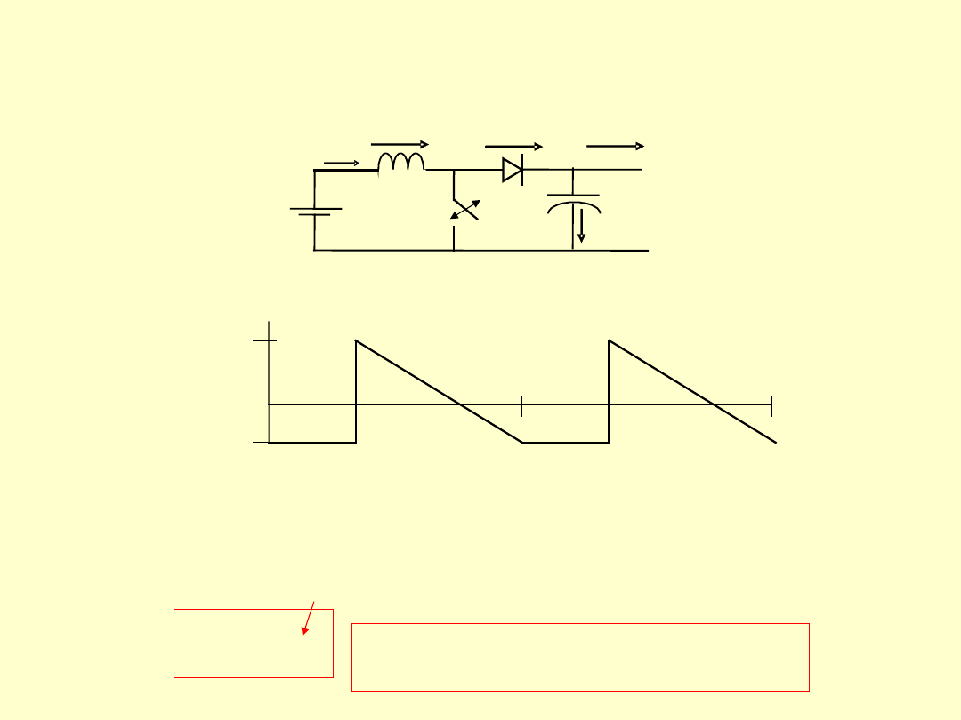
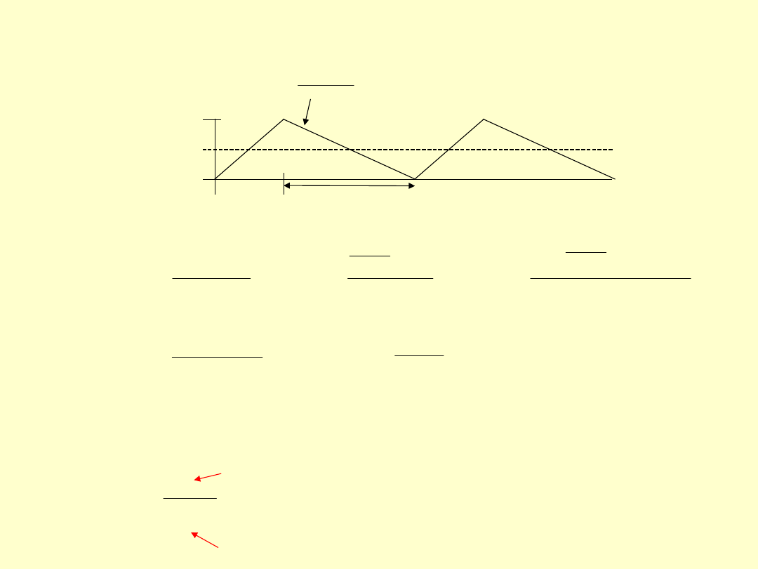
Examine the inductor current
Switch
closed,
Switch open,
L
V
dt
di
V
v
in
L
in
L
,
L
V
V
dt
di
V
V
v
out
in
L
out
in
L
,
sec
/
A
L
V
in
DT
(1 − D)T
T
I
max
I
min
I
avg
= I
in
I
avg
= I
in
is half way between
I
max
and I
min
sec
/
A
L
V
V
out
in
ΔI
i
L
10
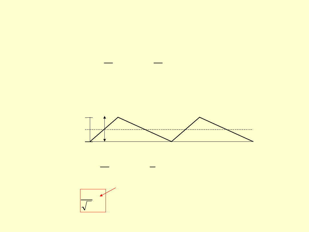
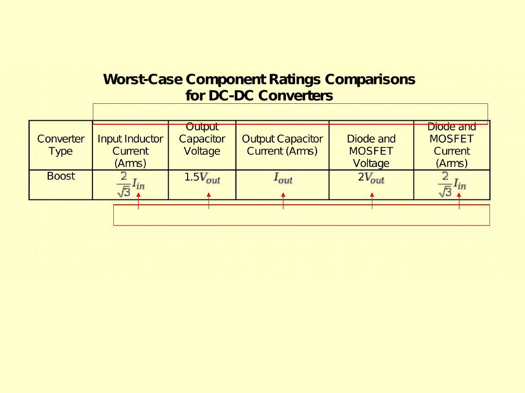
Inductor current rating
2
2
2
2
2
12
1
12
1
I
I
I
I
I
in
pp
avg
Lrms
2
2
2
2
3
4
2
12
1
in
in
in
Lrms
I
I
I
I
Max impact of ΔI on the rms current occurs at the boundary of
continuous/discontinuous conduction, where ΔI =2I
in
in
Lrms
I
I
3
2
2I
in
0
I
avg
= I
in
ΔI
i
L
Use max
11
MOSFET and diode currents and current
ratings
in
rms
I
I
3
2
Use max
2I
in
0
2I
in
0
Take worst case D for
each
V
in
+
V
out
–
C
i
C
I
out
i
in
i
L
L
+ v
L
–
i
D
12
Capacitor current and current rating
2I
in
−I
out
−I
out
0
Max rms current occurs at the boundary of
continuous/discontinuous conduction, where ΔI =2I
out
out
Crms
I
I
Use
max
i
C
= (i
D
– I
out
)
V
in
+
V
out
–
C
i
C
I
out
i
in
i
L
L
i
D
See the lab document for the
derivation
13
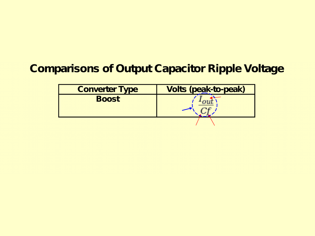
Worst-case load ripple voltage
Cf
I
C
T
I
C
Q
V
out
out
The worst case is where C provides I
out
for most of the period.
Then,
−I
out
0
i
C
= (i
D
– I
out
)
14
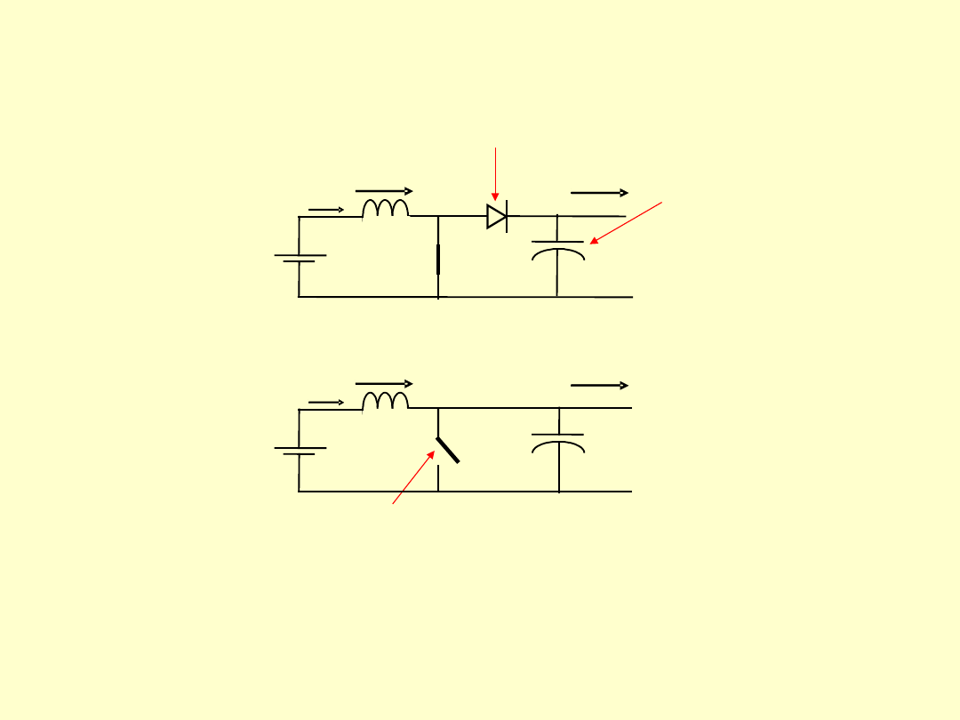
Voltage ratings
Diode sees V
out
MOSFET sees V
out
C sees V
out
• Diode and MOSFET, use 2V
out
• Capacitor, use 1.5V
out
V
in
+
V
out
–
C
I
out
i
in
i
L
L
V
in
+
V
out
–
C
I
out
i
in
i
L
L
15
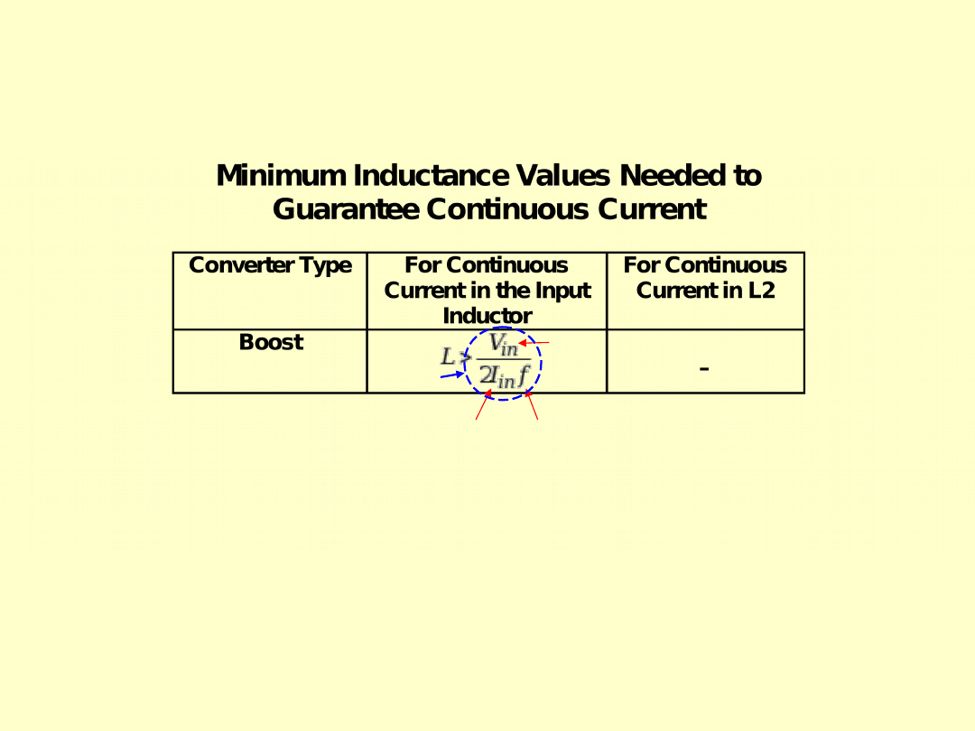
Continuous current in L
sec
/
A
L
V
V
out
in
f
L
D
D
V
T
D
L
V
D
V
T
D
L
V
V
I
boundary
in
boundary
in
in
boundary
in
out
in
1
1
1
1
1
1
1
2
f
I
D
V
L
in
in
boundary
2
2I
in
0
I
avg
= I
in
i
L
(1 − D)T
f
I
V
L
in
in
2
guarantees continuous
conduction
Then, considering the worst case (i.e., D → 1),
use max
use min
,
2
f
L
D
V
I
boundary
in
in
16
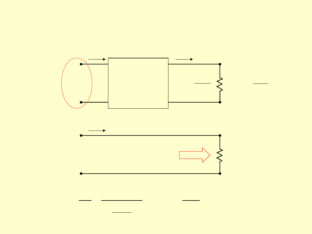
Impedance matching
out
out
load
I
V
R
equiv
R
load
out
out
out
out
in
in
equiv
R
D
I
V
D
D
I
V
D
I
V
R
2
2
1
1
1
1
DC−DC Boost
Converter
+
V
in
−
+
−
I
in
+
V
in
−
I
in
Equivalent from
source perspective
Source
D
V
V
in
out
1
in
out
I
D
I
1
17
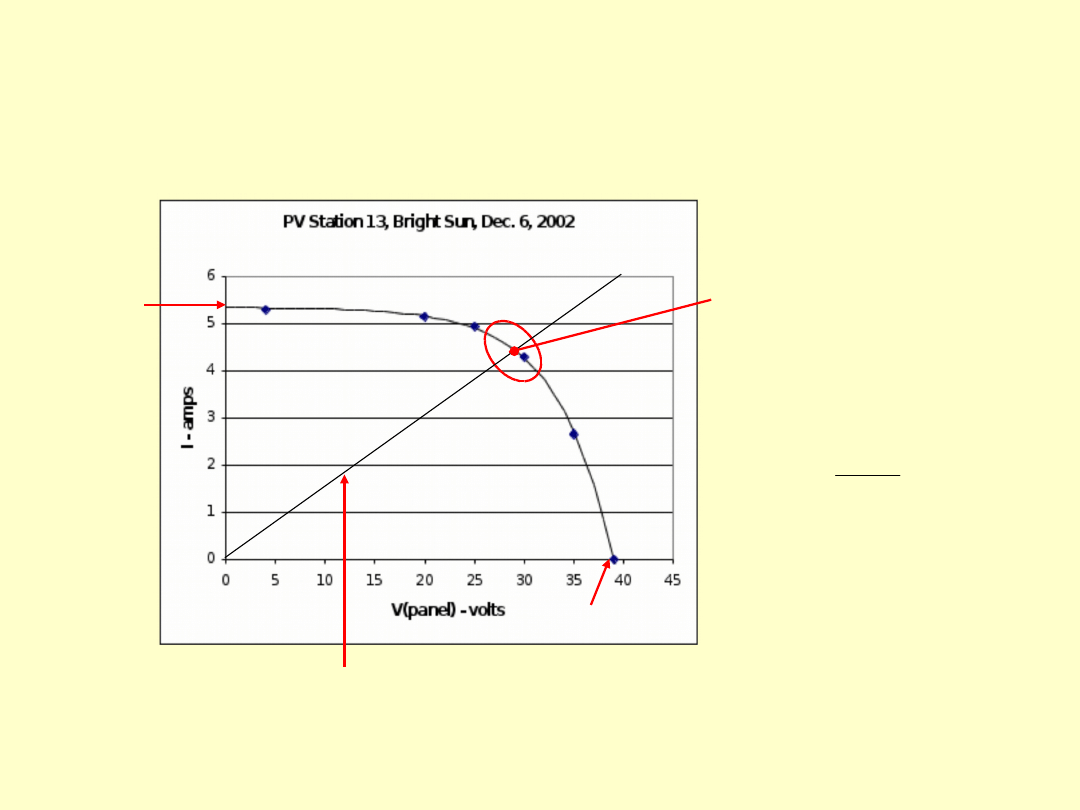
Example of drawing maximum power
from solar panel
I
sc
V
oc
P
max
is approx.
130W (occurs at
29V, 4.5A)
44
.
6
5
.
4
29
A
V
R
load
For max power from
panels, attach
I-V characteristic of 6.44Ω
resistor
But as the sun
conditions change,
the “max power
resistance” must also
change
18
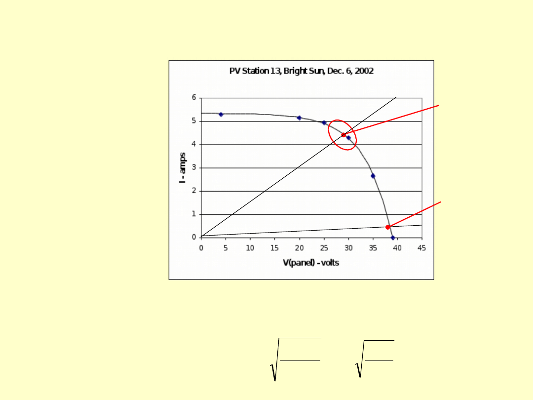
Connect a 100Ω resistor directly, extract only
14W
130W
6.4
4Ω
res
ist
or
100Ω
resistor
14W
75
.
0
100
44
.
6
1
1
,
1
2
load
equiv
load
equiv
R
R
D
R
D
R
To extract maximum power (130W), connect a boost converter
between the panel and the load resistor, and use D to modify the
equivalent load resistance seen by the source so that maximum
power is transferred
So, the boost
converter reflects a
high load resistance
to a low resistance
on the source side
19
5A
10A
10A
120V
120V
Likely worst-case boost situation
5.66A
200V,
250V
16A, 20A
Our components
9A
250V
MOSFET. 250V, 20A
L. 100µH,
9A
C. 1500µF, 250V, 5.66A
p-p
Diode. 200V, 16A
BOOST DESIGN
20
5A
1500µF50kHz
0.067V
BOOST DESIGN
MOSFET. 250V, 20A
L. 100µH,
9A
C. 1500µF, 250V, 5.66A
p-p
Diode. 200V, 16A
21
40V
2A
50kHz
200µH
BOOST DESIGN
MOSFET. 250V, 20A
L. 100µH,
9A
C. 1500µF, 250V, 5.66A
p-p
Diode. 200V, 16A
Document Outline
- EE462L, Spring 2014 DC−DC Boost Converter
- PowerPoint Presentation
- Slide 3
- Slide 4
- Slide 5
- Slide 6
- Slide 7
- Since the average voltage across L is zero
- Slide 9
- Inductor current rating
- MOSFET and diode currents and current ratings
- Capacitor current and current rating
- Worst-case load ripple voltage
- Slide 14
- Continuous current in L
- Impedance matching
- Example of drawing maximum power from solar panel
- Connect a 100Ω resistor directly, extract only 14W
- Slide 19
- Slide 20
- Slide 21
Wyszukiwarka
Podobne podstrony:
DC DC Converters k99e25 l1120
Boost Converter Design For 20Kw Wind Turbine Generator
IFL90 ch4 DC DC Converter intel
Inverter DC DC Converter Inductorless
Development Of High Frequency Link Direct Dc To Ac Converters For Link Direct Dc To Ac Converters Fo
DC DC Converter for EWB Wind Turbine Project review
inverter 2002 chapter 4 DC to AC conversion inverter tutorial
M Dąbrowska Kobieta piękną jest
drzwi czech e60 EASY 719 DC RC
2006 03 Sterowanie PWM silnikami DC większej mocy
stale, Elektrotechnika, dc pobierane, Podstawy Nauk o materialach, Przydatne, Sprawka
06, Szkoła, Politechnika 1- 5 sem, chomikuj, 4 sem (graviora), dc word (graviora)
dc dc stepup, Schematic Prints
Przetwornica DC DC (AVT1507)
Przeksztaltniki DC DC Prezentacja Kawy
dc valentines heart
ściąga z fizyki, dc, GPF, Fizyka lab, Ściągi, sciąga z fizyki
więcej podobnych podstron