
GENERAL
Page
Quality
2
Pro Electron type numbering system
2
Rating systems
3
Letter symbols
4
S-parameter definitions
7
Equivalent package designators
8
Transistor ratings
8
Thermal considerations
11
Power derating curves for SMDs
15
Power derating curve for SOT23
15
Power derating curve for SOT143
15
Power derating curve for SC-59
15
Power derating curve for SC-70
15
Power derating curve for SC-88
16
Power derating curve for SC-75
16
Power derating curves for SOT89
16
Power derating curves for SOT223
18
Thermal impedance curves
20
Thermal impedance curves for SOT23
20
Thermal impedance curves for SOT143
20
Thermal impedance curves for SC-59
21
Thermal impedance curves for SC-70
21
Thermal impedance curves for SC-88
22
Thermal impedance curves for SC-75
22
Thermal impedance curves for SOT89
23
Thermal impedance curves for SOT223
25
Thermal impedance curves for SOT54
27
Thermal impedance curves for TO-126
28
Thermal impedance curves for TO-202
30
Tape and reel packing
See SC18 “Package Databook” for detailed information.
Mounting and soldering
See SC18 “Package Databook” for detailed information.

1997 Aug 20
2
Philips Semiconductors
Small-signal Transistors
General
QUALITY
Total Quality Management
Philips Semiconductors is a Quality Company, renowned
for the high quality of our products and service. We keep
alive this tradition by constantly aiming towards one
ultimate standard, that of zero defects. This aim is guided
by our Total Quality Management (TQM) system which is
described in our Quality manuals. The basis is outlined in
the following paragraphs.
Q
UALITY ASSURANCE
Based on ISO 9000 standards, customer standards such
as FDC, QS 9000 and IBM MDQ. Our factories are
certified to ISO 9000 by external inspectorates.
P
ARTNERSHIPS WITH CUSTOMERS
PPM co-operations, design-in agreements, ship-to-stock,
just-in-time and self-qualification programmes, and
application support.
P
ARTNERSHIPS WITH SUPPLIERS
Ship-to-stock, statistical process control and ISO 9000
audits.
Q
UALITY IMPROVEMENT PROGRAMME
Continuous process and system improvement, design
improvement, complete use of statistical process control,
realization of our final objective of zero defects, and
logistics improvement by ship-to-stock and just-in-time
agreements.
Advanced quality planning
During the design and development of new products and
processes, quality is built-in by advanced quality planning.
Through failure-mode-and-effect analysis the critical
process parameters are detected and measures taken to
ensure good performance on these parameters. The
capability of process steps is also planned in this phase in
preparation for production under statistical process
control.
Product conformance
The assurance of product conformance is an integral part
of our Quality Assurance (QA) practice. This is achieved
by:
•
Incoming material control through partnerships with
suppliers.
•
In-line quality assurance to monitor process
reproducibility during manufacture and initiate any
necessary corrective action. Process steps are under
statistical process control.
•
Acceptance tests on finished products to verify
conformance with the device specification. The test
results are used for quality feedback and corrective
actions. The inspection and test requirements are
detailed in the general quality specifications
SNW-EQ-611 part A.
•
Periodic inspections to monitor and measure the
conformance of products (see SNW-EQ-611 part A).
•
Qualification tests (see SNW-EQ-611 part A).
Product reliability
With the increasing complexity of Original Equipment
Manufacturer (OEM) equipment, component reliability
must be extremely high. Our research laboratories and
development departments study the failure mechanisms of
semiconductors. Their studies result in design rules and
process optimization for the highest built-in product
reliability. Highly accelerated tests are applied to the
product’s reliability evaluation. Rejects from reliability tests
and from customer complaints are submitted to failure
analysis, to result in corrective action.
Customer response
Our quality improvement depends on working together
with our customer. We need our customer’s inputs and we
invite constructive comments on all aspects of our
performance. Please contact our local sales
representative.
PRO ELECTRON TYPE NUMBERING SYSTEM
Basic type number
This type designation code applies to discrete
semiconductor devices (not integrated circuits), multiples
of such devices, semiconductor chips and Darlington
transistors.
F
IRST LETTER
The first letter gives information about the material for the
active part of the device.
A
Germanium or other material with a band gap of
0.6 to 1 eV
B
Silicon or other material with a band gap of
1 to 1.3 eV

1997 Aug 20
3
Philips Semiconductors
Small-signal Transistors
General
C
Gallium arsenide (GaAs) or other material with a
band gap of 1.3 eV or more
R
Compound materials, e.g. cadmium sulphide.
S
ECOND LETTER
The second letter indicates the function for which the
device is primarily designed. The same letter can be used
for multi-chip devices with similar elements.
In the following list low power types are defined by
R
th j-mb
> 15 K/W and power types by R
th j-mb
≤
15 K/W.
A
Diode; signal, low power
B
Diode; variable capacitance
C
Transistor; low power, audio frequency
D
Transistor; power, audio frequency
E
Diode; tunnel
F
Transistor; low power, high frequency
G
Multiple of dissimilar devices/miscellaneous
devices; e.g. oscillators. Also with special third
letter; see under Section “Serial number”.
H
Diode; magnetic sensitive
L
Transistor; power, high frequency
N
Photocoupler
P
Radiation detector; e.g. high sensitivity
photo-transistor; with special third letter
Q
Radiation generator; e.g. LED, laser; with special
third letter
R
Control or switching device; e.g. thyristor, low
power; with special third letter
S
Transistor; low power, switching
T
Control or switching device; e.g. thyristor, power;
with special third letter
U
Transistor; power, switching
W
Surface acoustic wave device
X
Diode; multiplier, e.g. varactor, step recovery
Y
Diode; rectifying, booster
Z
Diode; voltage reference or regulator, transient
suppressor diode; with special third letter.
S
ERIAL NUMBER
The number comprises three figures running from
100 to 999 for devices primarily intended for consumer
equipment, or one letter (Z, Y, X, etc.) and two figures
running from 10 to 99 for devices primarily intended for
industrial or professional equipment.
(1)
Version letter
A letter may be added to the basic type number to indicate
minor electrical or mechanical variants of the basic type.
RATING SYSTEMS
The rating systems described are those recommended by
the IEC in its publication number 134.
Definitions of terms used
E
LECTRONIC DEVICE
An electronic tube or valve, transistor or other
semiconductor device. This definition excludes inductors,
capacitors, resistors and similar components.
C
HARACTERISTIC
A characteristic is an inherent and measurable property of
a device. Such a property may be electrical, mechanical,
thermal, hydraulic, electro-magnetic or nuclear, and can
be expressed as a value for stated or recognized
conditions. A characteristic may also be a set of related
values, usually shown in graphical form.
B
OGEY ELECTRONIC DEVICE
An electronic device whose characteristics have the
published nominal values for the type. A bogey electronic
device for any particular application can be obtained by
considering only those characteristics that are directly
related to the application.
R
ATING
A value that establishes either a limiting capability or a
limiting condition for an electronic device. It is determined
for specified values of environment and operation, and
may be stated in any suitable terms. Limiting conditions
may be either maxima or minima.
R
ATING SYSTEM
The set of principles upon which ratings are established
and which determine their interpretation. The rating
system indicates the division of responsibility between the
device manufacturer and the circuit designer, with the
object of ensuring that the working conditions do not
exceed the ratings.
(1) When the supply of these serial numbers is exhausted, the
serial number may be expanded to three figures for industrial
types and four figures for consumer types.

1997 Aug 20
4
Philips Semiconductors
Small-signal Transistors
General
Absolute maximum rating system
Absolute maximum ratings are limiting values of operating
and environmental conditions applicable to any electronic
device of a specified type, as defined by its published data,
which should not be exceeded under the worst probable
conditions.
These values are chosen by the device manufacturer to
provide acceptable serviceability of the device, taking no
responsibility for equipment variations, environmental
variations, and the effects of changes in operating
conditions due to variations in the characteristics of the
device under consideration and of all other electronic
devices in the equipment.
The equipment manufacturer should design so that,
initially and throughout the life of the device, no absolute
maximum value for the intended service is exceeded with
any device, under the worst probable operating conditions
with respect to supply voltage variation, equipment
component variation, equipment control adjustment, load
variations, signal variation, environmental conditions, and
variations in characteristics of the device under
consideration and of all other electronic devices in the
equipment.
Design maximum rating system
Design maximum ratings are limiting values of operating
and environmental conditions applicable to a bogey
electronic device of a specified type as defined by its
published data, and should not be exceeded under the
worst probable conditions.
These values are chosen by the device manufacturer to
provide acceptable serviceability of the device, taking
responsibility for the effects of changes in operating
conditions due to variations in the characteristics of the
electronic device under consideration.
The equipment manufacturer should design so that,
initially and throughout the life of the device, no design
maximum value for the intended service is exceeded with
a bogey electronic device, under the worst probable
operating conditions with respect to supply voltage
variation, equipment component variation, variation in
characteristics of all other devices in the equipment,
equipment control adjustment, load variation, signal
variation and environmental conditions.
Design centre rating system
Design centre ratings are limiting values of operating and
environmental conditions applicable to a bogey electronic
device of a specified type as defined by its published data,
and should not be exceeded under normal conditions.
These values are chosen by the device manufacturer to
provide acceptable serviceability of the device in average
applications, taking responsibility for normal changes in
operating conditions due to rated supply voltage variation,
equipment component variation, equipment control
adjustment, load variation, signal variation, environmental
conditions, and variations in the characteristics of all
electronic devices.
The equipment manufacturer should design so that,
initially, no design centre value for the intended service is
exceeded with a bogey electronic device in equipment
operating at the stated normal supply voltage.
LETTER SYMBOLS
The letter symbols for transistors detailed in this section
are based on IEC publication number 148.
Letter symbols for currents, voltages and powers
B
ASIC LETTERS
I, i
current
V, v
voltage
P, p
power.
Upper-case letter symbols are used to represent all values
except instantaneous values that vary with time, these are
represented by lower-case letters.
S
UBSCRIPTS
A, a
anode terminal
(AV), (av)
average value
B, b
base terminal
C, c
collector terminal
D, d
drain terminal
E, e
emitter terminal
F, f
forward
G, g
gate terminal
K, k
cathode terminal
M, m
peak value
O, o
as third subscript: the terminal not
mentioned is open-circuit
R, r
as first subscript: reverse. As second
subscript: repetitive. As third subscript: with
a specified resistance between the terminal
not mentioned and the reference terminal

1997 Aug 20
5
Philips Semiconductors
Small-signal Transistors
General
(RMS), (rms) root-mean-square value
S, s
as first or second subscript: source terminal
(FETs only). As second subscript:
non-repetitive (not FETs). As third subscript:
short circuit between the terminal not
mentioned and the reference terminal
X, x
specified circuit
Z, z
replaces R to indicate the actual working
voltage, current or power of voltage
reference and voltage reference diodes.
No additional subscript is used for DC values.
Upper-case subscripts are used for the indication of:
•
Continuous (DC) values (without signal), e.g. I
B
•
Instantaneous total values, e.g. i
B
•
Average total values, e.g. I
B(AV)
•
Peak total values, e.g. I
BM
•
Root-mean-square total values, e.g. I
B(RMS)
.
Lower-case subscripts are used for the indication of values
applying to the varying component alone:
•
Instantaneous values, e.g. i
b
•
Root-mean-square values, e.g. I
b(rms)
•
Peak values, e.g. I
bm
•
Average values, e.g. I
b(av)
.
If more than one subscript is used, the subscript for which
both styles exist are either all upper-case or all lower-case.
A
DDITIONAL RULES FOR SUBSCRIPTS
Transistor currents
If it is necessary to indicate the terminal carrying the
current, this should be done by the first subscript
(conventional current flow from the external circuit into the
terminal is positive).
Examples: I
B
, i
B
, i
b
, I
bm
.
Transistor voltages
If it is necessary to indicate the points between which a
voltage is measured, this should be done by the first two
subscripts. The first subscript indicates the terminal at
which the voltage is measured and the second the
reference terminal or the circuit node. Where there is no
possibility of confusion, the second subscript may be
omitted.
Examples: V
BE
, v
BE
, v
be
, V
bem
.
Supply voltages or currents
Supply voltages or supply currents are indicated by
repeating the appropriate terminal subscript.
Examples: V
CC
, I
EE
.
If it is necessary to indicate a reference terminal, this
should be done by a third subscript.
Example: V
CCE
.
Subscripts for devices with more than one terminal of the
same kind
If a device has more than one terminal of the same kind,
the subscript is formed by the appropriate letter for the
terminal, followed by a number. In the case of multiple
subscripts, hyphens may be necessary to avoid confusion.
Examples:
I
B2
continuous (DC) current flowing into the second
base terminal
V
B2-E
continuous (DC) voltage between the terminals of
second base and emitter terminals.
Subscripts for multiple devices
For multiple unit devices, the subscripts are modified by a
number preceding the letter subscript. In the case of
multiple subscripts, hyphens may be necessary to avoid
confusion.
Examples:
I
2C
continuous (DC) current flowing into the collector
terminal of the second unit
V
1C-2C
continuous (DC) voltage between the collector
terminals of the first and second units.
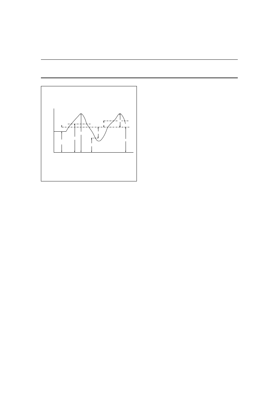
Application of the rules
Figure 1 represents a transistor collector current as a
function of time. It comprises a continuous (DC) current
and a varying component.
1997 Aug 20
6
Philips Semiconductors
Small-signal Transistors
General
Letter symbols for electrical parameters
D
EFINITION
For the purpose of this publication, the term ‘electrical
parameter’ applies to four-pole matrix parameters,
elements of electrical equivalent circuits, electrical
impedances and admittances, inductances and
capacitances.
B
ASIC LETTERS
The following list comprises the most important basic
letters used for electrical parameters of semiconductor
devices.
B, b
susceptance (imaginary part of an admittance)
C
capacitance
G, g
conductance (real part of an admittance)
H, h
hybrid parameter
L
inductance
R, r
resistance (real part of an impedance)
X, x
reactance (imaginary part of an impedance)
Y, y
admittance
Z, z
impedance.
Upper-case letters are used for the representation of:
•
Electrical parameters of external circuits and of circuits
in which the device forms only a part
•
All inductances and capacitances.
Fig.1 Collector current as a function of time.
MBD537
collector
current
0
I C
(no signal)
I C(RMS)
I c(av)
I CM
i c
i c
I c(rms)
I cm
I C(AV)
time
Lower-case letters are used for the representation of
electrical parameters inherent in the device, with the
exception of inductances and capacitances.
S
UBSCRIPTS
General subscripts
The following list comprises the most important general
subscripts used for electrical parameters of semiconductor
devices.
F, f
forward (forward transfer)
I, i (or 1)
input
L, l
load
O, o (or 2)
output
R, r
reverse (reverse transfer)
S, s
source.
Examples: Z
s
, h
f
, h
F
.
The upper-case variant of a subscript is used for the
designation of static (DC) values.
Examples:
h
FE
static value of forward current transfer ratio in
common-emitter configuration (DC current gain)
R
E
DC value of the external emitter resistance.
The static value is the slope of the line from the origin to
the operating point on the appropriate characteristic curve,
i.e. the quotient of the appropriate electrical quantities at
the operating point.
The lower-case variant of a subscript is used for the
designation of small-signal values.
Examples:
h
fe
small-signal value of the short-circuit
forward current transfer ratio in
common-emitter configuration
Z
e
= R
e
+ jX
e
small-signal value of the external
impedance.
If more than one subscript is used, subscripts for which
both styles exist are either all upper-case or all lower-case.
Examples: h
FE
, y
RE
, h
fe
.
Subscripts for four-pole matrix parameters
The first letter subscript (or double numeric subscript)
indicates input, output, forward transfer or reverse
transfer.
Examples: h
i
(or h
11
), h
o
(or h
22
), h
f
(or h
21
), h
r
(or h
12
).
1997 Aug 20
7
Philips Semiconductors
Small-signal Transistors
General
A further subscript is used for the identification of the circuit
configuration. When no confusion is possible, this further
subscript may be omitted.
Examples: h
fe
(or h
21e
), h
FE
(or h
21E
).
D
ISTINCTION BETWEEN REAL AND IMAGINARY PARTS
If it is necessary to distinguish between real and imaginary
parts of electrical parameters, no additional subscripts
should be used. If basic symbols for the real and imaginary
parts exist, these may be used.
Examples: Z
i
= R
i
+ jX
i
, y
fe
= g
fe
+ jb
fe
.
If such symbols do not exist, or if they are not suitable, the
following notation is used:
Examples:
Re (h
ib
) etc. for the real part of h
ib
Im (h
ib
) etc. for the imaginary part of h
ib
.
S-PARAMETER DEFINITIONS
S-parameters S
11
and S
22
(return losses)
In accordance with IEC 747-7.
D
EFINITION
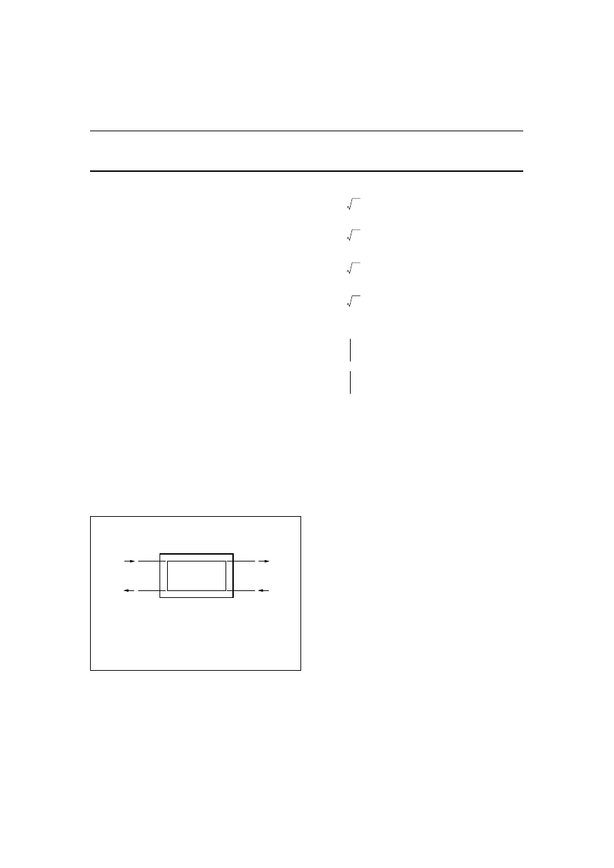
The return losses or reflection coefficients of a module can
be defined as the S
11
and the S
22
of a two-port network
(see Fig.2).
(1)
(2)
where:
Fig.2
Two-port network with reflection coefficients
S
11
and S
22
.
D.U.T.
S11
S 22
a 1
b 1
b 2
a 2
MLB335
b
1
S
11
a
1
S
12
a
2
⋅
+
⋅
=
b
2
S
21
a
1
S
22
a
2
⋅
+
⋅
=
(3)
(4)
From (1) and (2) formulae for the return losses can be
derived:
(5)
(6)
In (5), a
2
= 0 means output port terminated with Z
0
(derived from formula (4)).
In (6), a
1
= 0 means input port terminated with Z
0
(derived from formula (3)).
M
EASUREMENT
The return losses are measured with a network analyzer
after calibration, where the influence of the test jig is
eliminated. The necessary termination of the other port
with Z
0
is done automatically by the network analyzer.
The network analyser must have a directivity of at least
40 dB to obtain an accuracy of 0.5 dB when measuring
return loss figures of 20 dB. A full two-port correction
method can be used to improve the accuracy.
Spice parameter data
Spice parameters are included with this data handbook on
floppy disks labelled “Philips simulation data selection
program for LF small-signal transistors”.
a
1
1
2
Z
0
⋅
------------------
V
1
Z
0
i
1
⋅
+
(
)
⋅
signal into port 1
=
=
a
2
1
2
Z
0
⋅
------------------
V
2
Z
0
i
2
⋅
+
(
)
⋅
signal into port 2
=
=
b
1
1
2
Z
0
⋅
------------------
V
1
Z
0
i
1
⋅
+
(
)
⋅
signal out of port 1
=
=
b
2
1
2
Z
0
⋅
------------------
V
2
Z
0
i
2
⋅
+
(
)
⋅
signal out of port 2
=
=
S
11
b
1
a
1
------ a
2
0
=
=
S
22
b
2
a
2
------ a
1
0
=
=

1997 Aug 20
8
Philips Semiconductors
Small-signal Transistors
General
EQUIVALENT PACKAGE DESIGNATORS
TRANSISTOR RATINGS
Voltage ratings
C
OLLECTOR TO BASE
V
CBmax
The maximum permissible instantaneous
voltage between collector and base
terminals. The collector voltage is negative
with respect to base in pnp transistors and
positive with respect to base in npn types.
V
CBmax
(I
E
= 0)
The maximum permissible instantaneous
voltage between collector and base
terminals when the emitter terminal is
open-circuit.
E
MITTER TO BASE
V
EBmax
The maximum permissible instantaneous
voltage between emitter and base terminals.
The emitter voltage is negative with respect
to base in pnp transistors and positive with
respect to base in npn types.
V
EBmax
(I
C
= 0)
The maximum permissible instantaneous
voltage between emitter and base terminals
when the collector terminal is open-circuit.
C
OLLECTOR TO EMITTER
V
CEmax
The maximum permissible instantaneous
voltage between collector and emitter
terminals. The collector voltage is negative
with respect to emitter in pnp transistors and
positive with respect to emitter in npn types.
This rating is very dependent on circuit
Philips
designator
Industry
designator
Philips
designator
Industry
designator
Leaded metal can
Surface-mount plastic
SOT5/11
TO-39
SOT23
SOT23
SOT18/9
TO-72
SOT89
SOT89
SOT18/13
TO-18
SOT143
SOT143
SOT31
TO-71
SOT223
SOT223
Leaded plastic
SOT323
SC-70
SOT32
TO-126
SOT346
SC-59
SOT54
TO-92
SOT363
SC-88
SOT128
TO-202
SOT416
SC-75
conditions and collector current, and it is
necessary to refer to the curve of V
CE
versus
I
C
for the appropriate circuit condition in
order to obtain the correct rating.
V
CEmax
(Cut-off)
The maximum permissible instantaneous
voltage between collector and emitter
terminals when the emitter current is
reduced to zero by means of a reverse
emitter base voltage, i.e. the base voltage is
normally positive with respect to emitter for
pnp transistors and negative with respect to
emitter for npn types. The term ‘(Cut-off)’ is
sometimes replaced by V
BE
> x V, or
R
B
/R
E
≤
y, which are equivalent conditions
under which the transistor may be cut off.
V
CEmax
(I
C
= x mA)
The maximum permissible instantaneous
voltage between collector and emitter
terminals when the collector current is at a
high value, often the maximum rated value.
V
CEmax
(I
B
= 0)
The maximum permissible instantaneous
voltage between collector and emitter
terminals when the base terminal is
open-circuit or when a very high resistance
is in series with the base terminal. Special
care must be taken to ensure that thermal
runaway due to excessive collector leakage
current does not occur in this condition.
Due to the current dependency of V
CE
it is usual to present
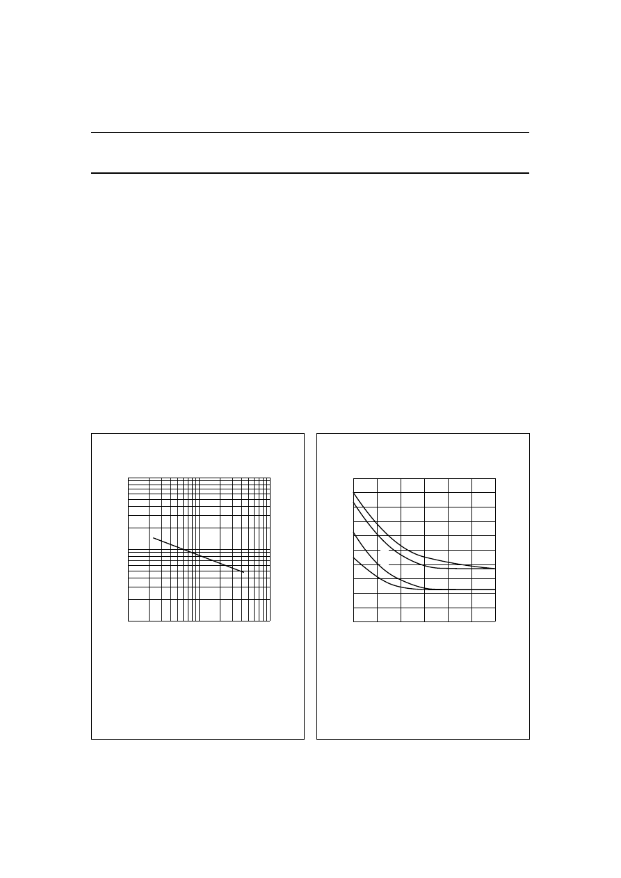
this information as a voltage rating chart, a curve of
collector current as a function of collector-to-emitter
voltage (see Fig.3). The permissible area of operation
under all conditions of base drive (provided the dissipation
rating is not exceeded) is shown as area 1 and operation
under certain specified conditions is shown as area 2.
To assist in determining the rating in area 2, further curves
can relate the voltage rating to external circuit conditions,
for example: R
B
/R
E
, R
B
, Z
Bg
,V
BE
, I
B
or V
BB
/R
B
. An example
of this type of curve is given in Fig.4 with V
CE
as a function
of R
B
/R
E
for two values of collector current.
It should be noted that when R
E
is shunted by a capacitor,
during switching, the collector voltage V
CE
must be
restricted to a value that does not rely on the effect of R
E
.
In the case of an inductive load, when an energy rating is
given, it may be safe to operate outside the rated area
provided the specified energy rating is not exceeded.
1997 Aug 20
9
Philips Semiconductors
Small-signal Transistors
General
Current ratings
C
OLLECTOR
I
Cmax
The maximum permissible collector current.
Without further qualification, the DC value is
implied.
I
C(AV)max
The maximum permissible average value of
the total collector current.
I
CM
The maximum permissible instantaneous
value of the total collector current.
Emitter
I
Emax
The maximum permissible emitter current.
Without further qualification, the DC value is
implied.
I
E(AV)max
The maximum permissible average value of
the total emitter current.
Fig.3 Graph of permissible operating areas.
handbook, halfpage
MBE247
VCE
area 1
area 2
I C
Fig.4
Graph showing effect of collector current on
permissible operating areas.
handbook, halfpage
MBE246
R /R
B
E
I = 0
C
I = I
C
Cmax
VCE
I
ER(AV)max
The maximum permissible average value of
the total emitter current when operating in the
reverse emitter-base breakdown region.
I
EM
The maximum permissible instantaneous
value of the total emitter current.
I
ERM
The maximum permissible instantaneous
value of the total emitter current when
operating in the reverse breakdown region.
B
ASE
I
Bmax
The maximum permissible base current.
Without further qualification, the DC value is
implied.
I
B(AV)max
The maximum permissible average value of
the total base current.
I
BR(AV)max
The maximum permissible average value of
the total base current when operating in the
reverse breakdown region.
I
BM
The maximum permissible instantaneous
value of the total base current. The rating also
includes the switch-off current.
I
BRM
The maximum permissible instantaneous
value of the total reverse current allowable in
the reverse breakdown region.
Power ratings
The total maximum permissible continuous power
dissipation in the transistor, P
tot max
, includes
collector-base dissipation and emitter-base dissipation.
Under steady state conditions, the total power is given as:
P
tot
= V
CE
×
I
C
+ V
BE
×
I
B
.
In order to distinguish between ‘steady state’ and ‘pulse’
conditions, the terms ‘steady state power (P
S
)’ and ‘pulse
power (P
P
)’ can be used. The permissible total power
dissipation is dependent on temperature; this relationship
is shown in Fig.5.
The temperature may be the ambient, the case or the
mounting base temperature. Where a cooling clip or
heatsink is attached to the device, the allowable power
dissipation is also dependent on the efficiency of the
heatsink.
The efficiency of this clip or heatsink is measured in terms
of its thermal resistance (R
th h
) normally expressed in
degrees Kelvin per Watt (K/W). For mounting-base rated
devices, the added effect of the contact resistance (R
th i
)
must be taken into account.

1997 Aug 20
10
Philips Semiconductors
Small-signal Transistors
General
The effect of heatsinks of various thermal and contact
resistance is often included in the graph of permissible
total power dissipation.
The relationship between maximum power dissipation,
ambient temperature and thermal heatsink resistance is
given by:
where R
th j-a
is the thermal resistance from the transistor
junction to the ambient. For case rated or mounting-base
rated devices, the thermal resistance R
th j
is made up of
the thermal resistance junction to case or mounting-base
(R
th j-mb
), the contact thermal resistance (R
th i
) and the
heatsink thermal resistance (R
th h
).
Fig.5 Permissible total power dissipation.
handbook, halfpage
MBE248
temperature
Ptot
P
tot
T
j
T
–
amb
R
th j a
–
---------------------
=
For the calculation of pulse power operation, the maximum
pulse power is obtained using a graph as shown in Fig.6
The general expression from which the maximum pulse
power dissipation can be calculated is:
where Z
th t
and
δ
are given in Fig.6 and R
th c
−
a
is the
thermal resistance between case and ambient for a case
rated device. For a mounting-base rated device, it is equal
to R
th h
+ R
th i
and is zero for a free-air rated device
because the effect of the temperature rise of the case over
the ambient for a pulse train is already included in Z
th t
.
Temperature ratings
T
j max
The maximum permissible junction temperature
which is used as the basis for the calculation of
power ratings. Unless otherwise stated, the
continuous value is implied.
T
j max
(continuous operation): indicates the
maximum permissible continuous value.
T
j max
(intermittent operation): indicates the
maximum permissible instantaneous junction
temperature usually allowed for a total duration of
200 hours.
T
mb
The temperature of the surface in contact with the
heatsink. This is confined to devices where a flange
or stud for fixing onto a heatsink forms an integral
part of the package.
T
case
The temperature of the package. This is confined to
devices that may have a clip-on cooling fin
attachment.
P
p
T
j
T
amb
P
S
–
R
th j a
–
×
–
Z
in t
d R
th c a
–
(
)
+
------------------------------------------------------------
=
Fig.6 Pulse power operation.
handbook, full pagewidth
MBE249
pulse width
δ
(duty factor) =
Zth t
T
t on
T
t on
1997 Aug 20
11
Philips Semiconductors
Small-signal Transistors
General
THERMAL CONSIDERATIONS
Thermal resistance
Circuit performance and long-term reliability are affected
by the temperature of the transistor die. Normally, both are
improved by keeping the die temperature (junction
temperature) low.
Electrical power dissipated in any semiconductor device is
a source of heat. This increases the temperature of the die
about some reference point, normally an ambient
temperature of 25
o
C in still air. The size of the increase in
temperature depends on the amount of power dissipated
in the circuit and the net thermal resistance between the
heat source and the reference point.
Devices lose most of their heat by conduction when
mounted on a printed board, a substrate or heatsink.
Referring to Fig.7 (for surface mounted devices mounted
on a substrate), heat conducts from its source (the
junction) via the package leads and soldered connections
to the substrate. Some heat radiates from the package into
the surrounding air where it is dispersed by convection or
by forced cooling air. Heat that radiates from the substrate
is dispersed in the same way.
The elements of thermal resistance shown in Fig.8 are
defined as follows:
R
th j-mb
thermal resistance from junction to mounting base
R
th j-c
thermal resistance from junction to case
R
th j-s
thermal resistance from junction to soldering point
R
th s-a
thermal resistance from soldering point to
ambient
R
th c-a
thermal resistance from case to ambient (R
th s-a
and R
th c-a
are the same for most packages)
R
th j-a
thermal resistance from junction to ambient.
Heat radiates from the package (1) to ambient.
Heat conducts via leads (2), solder joints (3) to the substrate (4).
Fig.7 Heat losses.
handbook, halfpage
,
,
,
MBB438
,
,
,,
,,
1
2
3
2
3
4
Fig.8
Representation of thermal resistance paths
of a device mounted on a substrate or
printed board.
handbook, halfpage
MBB439
R th j–s
ambient
junction
soldering
point or
case
R th j–a
R th c–a
R th j–mb R th j–c
=
1997 Aug 20
12
Philips Semiconductors
Small-signal Transistors
General
The temperature at the junction depends on the ability of
the package and its mounting to transfer heat from the
junction region to the ambient environment. The basic
relationship between junction temperature and power
dissipation is:
T
j max
= T
amb
+ P
tot max
(R
th j-s
+ R
th s-a
)
= T
amb
+ P
tot max
(R
th j-a
)
where
T
j max
is the maximum junction temperature
T
amb
is the ambient temperature
P
tot max
is the maximum power handling capability of the
device, including the effects of external loads
when applicable.
In the expression for T
j max
, only T
amb
and R
th s-a
can be
varied by the user. The package mounting technique and
the flow of cooling air are factors that affect R
th s-a
. The
device power dissipation can be controlled to a limited
extent but under recommended usage, the supply voltage
and circuit loading dictate a fixed power maximum. The
R
th j-s
value is essentially independent of external
mounting method and cooling air; but is sensitive to the
materials used in the package construction, the die
bonding method and the die area, all of which are fixed.
Values of T
j max
and R
th j-s
, or R
th j-c
or R
th j-a
are given in
the device data sheets. For applications where the
temperature of the case is stabilized by a large or
temperature-controlled heatsink, the junction temperature
can be calculated from:
T
j
= T
case
+ P
tot
×
R
th j-c
or, using the soldering point
definition, from T
j
= T
solder
+ P
tot
×
R
th j-s
.
R
th s-a
for SMDs
The thermal resistance R
th s-a
for SMDs mounted on a
ceramic substrate (Al
2
O
3
) is a function of the substrate
area as shown in Fig.9.
The thermal resistance R
th s-a
for SMDs mounted on a
printed circuit board (FR4) is a function of the board type
(single-sided or double-sided), track area and plated or
unplated tracks as shown in Fig.10.
Fig.9
Thermal resistance (R
th s-a
) as a function of
area of ceramic substrate.
handbook, halfpage
10
MBB447
1
10
10
3
10
2
10
−
1
area (cm )
2
Rth s-a
(K/W)
Fig.10 Thermal resistance (R
th s-a
) as a function of
copper area on different configurations of
FR4 epoxy fibre-glass circuit board.
(1) Single-sided, unplated.
(2) Single-sided, plated.
(3) Double-sided, unplated.
(4) Double-sided, plated.
handbook, halfpage
0
200
400
600
120
20
100
MBB446
80
60
40
pad area (mm
2
)
Rth s-a
(K/W)
(1)
(4)
(2)
(3)
1997 Aug 20
13
Philips Semiconductors
Small-signal Transistors
General
Temperature calculation under pulsed conditions
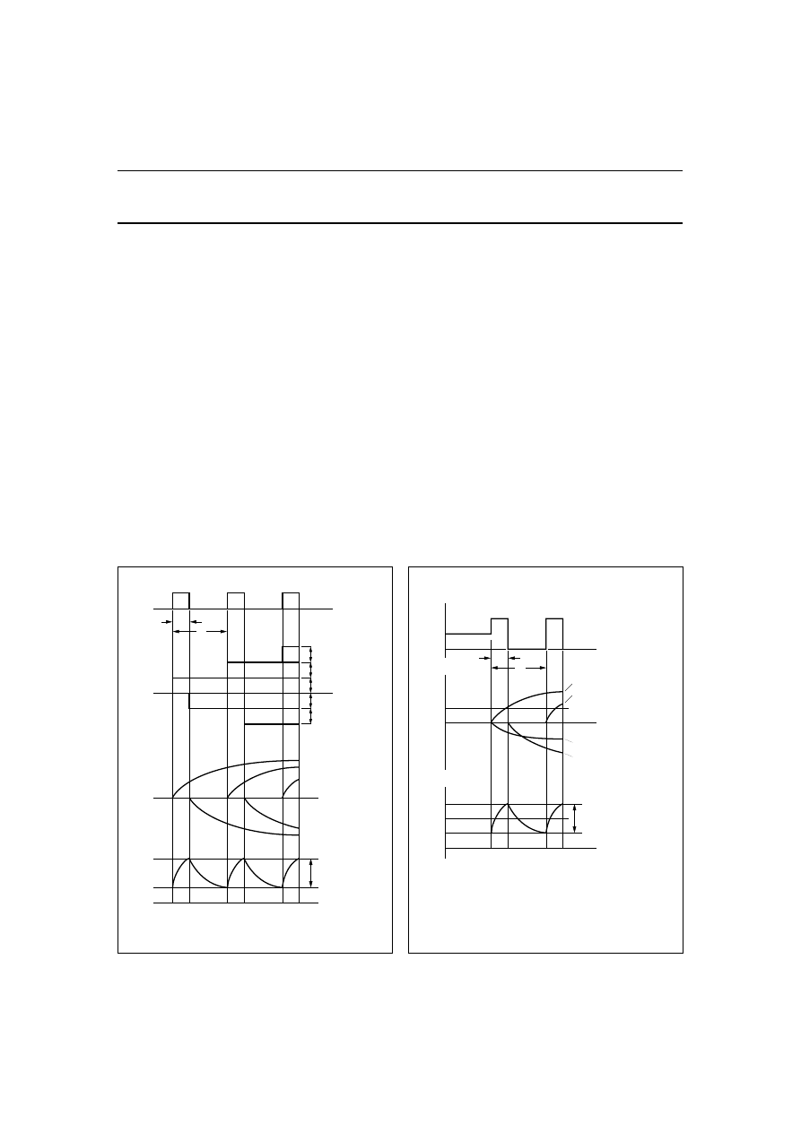
In pulsed power conditions, the peak temperature of
the die depends on the pulse time and duty factor as well
as the ability of the package and its mounting to disperse
heat.
When power is applied in repetitive square-wave pulses
with a certain duty factor (
δ
), the variation in junction
temperature has a sawtooth characteristic.
The average steady-state junction temperature is:
T
j(av)
= T
ref
+
δ ×
P
d
×
R
th j-ref
The peak junction temperature, however, is the most
relevant to performance reliability. This can be calculated
by heating and cooling step functions that result in heating
and cooling curves shifted in time as shown in Fig.11.
The peak value of T
j
is reached at the end of a power
pulse and the minimum value immediately before the next
power pulse. The thermal ripple is the difference between
T
j(peak)
and T
j(min)
.
Fig.11 Heating effect of three identical power
pulses after thermal stabilization.
handbook, halfpage
d
−
w/t
Pd (w)
power
+
0
Ta
−
∆
Tj
Tj
∆
T1
∆
T2
∆
T3
∆
T4
∆
T5
MBG391
Pd
Pd
Pd
Pd
Pd
Pd
t
w
Tj (peak)
thermal-ripple
Tj (min)
Calculation of T
j(peak)
after n pulses:
where a is an integer number.
Approximation method of finding T
j(peak)
With this method it is assumed that the average load is
immediately followed by two square power pulses as
shown in Fig.12. This two-pulse approximation method is
accurate enough for finding T
j(peak)
.
The junction temperature at the end of the second pulse is:
T
j(peak)
= T
ref
+ P
d
×
[
δ ×
R
th(j-ref)
+ (1
− δ
)
×
Z
th(t+w)
+ Z
th(w)
−
Z
th(t)
]
The junction temperature immediately before the second
power pulse is:
T
j(min)
= T
ref
+ P
d
×
[
δ ×
R
th(j-ref)
+ (1
− δ
)
×
Z
th(t)
−
Z
th(t
−
w)
]
T
j(peak)
T
ref
P
d
+
Z
th at
w
+
(
)
Z
th at
( )
–
[
]
a 0
=
a n
1
–
=
∑
×
=
Fig.12 Two-pulse approximation method of finding
peak steady-state junction temperature
[T
j(peak)
].
handbook, halfpage
MBG390
w
d
−
w/t
t
Pd (W)
Pd (av)
∆
Tj-ref
(K)
∆
T2 = Pd x Zth (t
+
w)
∆
T3 = Pd x Zth (w)
∆
T4 = Pd x Zth (
+
)
∆
T(av)1 = d x Pd x Rth j-ref
∆
T(av)2 = d x Pd x Zth (2t
+
w)
Tj (
o
C)
Tj (av)
Tj (peak)
Tj (peak) = Ta
+
∆
T1
+
∆
T2
+
∆
T3
+
∆
T4
−
∆
T5
−
∆
T6
−
∆
T7
thermal-ripple
∆
Tj
Tj (min)
1997 Aug 20
14
Philips Semiconductors
Small-signal Transistors
General
The thermal ripple is:
∆
T
j =
T
j(peak)
−
T
j(min)
∆
T
j =
P
d
×
[
δ ×
(Z
th(t)
−
Z
th(t+w
)
−
2
×
Z
th(t)
+ Z
th(w)
+ Z
th(t
−
w)
]
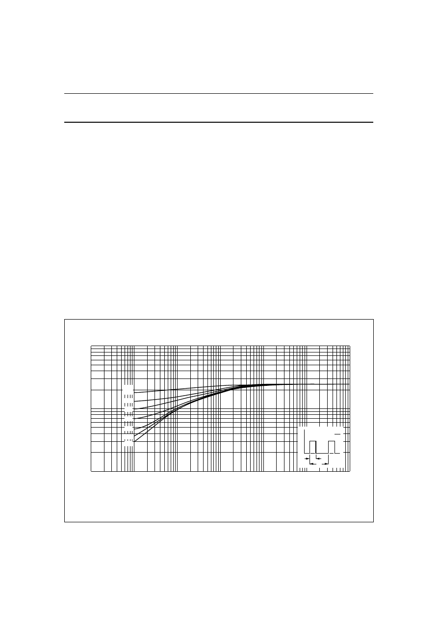
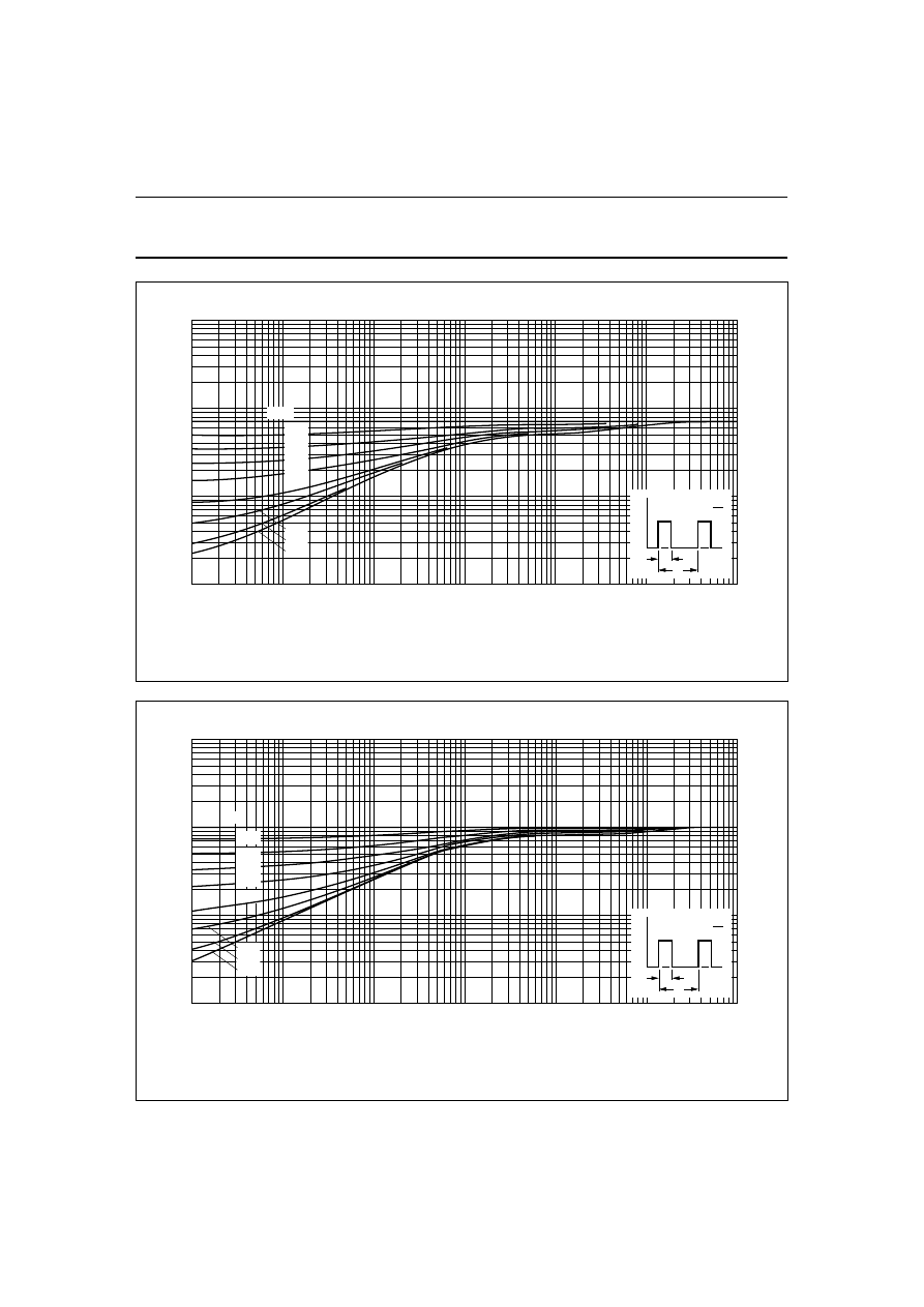
Reducing calculation time
To be able to point out the junction peak temperature at a
certain pulse time and duty cycle, a graph similar to that
shown in Fig.13 is included in relevant data sheets. In this
example, the curves have been derived using the formula
T
j(peak)
= T
ref
+ P
d
×
[
δ ×
R
th(j-ref)
+ (1
− δ
)
×
Z
th(t+w)
+
Z
th(w)
−
Z
th(t)
], with typical values inserted.
The pulse width along the X-axis meets a particular duty
cycle curve, indicating the Z
th
value in K/W along the
Y-axis.
T
j(peak)
= P
d(peak)
×
Z
th(j-s)
+ P
d(av)
×
R
th(s-a)
+ T
a
(
°
C)
Soldering point temperature provides a better reference
point than ambient temperature as this is subject to many
uncontrolled variables. Therefore, the thermal resistance
from junction to soldering point [R
th(j-s)
] is becoming a more
relevant measurement path.
Fig.13 Direct reading of thermal impedance from junction to soldering point for calculation of
junction temperature at pulsed power conditions.
handbook, full pagewidth
10
−
5
10
−
6
10
−
4
10
−
3
10
−
2
10
−
1
1
MBG388
10
3
10
2
10
Zth j-a
(K/W)
t p
T
P
t
t p
T
δ
=
tp (s)
δ
=
0.75
0.5
0.3
0.2
0.1
0.05
0
For transistors in small SMD packages which are usually
mounted on FR4 epoxy fibre-glass printed circuit boards,
only the thermal resistance from junction to ambient
[R
th(j-a)
] is published. In this case, the junction temperature
can be calculated by:
T
j(peak)
= P
d(peak)
×
Z
th(j-a)
+ T
a
(
°
C)
1997 Aug 20
15
Philips Semiconductors
Small-signal Transistors
General
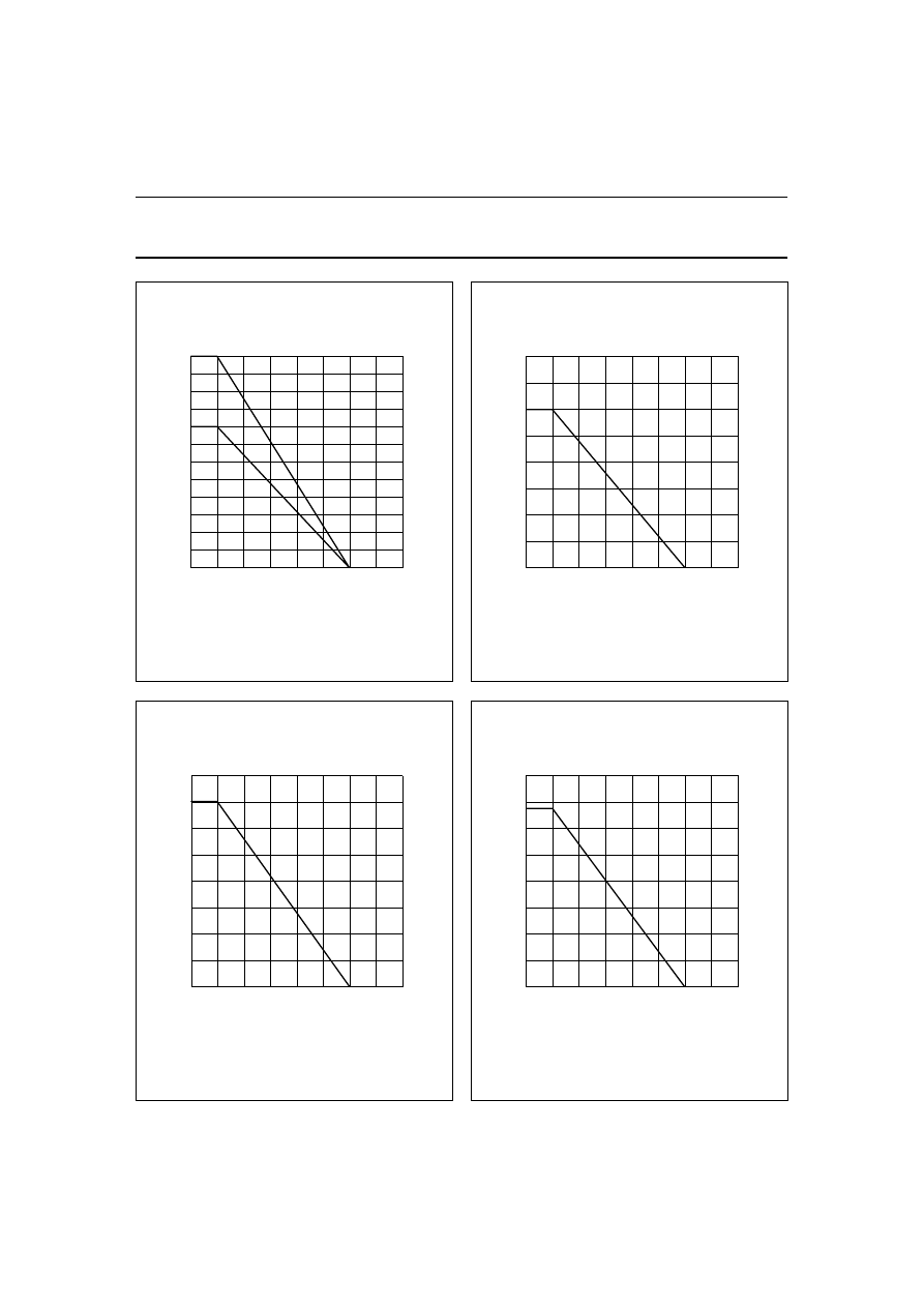
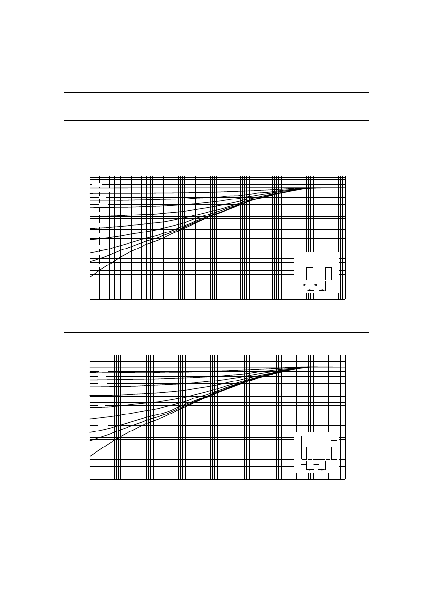
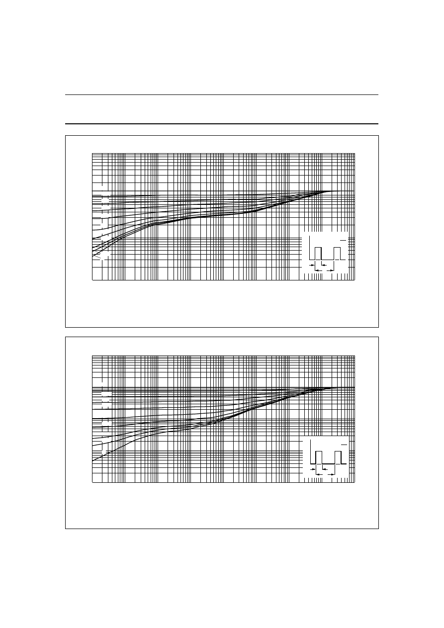
POWER DERATING CURVES FOR SMDs
Figures 14 through 32 on the following pages show the
power derating curves (P
tot
versus T
amb
) for transistors in
SMD packages.
Fig.14 Power derating curve for SOT23.
handbook, halfpage
0
200
300
0
100
200
100
MDA101
Ptot
(mW)
Tamb (
°
C)
Fig.15 Power derating curve for SOT143.
handbook, halfpage
0
200
300
0
100
200
100
MDA102
Ptot
(mW)
Tamb (
°
C)
Fig.16 Power derating curve for SC-59 (SOT346).
handbook, halfpage
0
200
300
0
100
200
100
MDA100
Ptot
(mW)
Tamb (
°
C)
Fig.17 Power derating curve for SC-70 (SOT323).
handbook, halfpage
0
200
300
0
100
200
100
MDA104
Ptot
(mW)
Tamb (
°
C)
1997 Aug 20
16
Philips Semiconductors
Small-signal Transistors
General
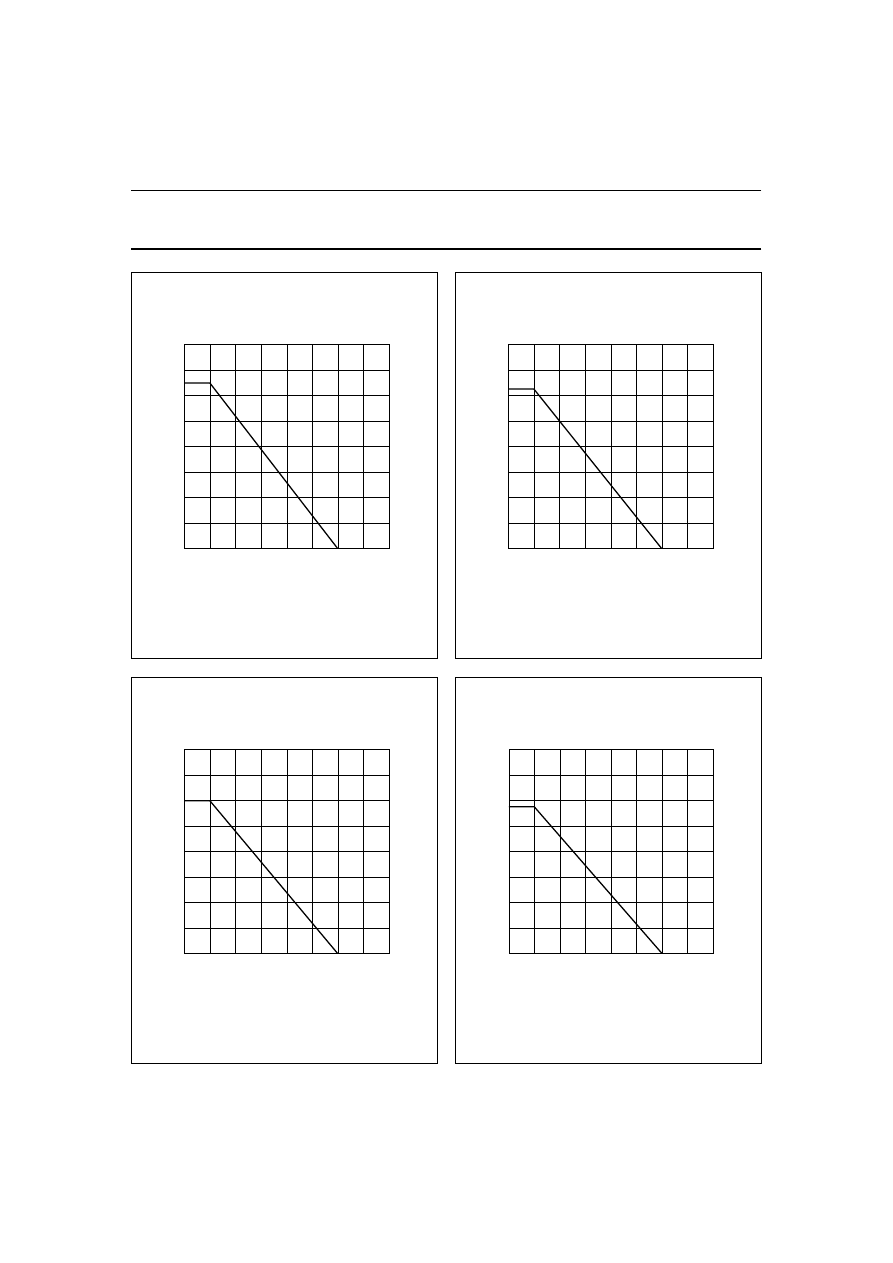
Fig.18 Power derating curves for SC-88 (SOT363).
handbook, halfpage
0
(1)
(2)
200
300
0
100
200
100
MDA103
Ptot
(mW)
Tamb (
°
C)
(1) All transistors used.
(2) One transistor used.
Fig.19 Power derating curve for SC-75 (SOT416).
handbook, halfpage
0
200
200
0
100
100
MDA105
Ptot
(mW)
Tamb (
°
C)
Fig.20 Power derating curve for SOT89.
Device families:
BC868, BC869, BSR30, BSR40.
handbook, halfpage
0
200
1.6
0
0.8
0.4
1.2
100
MDA113
Ptot
(W)
Tamb (
°
C)
Fig.21 Power derating curve for SOT89.
Device families:
BCX51, BCX54, BST15, BST50, BST60.
handbook, halfpage
0
200
1.6
0
0.8
0.4
1.2
100
MDA114
Ptot
(W)
Tamb (
°
C)
1997 Aug 20
17
Philips Semiconductors
Small-signal Transistors
General
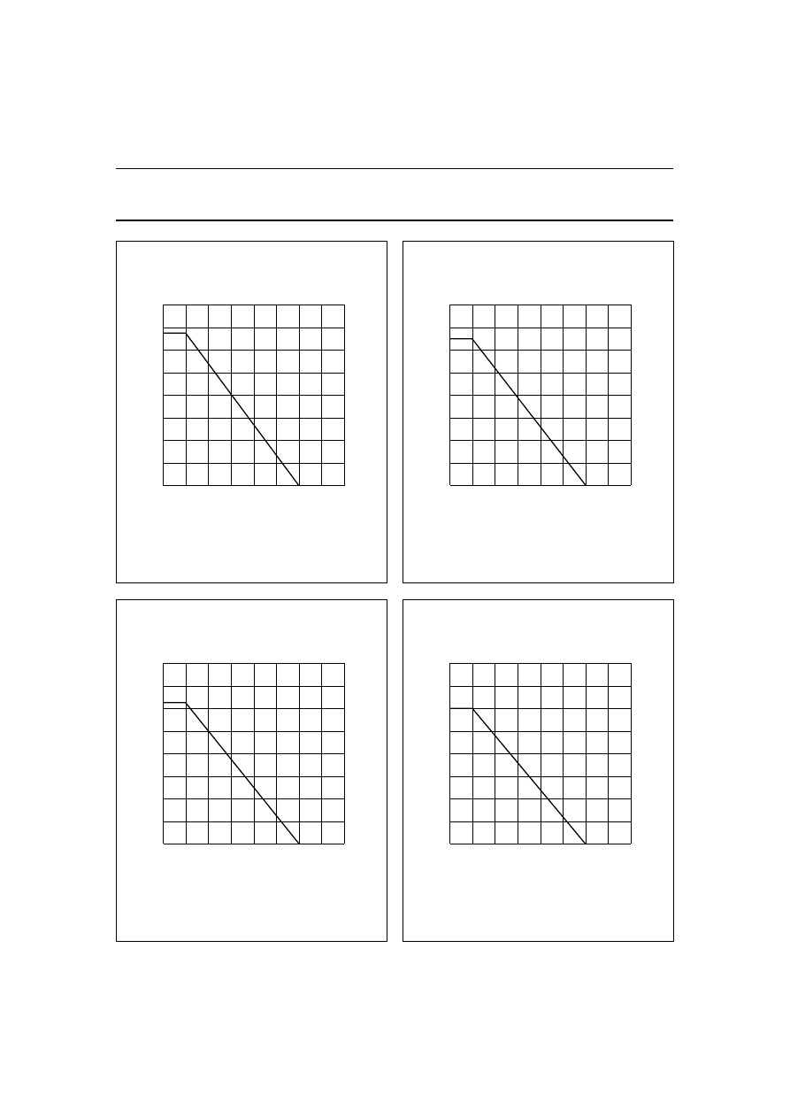
Fig.22 Power derating curve for SOT89.
Device families:
BCV28/48, BCV29/49, PXTA14, PXTA27, PXTA64.
handbook, halfpage
0
200
1.6
0
0.8
0.4
1.2
100
MDA115
Ptot
(W)
Tamb (
°
C)
Fig.23 Power derating curve for SOT89.
Device families:
BST39, PXTA42, PXTA92, PXT2907, PXT4403.
handbook, halfpage
0
200
1.6
0
0.8
0.4
1.2
100
MDA116
Ptot
(W)
Tamb (
°
C)
Fig.24 Power derating curve for SOT89.
Device families:
BF620, BF621, PXT2222A, PXT4401.
handbook, halfpage
0
200
1.6
0
0.8
0.4
1.2
100
MDA117
Ptot
(W)
Tamb (
°
C)
Fig.25 Power derating curve for SOT89.
Device families:
PXT3904, PXT3906.
handbook, halfpage
0
200
1.6
0
0.8
0.4
1.2
100
MDA118
Ptot
(W)
Tamb (
°
C)
1997 Aug 20
18
Philips Semiconductors
Small-signal Transistors
General
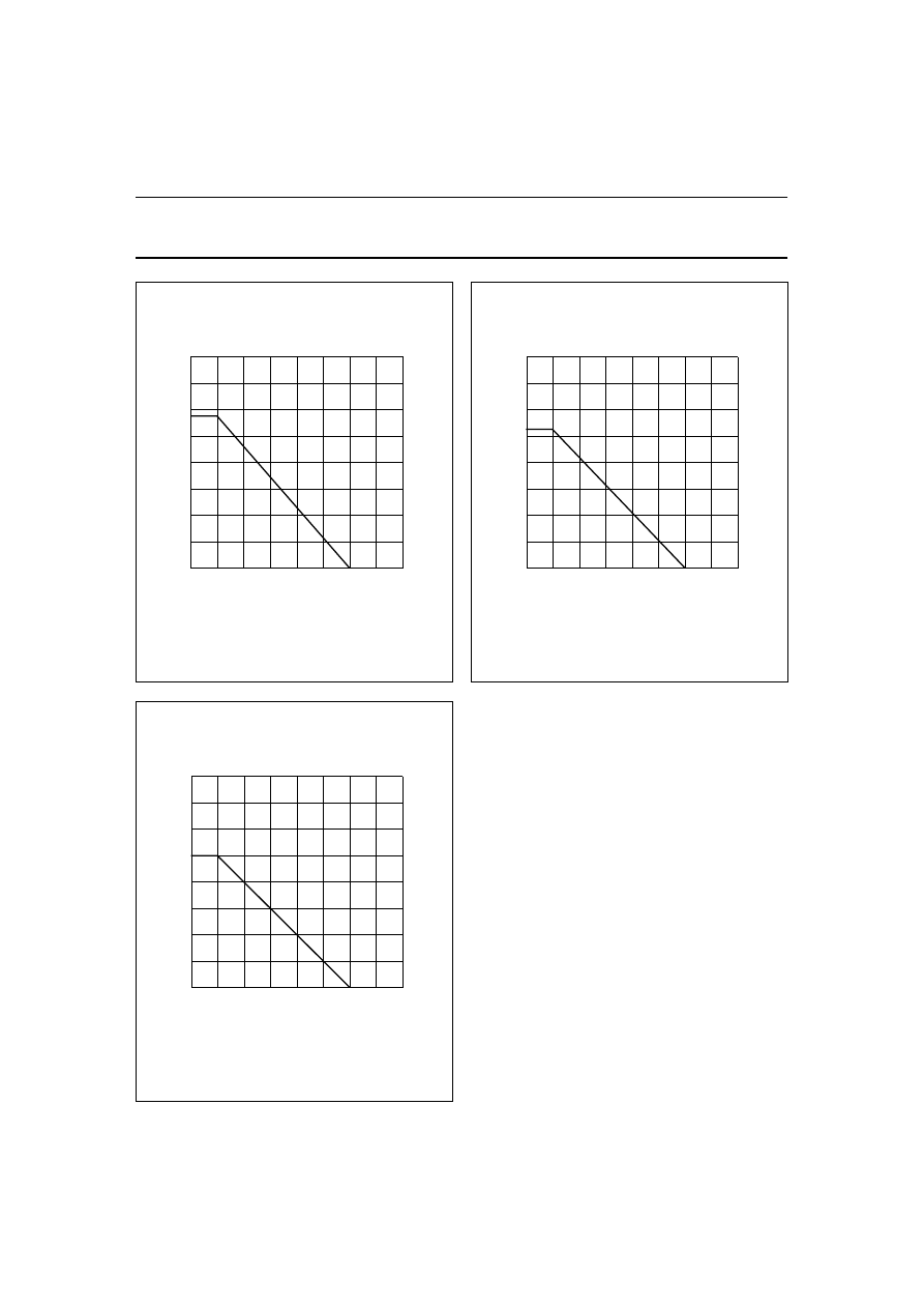
Fig.26 Power derating curve for SOT223.
Device families:
BCP68, BCP69, BDL31, BDL32, BDP31, BDP32, PZTA44.
handbook, halfpage
0
200
1.6
0
0.8
0.4
1.2
100
MDA106
Ptot
(W)
Tamb (
°
C)
Fig.27 Power derating curve for SOT223.
Device families:
BSP30, BSP40, BCP51, BCP54, BSP15.
handbook, halfpage
0
200
1.6
0
0.8
0.4
1.2
100
MDA107
Ptot
(W)
Tamb (
°
C)
Fig.28 Power derating curve for SOT223.
Device families:
BSP50, BSP60, BCP48, BCP49, PZTA13, PZTA63.
handbook, halfpage
0
200
1.6
0
0.8
0.4
1.2
100
MDA108
Ptot
(W)
Tamb (
°
C)
Fig.29 Power derating curve for SOT223.
Device families:
PZTA05, PZTA55, BF720, BF721, BSP19, PZTA42, PZTA92.
handbook, halfpage
0
200
1.6
0
0.8
0.4
1.2
100
MDA109
Ptot
(W)
Tamb (
°
C)
1997 Aug 20
19
Philips Semiconductors
Small-signal Transistors
General
Fig.30 Power derating curve for SOT223.
Device families:
PZTA2907A, PZT4403, PZT2222A, PZT4401, PZT5401, PZT5551.
handbook, halfpage
0
200
1.6
0
0.8
0.4
1.2
100
MDA110
Ptot
(W)
Tamb (
°
C)
Fig.31 Power derating curve for SOT223.
Device families:
PZT3904, PZT3906.
handbook, halfpage
0
200
1.6
0
0.8
0.4
1.2
100
MDA111
Ptot
(W)
Tamb (
°
C)
Fig.32 Power derating curve for SOT223.
Device family:
PZT2369A.
handbook, halfpage
0
200
1.6
0
0.8
0.4
1.2
100
MDA112
Ptot
(W)
Tamb (
°
C)
1997 Aug 20
20
Philips Semiconductors
Small-signal Transistors
General
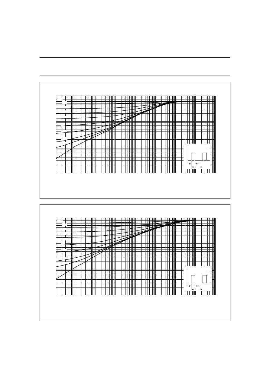
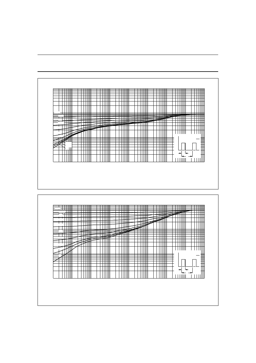
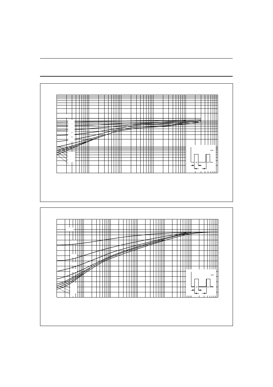
THERMAL IMPEDANCE CURVES
Figures 33 through 54 on the following pages show the thermal impedance curves (Z
th
versus t
p
) for various duty cycles.
Fig.33 Thermal impedance curves (junction to ambient) for transistors mounted onto a PCB for SOT23.
handbook, full pagewidth
10
3
10
2
Zth j-a
(K/W)
10
1
MGL193
10
−
5
10
−
4
10
−
3
10
−
2
10
−
1
1
tp (s)
10
10
2
10
3
tp
tp
T
P
t
T
δ
=
δ
= 1
0.75
0.5
0.33
0.2
0.1
0.05
0
0.01
0.02
Fig.34 Thermal impedance curves (junction to ambient) for transistors mounted onto a PCB for SOT143.
handbook, full pagewidth
10
3
10
2
10
Zth j-a
(K/W)
1
MGL194
10
−
5
10
−
4
10
−
3
10
−
2
10
−
1
1
tp (s)
10
10
2
10
3
tp
tp
T
P
t
T
δ
=
δ
= 1
0.75
0.5
0.33
0.2
0.1
0.05
0
0.01
0.02

1997 Aug 20
21
Philips Semiconductors
Small-signal Transistors
General
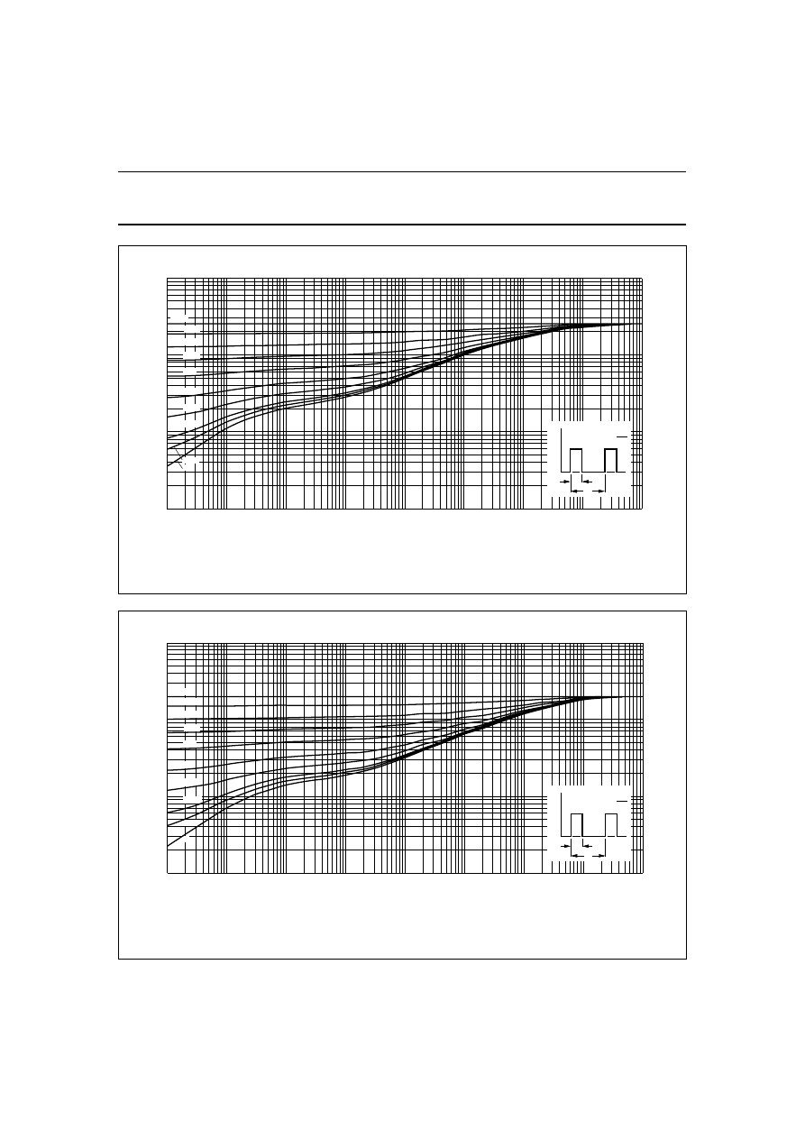
Fig.35 Thermal impedance curves (junction to ambient) for transistors mounted onto a PCB for SC-59 (SOT346).
handbook, full pagewidth
10
3
10
2
10
Zth j-a
(K/W)
1
MGL195
10
−
5
10
−
4
10
−
3
10
−
2
10
−
1
1
tp (s)
10
10
2
10
3
tp
tp
T
P
t
T
δ
=
δ
= 1
0.75
0.5
0.33
0.2
0.1
0.05
0
0.01
0.02
Fig.36 Thermal impedance curves (junction to ambient) for transistors mounted onto a PCB for SC-70 (SOT323).
handbook, full pagewidth
10
3
10
2
10
Zth j-a
(K/W)
1
MGL196
10
−
5
10
−
4
10
−
3
10
−
2
10
−
1
1
tp (s)
10
10
2
10
3
tp
tp
T
P
t
T
δ
=
δ
= 1
0.75
0.5
0.33
0.2
0.1
0.05
0
0.01
0.02
1997 Aug 20
22
Philips Semiconductors
Small-signal Transistors
General
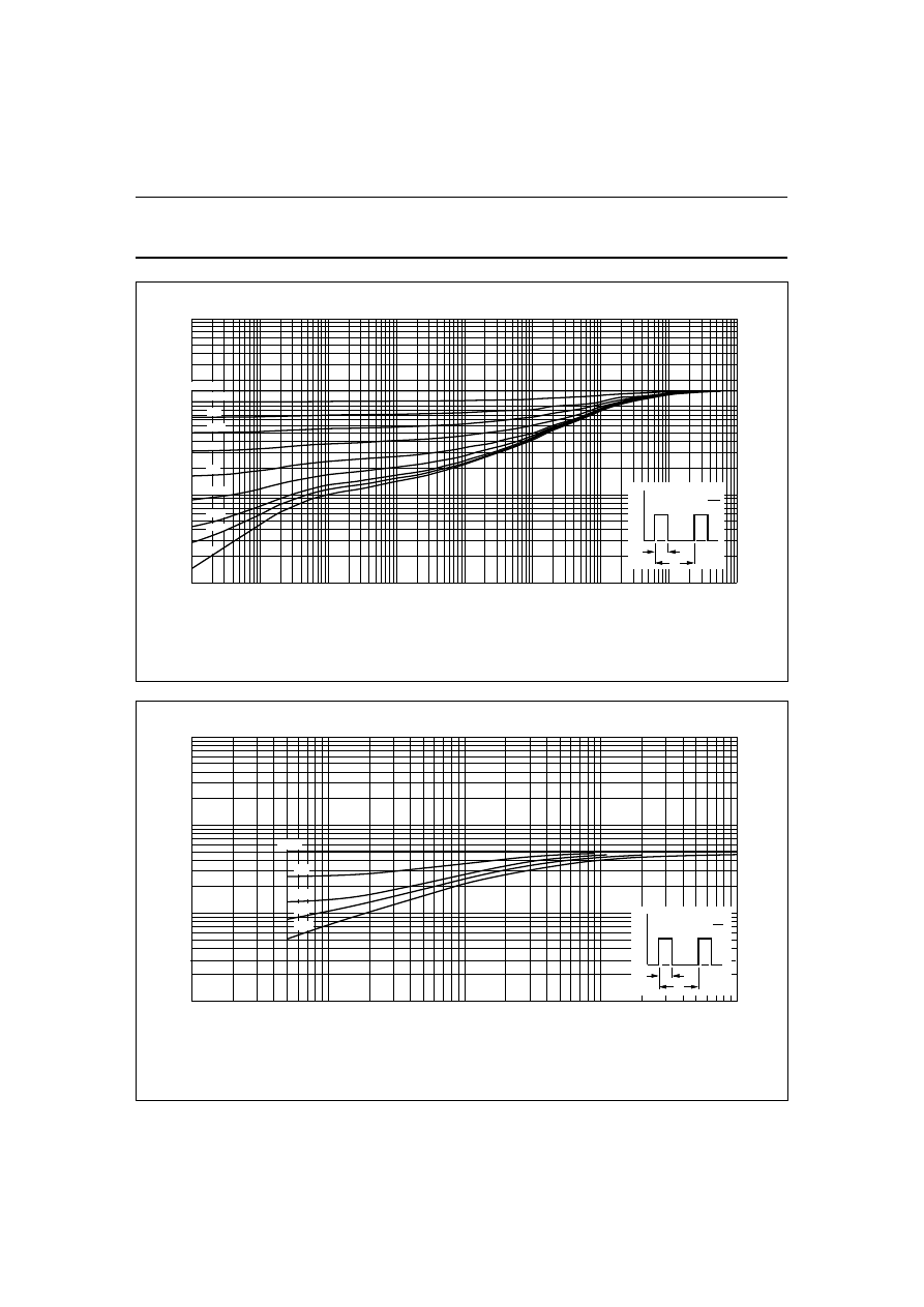
Fig.37 Thermal impedance curves (junction to ambient) for transistors mounted onto a PCB for SC-88 (SOT363).
handbook, full pagewidth
10
3
10
2
10
Zth j-a
(K/W)
1
MGL197
10
−
5
10
−
4
10
−
3
10
−
2
10
−
1
1
tp (s)
10
10
2
10
3
tp
tp
T
P
t
T
δ
=
δ
= 1
0.75
0.5
0.33
0.2
0.1
0.05
0
0.01
0.02
Fig.38 Thermal impedance curves (junction to ambient) for transistors mounted onto a PCB for SC-75 (SOT416).
handbook, full pagewidth
10
3
10
2
10
Zth j-a
(K/W)
1
MGL198
10
−
5
10
−
4
10
−
3
10
−
2
10
−
1
1
tp (s)
10
10
2
10
3
tp
tp
T
P
t
T
δ
=
δ
= 1
0.75
0.5
0.33
0.2
0.1
0.05
0
0.01
0.02
1997 Aug 20
23
Philips Semiconductors
Small-signal Transistors
General
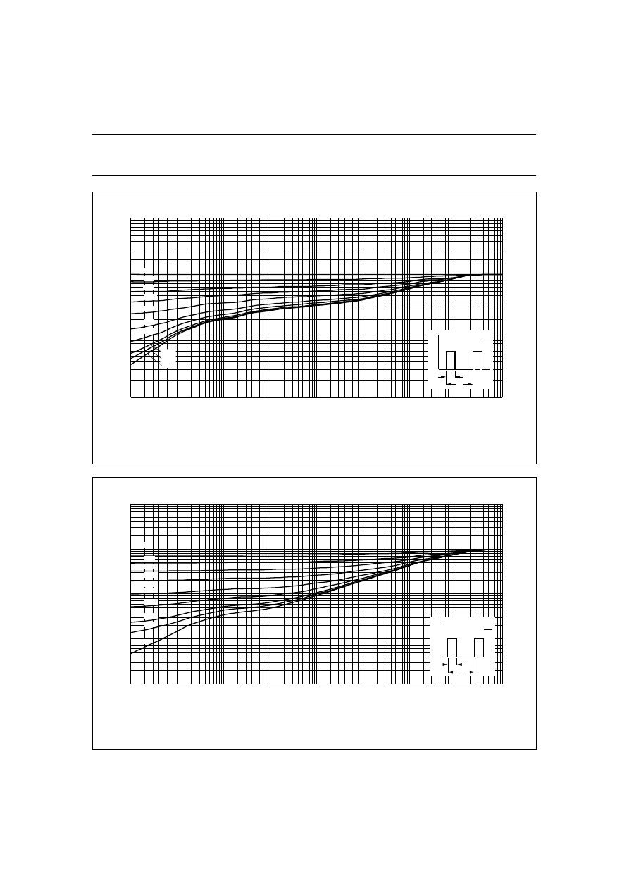
Fig.39 Thermal impedance curves (junction to ambient) for transistors mounted onto a PCB for SOT89.
handbook, full pagewidth
10
3
10
2
Zth j-a
(K/W)
10
1
MGD875
10
−
5
10
−
4
10
−
3
10
−
2
10
−
1
1
tp (s)
10
10
2
10
3
tp
tp
T
P
t
T
δ
=
δ
= 1
0.7
0.5
0.33
0.2
0.1
0.05
0.02
0.01
0
PCB, single-sided, unplated, Rth j-s = 25 K/W, Rth j-a = 113 K/W.
See also Fig.10 curve (1).
Fig.40 Thermal impedance curves (junction to ambient) for transistors mounted onto a PCB for SOT89.
handbook, full pagewidth
10
3
10
2
10
Zth j-a
(K/W)
1
10
−
1
MGD874
10
−
5
10
−
4
10
−
3
10
−
2
10
−
1
1
tp (s)
10
10
2
10
3
δ
= 1
0.7
0.5
0.33
0.2
0.1
0
0.01
0.05
0.02
tp
tp
T
P
t
T
δ
=
PCB, single-sided, plated, Rth j-s = 7 K/W, Rth j-a = 95 K/W.
See also Fig.10 curve (2).
1997 Aug 20
24
Philips Semiconductors
Small-signal Transistors
General
Fig.41 Thermal impedance curves (junction to ambient) for transistors mounted onto a PCB for SOT89.
handbook, full pagewidth
10
2
1
10
MGD873
10
−
5
10
−
4
10
−
3
10
−
2
10
−
1
1
Zth j-a
(K/W)
tp (s)
10
10
2
10
3
δ
= 1
0.7
0.5
0.33
0.2
0.1
0.05
0.02
0.01
0
tp
tp
T
P
t
T
δ
=
PCB, double-sided, unplated, Rth j-s = 25 K/W, Rth j-a = 76 K/W.
See also Fig.10 curve (3).
Fig.42 Thermal impedance curves (junction to ambient) for transistors mounted onto a PCB for SOT89.
handbook, full pagewidth
10
2
10
Zth j-a
(K/W)
1
10
−
1
MGD872
10
−
5
10
−
4
10
−
3
10
−
2
10
−
1
1
tp (s)
10
10
2
10
3
tp
tp
T
P
t
T
δ
=
δ
= 1
0.75
0.5
0.33
0.2
0.1
0.05
0
0.01
0.02
PCB, double-sided, plated, Rth j-s = 7 K/W, Rth j-a = 58 K/W.
See also Fig.10 curve (4).
1997 Aug 20
25
Philips Semiconductors
Small-signal Transistors
General
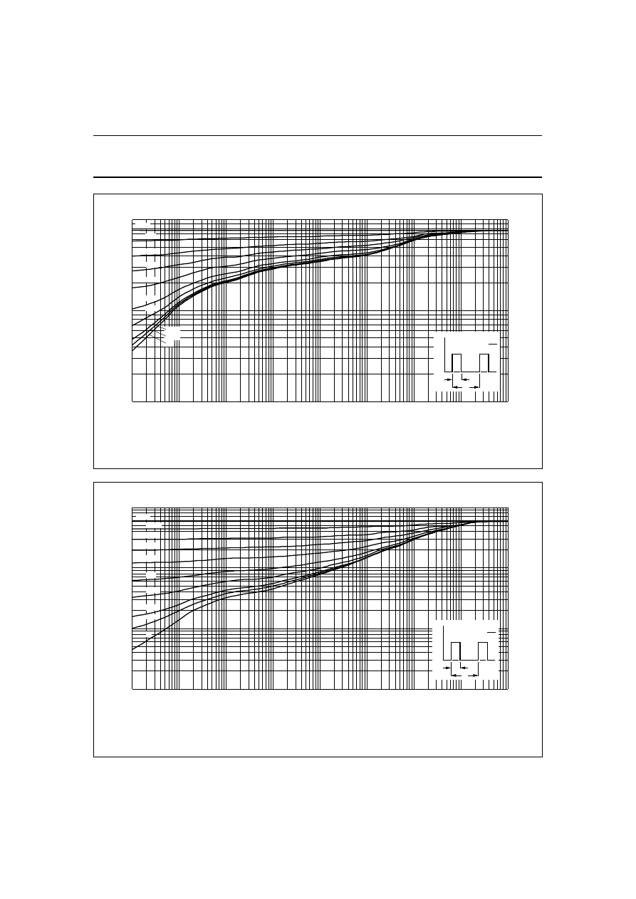
Fig.43 Thermal impedance curves (junction to ambient) for transistors mounted onto a PCB for SOT223.
PCB, single-sided, unplated, Rth j-s = 36 K/W, Rth j-a = 124 K/W.
See also Fig.10 curve (1).
handbook, full pagewidth
10
3
10
2
10
Zth j-a
(K/W)
1
MGL202
10
−
5
10
−
4
10
−
3
10
−
2
10
−
1
1
tp (s)
10
10
2
10
3
tp
tp
T
P
t
T
δ
=
δ
= 1
0.75
0.5
0.33
0.2
0.1
0.05
0
0.01
0.02
Fig.44 Thermal impedance curves (junction to ambient) for transistors mounted onto a PCB for SOT223.
handbook, full pagewidth
10
3
10
2
10
Zth j-a
(K/W)
1
10
−
1
MGD869
10
−
5
10
−
4
10
−
3
10
−
2
10
−
1
1
tp (s)
10
10
2
10
3
δ
= 1
0.75
0.5
0.33
0.2
0.1
0
0.01
0.05
0.02
tp
tp
T
P
t
T
δ
=
PCB, single-sided, plated, Rth j-s = 10 K/W, Rth j-a = 98 K/W.
See also Fig.10 curve (2).
1997 Aug 20
26
Philips Semiconductors
Small-signal Transistors
General
Fig.45 Thermal impedance curves (junction to ambient) for transistors mounted onto a PCB for SOT223.
handbook, full pagewidth
10
3
10
2
Zth j-a
(K/W)
10
1
MGD868
10
−
5
10
−
4
10
−
3
10
−
2
10
−
1
1
tp (s)
10
10
2
10
3
tp
tp
T
P
t
T
δ
=
δ
= 1
0.75
0.5
0.33
0.2
0.1
0.05
0.02
0.01
0
PCB, double-sided, unplated, Rth j-s = 36 K/W, Rth j-a = 87 K/W.
See also Fig.10 curve (3).
Fig.46 Thermal impedance curves (junction to ambient) for transistors mounted onto a PCB for SOT223.
handbook, full pagewidth
10
2
10
Zth j-a
(K/W)
1
10
−
1
MGD867
10
−
5
10
−
4
10
−
3
10
−
2
10
−
1
1
tp (s)
10
10
2
10
3
tp
tp
T
P
t
T
δ
=
δ
= 1
0.75
0.5
0.33
0.2
0.1
0.05
0
0.01
0.02
PCB, double-sided, plated, Rth j-s = 10 K/W, Rth j-a = 61 K/W.
See also Fig.10 curve (4).
1997 Aug 20
27
Philips Semiconductors
Small-signal Transistors
General
Fig.47 Thermal impedance curves (junction to ambient) for transistors mounted onto a PCB for SOT54.
Curves are for devices with P
tot
= 500 mW.
handbook, full pagewidth
10
3
10
2
10
Zth j-a
(K/W)
1
MGL199
10
−
5
10
−
4
10
−
3
10
−
2
10
−
1
1
tp (s)
10
10
2
10
3
tp
tp
T
P
t
T
δ
=
δ
= 1
0.75
0.5
0.33
0.2
0.1
0.05
0
0.01
0.02
Fig.48 Thermal impedance curves (junction to ambient) for transistors mounted onto a PCB for SOT54.
Curves are for devices with P
tot
= 625 mW.
handbook, full pagewidth
10
3
10
2
10
Zth j-a
(K/W)
1
MGL200
10
−
5
10
−
4
10
−
3
10
−
2
10
−
1
1
tp (s)
10
10
2
10
3
tp
tp
T
P
t
T
δ
=
δ
= 1
0.75
0.5
0.33
0.2
0.1
0.05
0
0.01
0.02
1997 Aug 20
28
Philips Semiconductors
Small-signal Transistors
General
Fig.49 Thermal impedance curves (junction to ambient) for transistors mounted onto a PCB for SOT54.
Curves are for devices with P
tot
= 830 mW.
handbook, full pagewidth
10
3
10
2
10
Zth j-a
(K/W)
1
MGL201
10
−
5
10
−
4
10
−
3
10
−
2
10
−
1
1
tp (s)
10
10
2
10
3
tp
tp
T
P
t
T
δ
=
δ
= 1
0.75
0.5
0.33
0.2
0.1
0.05
0
0.01
0.02
Fig.50 Thermal impedance curves (junction to mounting-base) for transistors mounted onto a PCB
for TO-126 (SOT32).
handbook, full pagewidth
10
2
10
−
1
10
−
2
10
−
1
1
10
10
2
tp (ms)
10
1
Zth j-mb
(K/W)
MGG837
tp
tp
T
P
t
T
δ
=
δ
= 1
0.5
0.2
0.1
0.01
Device example: BDX35.
1997 Aug 20
29
Philips Semiconductors
Small-signal Transistors
General
Fig.51 Thermal impedance curves (junction to mounting-base) for transistors mounted onto a PCB
for TO-126 (SOT32).
handbook, full pagewidth
10
10
−
1
10
2
10
−
3
10
−
2
10
−
1
1
10
tp (ms)
10
2
10
3
1
Zth j-mb
(K/W)
MGG835
tp
tp
T
P
t
T
δ
=
δ
= 1
0.75
0.50
0.33
0.20
0.05
0.02
0.01
0.10
Device example: BD226.
Fig.52 Thermal impedance curves (junction to mounting-base) for transistors mounted onto a PCB
for TO-126 (SOT32).
handbook, full pagewidth
10
2
10
−
1
10
−
6
10
−
5
10
−
4
10
−
3
10
−
2
10
−
1
tp (s)
1
10
1
Zth j-mb
(K/W)
MGG832
tp
tp
T
P
t
T
δ
=
δ
= 1
0.75
0.50
0.33
0.10
0.20
0.05
0.02
0.01
Device example: BD136.
1997 Aug 20
30
Philips Semiconductors
Small-signal Transistors
General
Fig.53 Thermal impedance curves (junction to mounting-base) for transistors mounted onto a PCB
for TO-202 (SOT128).
handbook, full pagewidth
10
10
−
1
10
2
10
−
2
10
−
1
1
10
tp (ms)
10
2
10
3
1
Zth j-mb
(K/W)
MGG836
tp
tp
T
P
t
T
δ
=
δ
= 1
0.75
0.50
0.33
0.10
0.20
0.05
0.02
0.01
0
Device example: BD839.
Fig.54 Thermal impedance curves (junction to mounting-base) for transistors mounted onto a PCB
for TO-202 (SOT128).
handbook, full pagewidth
30
0
10
20
MGG833
1
10
10
2
10
3
10
4
10
−
2
10
−
1
tp (ms)
Zth j-mb
(K/W)
tp
tp
T
P
t
T
δ
=
δ
= 1
0.10
0.05
0.02
0
0.75
0.50
0.33
0.20
Device example: BF869.
Wyszukiwarka
Podobne podstrony:
SC04 CONVERSION 1996 1
SC04 MARKING 1996 1
1996 05 Generator m cz − próbnik
FALOMIERZ GENERATOR EDW 7 1996
Eurocode 6 Part 1 2 1996 2005 Design of Masonry Structures General Rules Structural Fire Design
1996 01 Najprostszy generator melodii
Bayesian Methods A General Introduction [jnl article] E Jaynes (1996) WW
1996 07 Falomierz − generator w cz (TDO)
SC17 GENERAL APP 1996 1
SC17 GENERAL TEMP 1996 3
1996 05 Generator m cz − próbnik
SC17 GENERAL ANG 1996 3
1996 GeneralTassoFragoso
FALOMIERZ GENERATOR EDW 7 1996
Eurocode 6 Part 1 1 1996 2005 Design of Masonry Structures General Rules for Reinforced and Unre
15 Sieć Następnej Generacjiid 16074 ppt
Solid Edge Generator kół zębatych
więcej podobnych podstron