
HA13151, HA13152
14 W
×
4-Channel BTL Power IC
ADE-207-116
1st. Edition
Description
The HA13151/HA13152 are high output and low distortion 4 ch BTL power IC designed for digital car
audio.
At 13.2 V to 4
Ω
load, this power IC provides output power 14 W with 10% distortion.
Functions
•
4 ch BTL power amplifiers
•
Built-in standby circuit
•
Built-in muting circuit
•
Built-in protection circuit (surge, T.S.D, and ASO)
Features
•
Few external parts lead to compact set-area possibility
•
Popping noise minimized
•
Low output noise
•
Built-in high reliability protection circuit
HA13151, HA13152
2
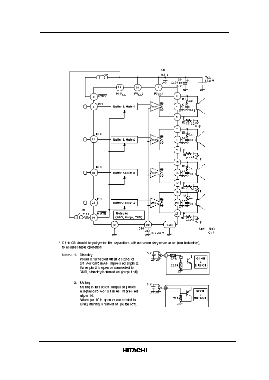
Block Diagram
Absolute Maximum Ratings (Ta = 25°C)
Item
Symbol
Rating
Unit
Remarks
HA13151, HA13152
3
Operating supply voltage
V
CC
18
V
Supply voltage when no signal*
1
V
CC
(DC)
26
V
Peak supply voltage*
2
V
CC
(PEAK)
50
V
Output current*
3
I
O
(PEAK)
3
A
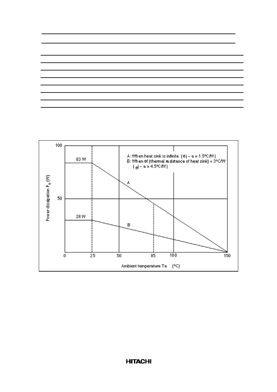
Power dissipation*
4
P
T
83
W
Junction temperature
Tj
150
°C
Operating temperature
Topr
–30 to +85
°C
Storage temperature
Tstg
–55 to +125
°C
Notes: 1. Tolerance within 30 seconds
2. Tolerance in surge pulse waveform
3. Value per 1 channel
4. Value when attached on the infinite heat sink plate at Ta = 25 °C.
The derating carve is as shown in the graph below.
HA13151, HA13152
4
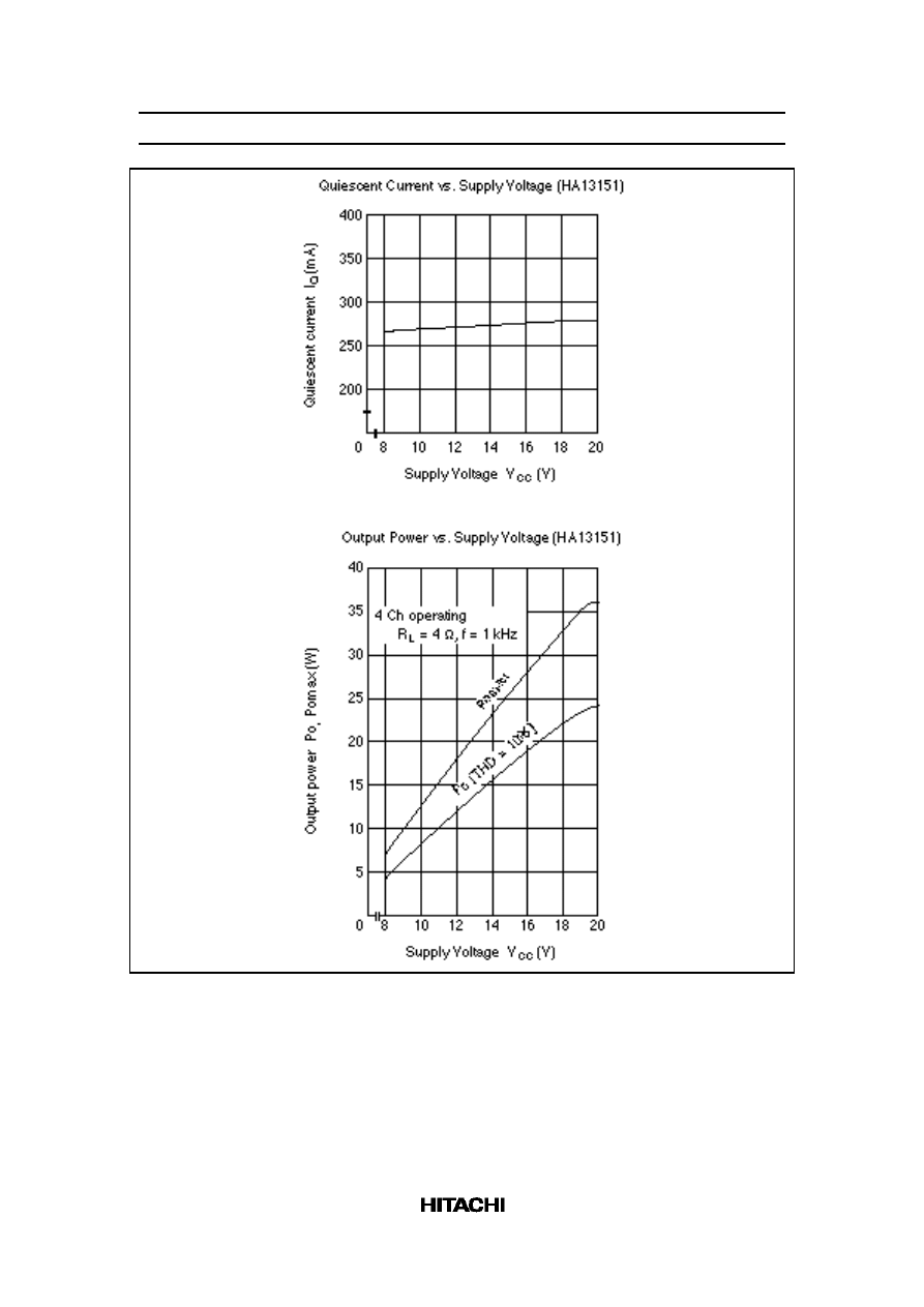
Electrical Characteristics (V
CC
= 13.2 V, f = 1 kHz, R
L
= 4
Ω
, Rg = 600
Ω
, Ta =
25°C)
HA13151
Item
Symbol
Min
Typ
Max
Unit
Test Conditions
Quiescent current
I
Q
1
—
270
—
mA
Vin = 0
Output offset voltage
∆
V
Q
–300
0
+300
mV
Gain
G
V
30.5
32
33.5
dB
Gain difference between
channels
∆
G
V
–1.5
0
+1.5
dB
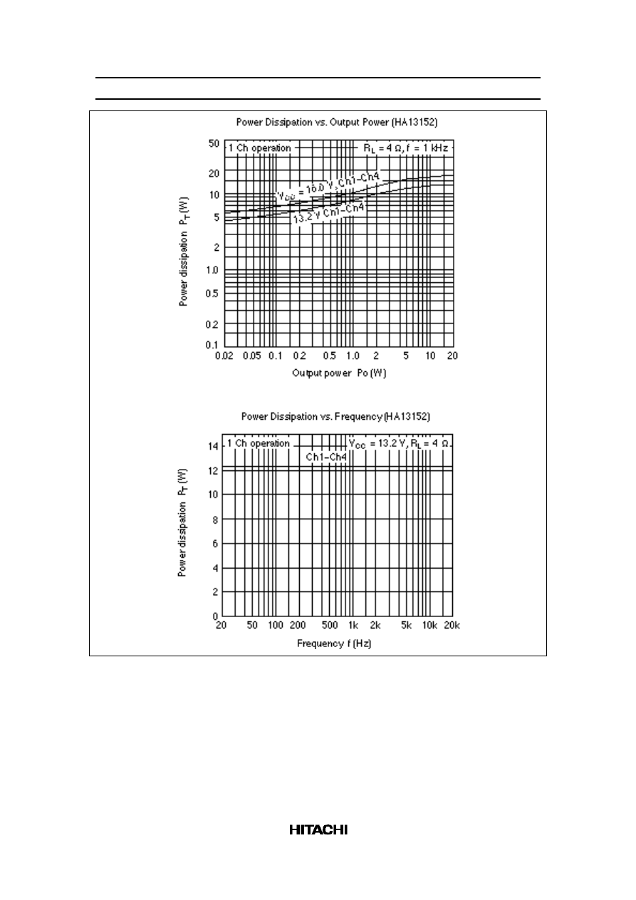
Rated output power
Po
—
14
—
W
V
CC
= 13.2 V
THD = 10%, R
L
= 4
Ω
Max output power
Pomax
—
22
—
W
V
CC
= 13.7 V
THD = Max, R
L
= 4
Ω
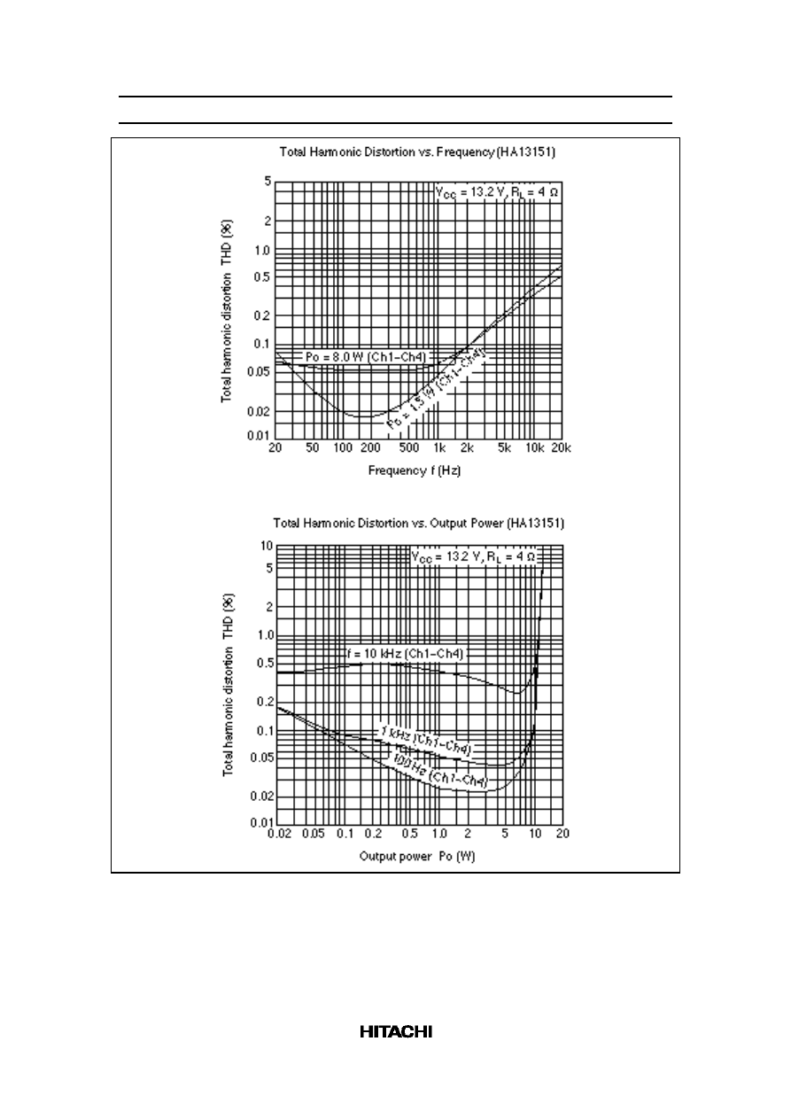
Total harmonic distortion
T.H.D.
—
0.05
—
%
Po = 3 W
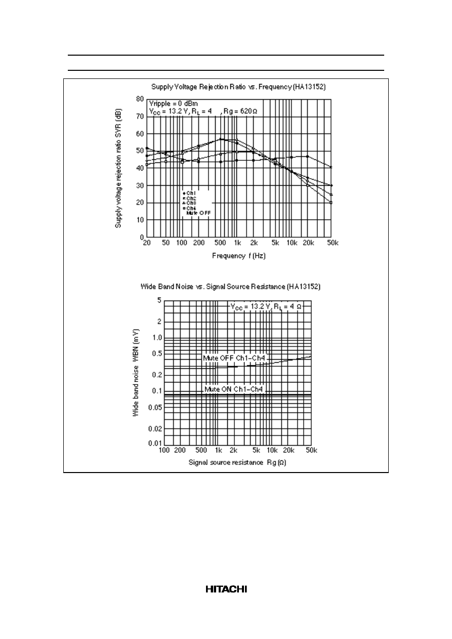
Output noise voltage
WBN
—
0.15
—
mVrms
Rg = 0
Ω
BW = 20 to 20 kHz
Ripple rejection
SVR
—
55
—
dB
Rg = 600
Ω
, f = 120 Hz
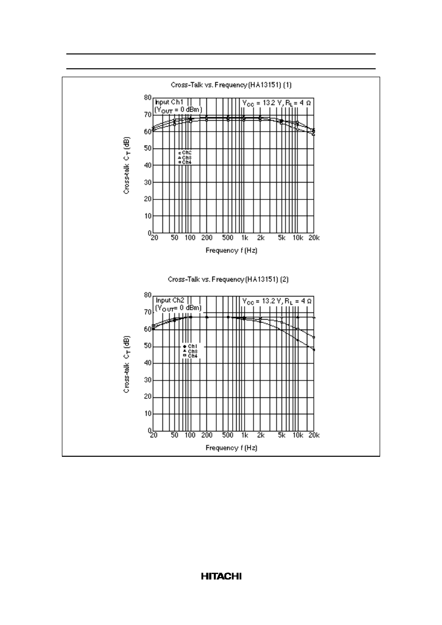
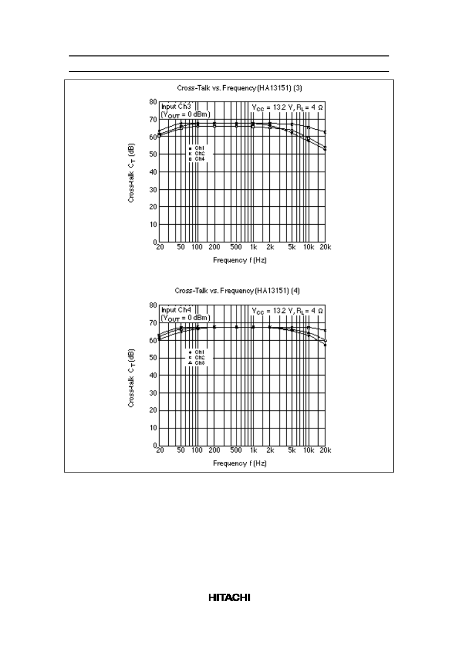
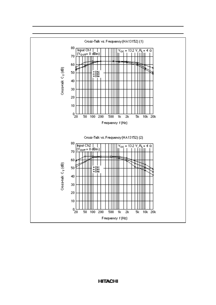
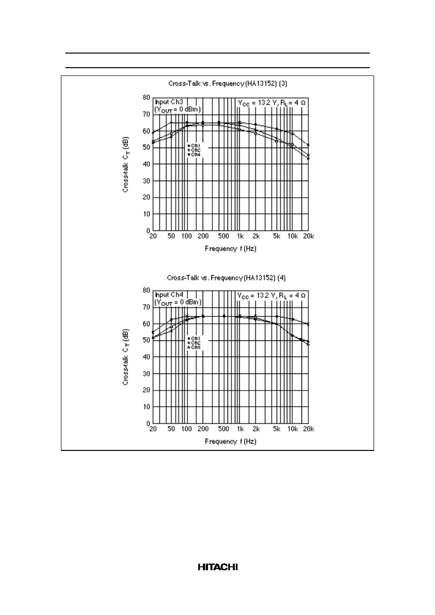
Channel cross talk
C.T.
—
70
—
dB
Rg = 600
Ω
Vout = 0 dBm
Input impedance
Rin
—
25
—
k
Ω
Standby current
I
Q
2
—
—
200
µA
Standby control voltage
(high)
V
STH
3.5
—
V
CC
V
Standby control voltage
(low)
V
STL
0
—
1.5
V
Muting control voltage
(high)
V
MH
3.5
—
V
CC
V
Muting control voltage
(low)
V
ML
0
—
1.5
V
Muting attenuation
ATTM
—
70
—
dB
Vout = 0 dBm
HA13151, HA13152
5
HA13152
Item
Symbol
Min
Typ
Max
Unit
Test Conditions
Quiescent current
I
Q
1
—
270
—
mA
Vin = 0
Output offset voltage
∆
V
Q
–300
0
+300
mV
Gain
G
V
38.5
40
41.5
dB
Gain difference between
channels
∆
G
V
–1.5
0
+1.5
dB
Rated output power
Po
—
14
—
W
V
CC
= 13.2 V
THD = 10%, R
L
= 4
Ω
Max output power
Pomax
—
22
—
W
V
CC
= 13.7 V
THD = Max, R
L
= 4
Ω
Total harmonic distortion
T.H.D.
—
0.05
—
%
Po = 3%
Output noise voltage
WBN
—
0.25
—
mVrms
Rg = 0
Ω
BW = 20 to 20 kHz
Ripple rejection
SVR
—
45
—
dB
Rg = 600
Ω
, f = 120 Hz
Channel cross talk
C.T.
—
60
—
dB
Rg = 600
Ω
Vout = 0 dBm
Input impedance
Rin
—
25
—
k
Ω
Standby current
I
Q
2
—
—
200
µA
Standby control voltage
(high)
V
STH
3.5
—
V
CC
V
Standby control voltage
(low)
V
STL
0
—
1.5
V
Muting control voltage
(high)
V
MH
3.5
—
V
CC
V
Muting control voltage
(low)
V
ML
0
—
1.5
V
Muting attenuation
ATTM
—
60
—
dB
Vout = 0 dBm
HA13151, HA13152
6
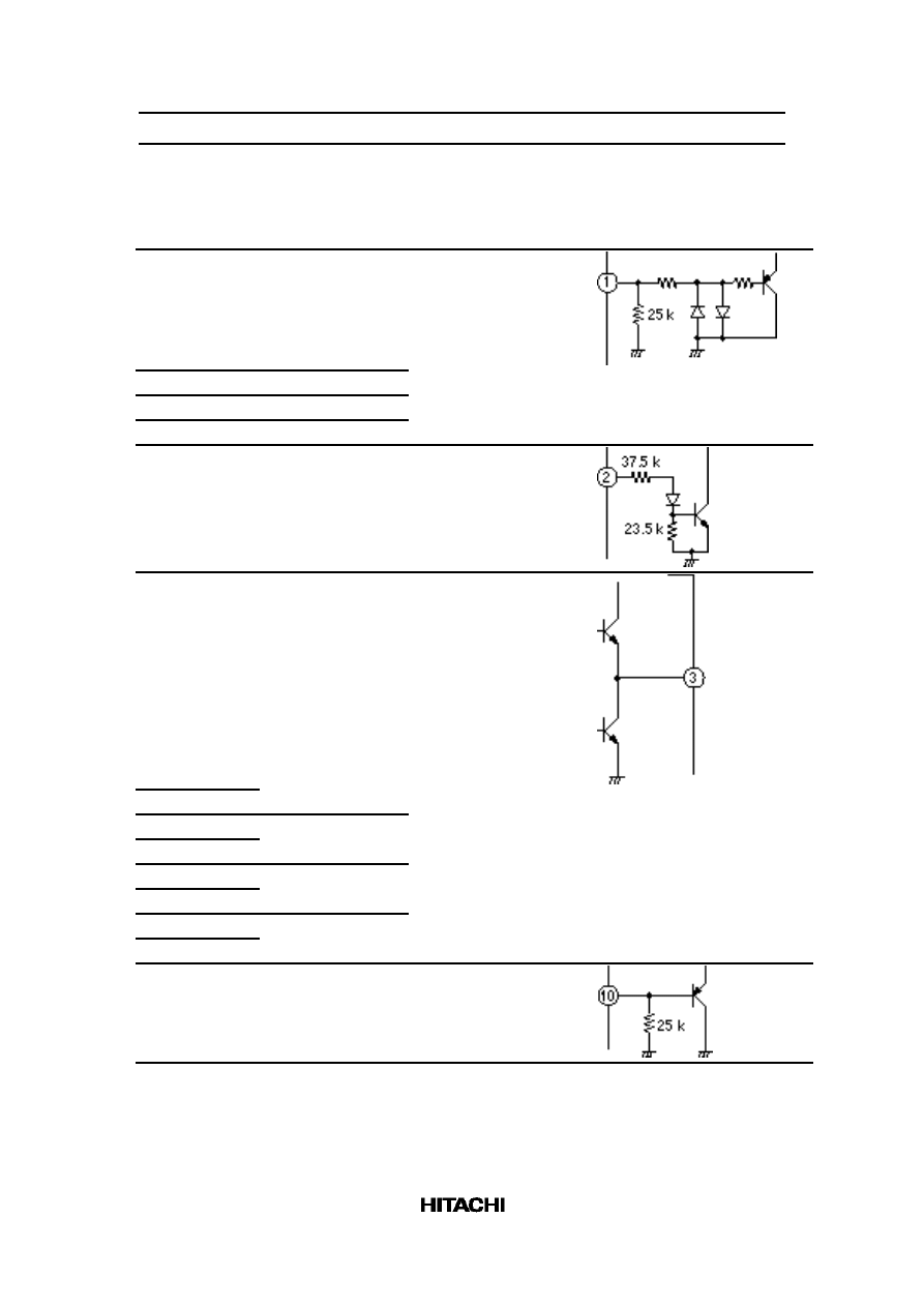
Pin Explanation
Pin
No.
Symbol
Functions
Input
Impedance
DC
Voltage
Equivalence Circuit
1
IN1
CH1 INPUT
25 k
Ω
(Typ)
0 V
11
IN2
CH2 INPUT
13
IN3
CH3 INPUT
23
IN4
CH4 INPUT
2
STBY
Standby control
90 k
Ω
(at Trs. cutoff)
—
3
OUT1 +
CH1 OUTPUT
—
V
CC
/2
5
OUT1 –
7
OUT2 +
CH2 OUTPUT
9
OUT2 –
15
OUT3 +
CH3 OUTPUT
17
OUT3 –
19
OUT4 +
CH4 OUTPUT
21
OUT4 –
10
MUTE
Muting control
25 k
Ω
(Typ)
—
HA13151, HA13152
7
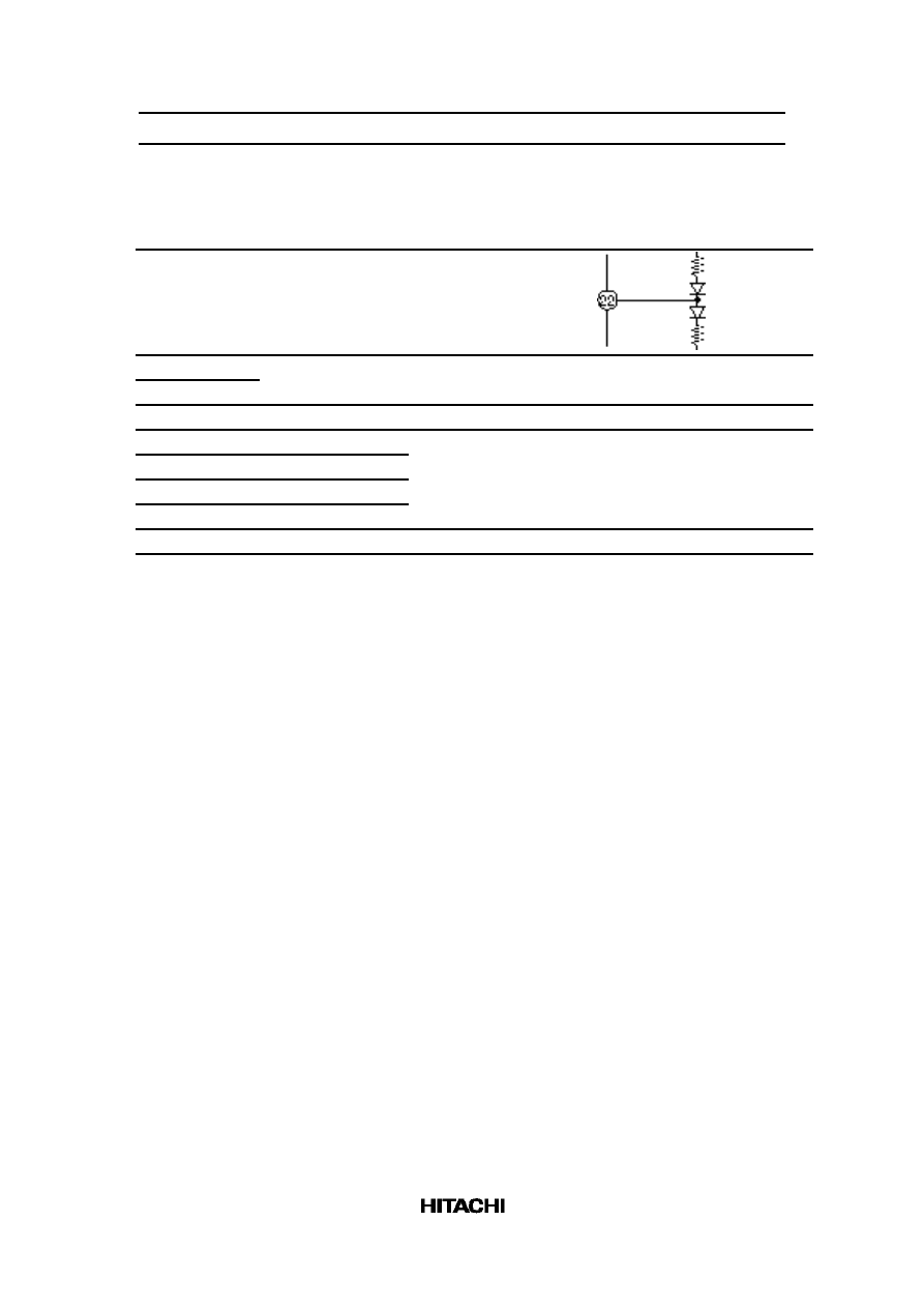
Pin Explanation (cont)
Pin
No.
Symbol
Functions
Input
Impedance
DC
Voltage
Equivalence Circuit
22
RIPPLE
Bias stability
—
V
CC
/2
6
PV
CC
1
Power of output stage
—
V
CC
—
18
PV
CC
2
14
INV
CC
Power of input stage
—
V
CC
—
4
CH1 GND
CH1 power GND
—
—
—
8
CH2 GND
CH2 power GND
16
CH3 GND
CH3 power GND
20
CH4 GND
CH4 power GND
12
IN GND
Input signal GND
—
—
—
HA13151, HA13152
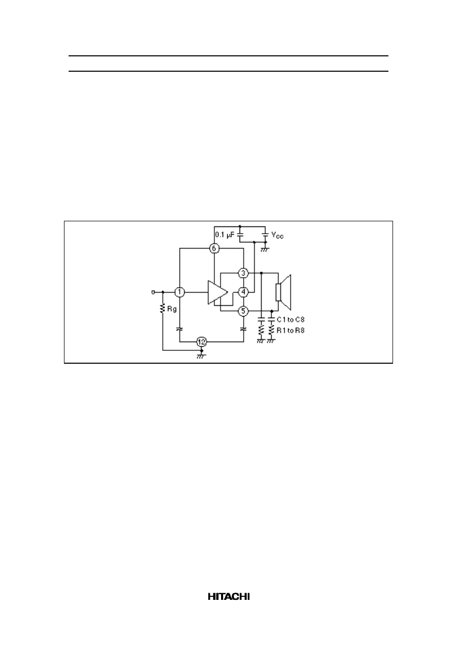
8
Point of Application Board Design
1. Notes on Application Board’s Pattern Design
•
For increasing stability, the connected line of V
CC
and OUTGND is better to be made wider and
lower impedance.
•
For increasing stability, it is better to place the capacitor between V
CC
and GND (0.1 µF) close to
IC.
•
For increasing stability, it is better to place C1 to C8 and R1 to R8, which are for stopping
oscillation, close to IC.
•
It is better to place the grounding of resistor (Rg), between input line and ground, close to INGND
(Pin 12) because if OUTGND is connected to the line between Rg and INGND, THD will become
worse due to current from OUTGND.
Figure 1 Notes on Application Board’s Pattern Design
HA13151, HA13152
9
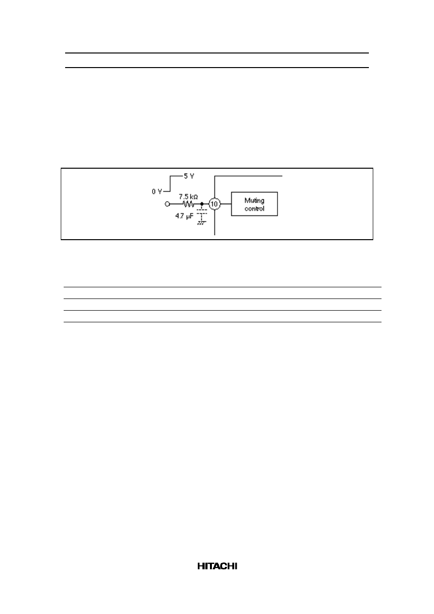
2. How to Reduce the Popping Noise by Muting Circuit
At normal operating circuit, Muting circuit operates at high speed under 1 µs.
In case popping noise becomes a problem, it is possible to reduce the popping noise by connecting
capacitor, which determines the switching time constant, between pin 10 and GND. (Following
figure 2)
We recommend value of capacitor greater then 1 µF.
Also transitional popping noise can be reduced sharply by muting before V
CC
and Standby are
ON/OFF.
Figure 2 How to use Muting Circuit
Table 1
Muting ON/OFF Time
C (µF)
ON Time
OFF Time
nothing
under 1 µs
under 1 µs
0.47
2 ms
2 ms
4.7
19 ms
19 ms
HA13151, HA13152
10
HA13151, HA13152
11
HA13151, HA13152
12
HA13151, HA13152
13
HA13151, HA13152
14
HA13151, HA13152
15

HA13151, HA13152
16
HA13151, HA13152
17
HA13151, HA13152
18
HA13151, HA13152
19
HA13151, HA13152
20
HA13151, HA13152
21
HA13151, HA13152
22
HA13151, HA13152
23
HA13151, HA13152
24
When using this document, keep the following in mind:
1. This document may, wholly or partially, be subject to change without notice.
2. All rights are reserved: No one is permitted to reproduce or duplicate, in any form, the whole or
part of this document without Hitachi’s permission.
3. Hitachi will not be held responsible for any damage to the user that may result from accidents or
any other reasons during operation of the user’s unit according to this document.
4. Circuitry and other examples described herein are meant merely to indicate the characteristics and
performance of Hitachi’s semiconductor products. Hitachi assumes no responsibility for any
intellectual property claims or other problems that may result from applications based on the
examples described herein.
5. No license is granted by implication or otherwise under any patents or other rights of any third party
or Hitachi, Ltd.
6. MEDICAL APPLICATIONS: Hitachi’s products are not authorized for use in MEDICAL
APPLICATIONS without the written consent of the appropriate officer of Hitachi’s sales company.
Such use includes, but is not limited to, use in life support systems. Buyers of Hitachi’s products
are requested to notify the relevant Hitachi sales offices when planning to use the products in
MEDICAL APPLICATIONS.
Wyszukiwarka
Podobne podstrony:
Radio Sony CDX 4170R
radio jako medium audialne
radio i sport
Instrukcja radio Gamma V PL
Bmw 01 94 Business Mid Radio Owners Manual
MPO P1 1P 152
152 System C sprezenie zewnetrzne bezprzyczepnosciowe
152
Sony Ericsson GC79, TELEFONIA, Opisy telefonów
zestawy radio
RADIO HELLO
Radio USG cw
COMPACT DISK PLAYER MODEL SONY CDX GT212 CDX GT210
MJA P1 1P 152
checklist radio tv theatre events
Heathkit Basic Electricity Course (Basic radio Pt 2) ek 2b WW
ar 156 radio 60360686 04 2001
plik (152)
więcej podobnych podstron