
Version date 03-04-06
G6ALU 20W FET PA – Construction Information
The requirement
This amplifier was designed specifically to complement the Pic-A-Star transceiver developed by Peter
Rhodes G3XJP. From the band pass filter an output of approximately –10dBm can be obtained, this requires
amplifying to a useable power level to be of use. Although developed for a specific application the design
presented here is flexible enough to be used with any low level HF signal source. Adjustment of the
attenuator value and possible removal of the first stage can accommodate a higher input power.
Circuit description
A 3 stage topology has been used requiring a nominal input of –13dBm (0.05mW) for an output of 20W at
1.8MHz falling to 16W at 30MHz (typically 25W on 80M). Typical current consumption is 2.7Amps @
13.8V, giving a stage efficiency of 53% at 20W output.
Field effect transistors have been used for the power stages, these are low cost and have so far proven to be
very robust. One failure mode that must be looked out for is excessive device dissipation; ensure that the
gate is not left “floating”. If for any reason there isn’t a DC connection the gate may rise in voltage and turn
the device on drawing excessive current leading to device failure. The devices used here are in a TO220
package which differ from switching devices in that the tab is connected to the source electrode, so in this
design are grounded by the PCB and heat sink. No insulating washers are used when bolting the devices
down to the heat sink and PCB.
To ensure a good match to the band pass filters a 5dB attenuator has been incorporated before Q1, this is
required as the input impedance will vary with frequency. When used with the Pic A Star any additional
attenuation required should be placed in the IF stage – refer to the STAR “Set up information” document.
The first gain stage follows the input attenuator, this is a simple common emitter bipolar circuit using
emitter feedback, the gain of which is set by the load impedance of T2 (200 Ohms) and that of emitter
resistor R8 (33 Ohms). These components set the voltage gain at about 8 or 18dB power gain.
Stage 2 comprises of two field effect transistors (FETs), as previously stated no negative feedback is
provided giving a stage gain of about 23dB, providing ¼ watt of drive to the output stage. FETs are
broadband devices, if driven from a constant voltage source their output can be expected to be flat across the
HF band. Unfortunately FETs have a relatively high input capacitance, in the case of the RD06HHF1s used
here it is about 27pF giving a capacitive reactance of 196 Ohms @ 30Mhz. Rather than trying to provide a
broad-band match to this reactance it is simpler just to load the gate with a resistor of much smaller value,
this does of course limit the stage gain but to me 23dB is still quite adequate! Q2 and Q3 gates are loaded
with 100R resistors, these also provide a DC path for the bias voltage.
Matched device pairs haven’t been used so separate gate bias is provided for each device, this bias is
provided from a common source; ZD1 a 5.6 volt zener diode in series with D1 giving some temperature
compensation. The driver transistors are running with a quiescent current set at 125mA each, gate load
resistors R10 and R11 are decoupled to ground via C9 and C10 so T2 “sees” a total load of 200 Ohms. The
output load of Q2 and Q3 is provided by a centre-tapped transformer wound on a BN43-1502 or Epcos
B62152A4X1 type core. As the two types have different A
L
values, different winding instructions are given
for each.

Version date 03-04-06
The output stage is very similar to that of the driver having a gain of about 21dB, the main difference being
with the output transformer arrangement and gate load resistors. This transformer consists of two cores, the
primary of each are connected in series and the outputs in parallel, this arrangement ensures that both
transistor drains are tightly coupled in anti-phase so giving good even harmonic suppression. The quiescent
current of each transistor is set to 250mA.
Construction
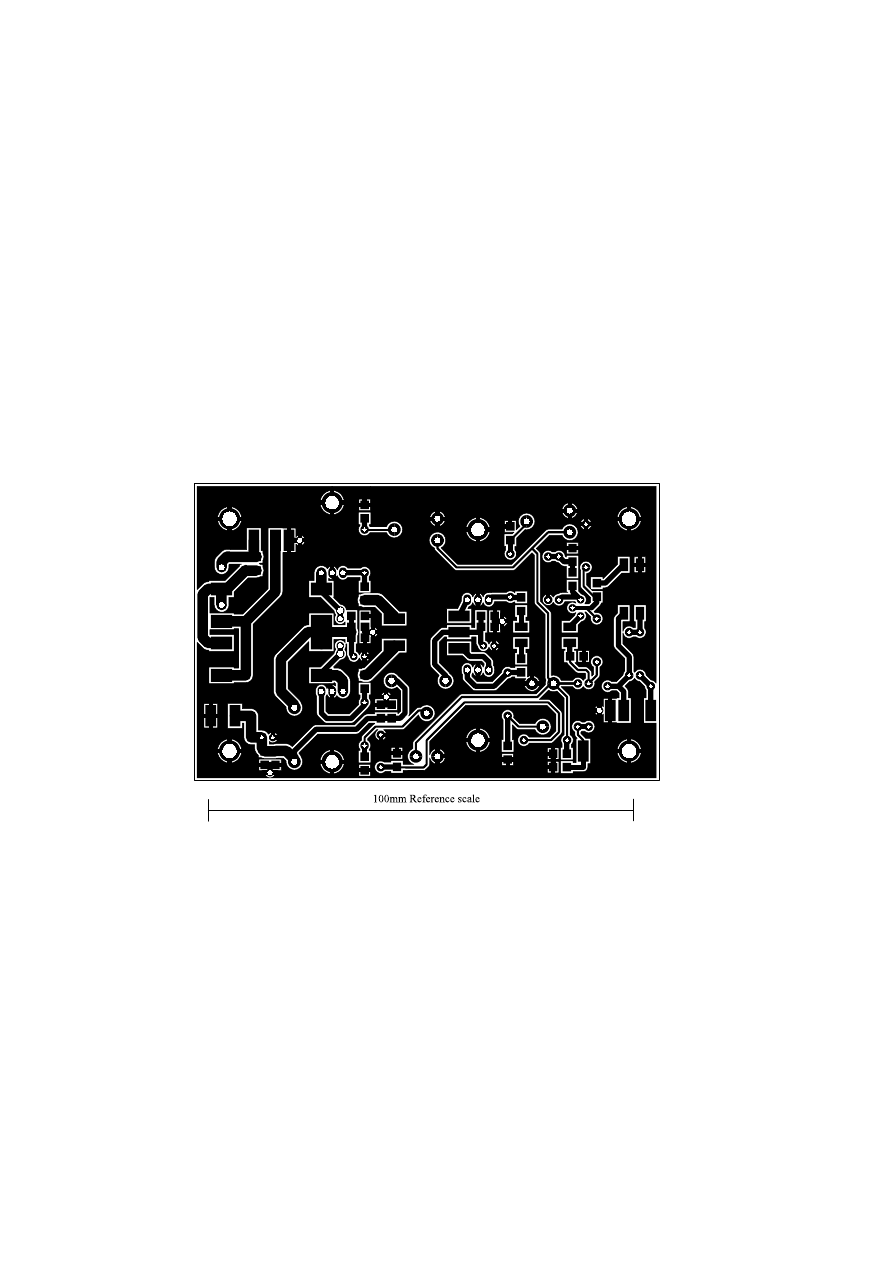
The PCB has been designed to have a continuous ground plane on the underside with connecting tracks on
the top. To enable a PCB to be manufactured using your preferred method I have included a reversed
positive plot of the top side, when plotting ensure that Acrobat isn’t resizing the plot for you by checking
with the 100mm reference provided.
As they are easier to apply and have lower parasitic inductance, surface mount capacitors have been used
where practical, in addition all transformers are surface mounted. Other components are leaded types and
pass through the PCB, note that anywhere a grounded lead passes through the PCB it should be soldered top
and bottom, in addition there are 6 through board links that need soldering both sides. All non-grounded
leads which pass through the board should have the ground plane relieved on the underside.
Transformer winding - All transformers are simple to wind, wire diameter for transformers T1 and T2 isn’t
critical. For T3 don’t be tempted to greatly increase the diameter of wire although the core holes would
allow it, using a wire significantly thicker increases its self capacitance affecting the transformer wide band
performance.
The one turn primary of T4 and T5 can be made from a piece of braid removed from RG58 or similar coax,
for the secondary winding use PVC covered hook up wire. Use the heaviest type that will pass through the
cores.
As previously noted no insulating washers are used between the heat sink, transistors and PCB. A direct
ground connection must be made between the PCB and heat sink, grounding for the Fets is mainly made via
their tabs. Two options are provided for output HF compensation, the low cost route is to use two 1nF
surface mount ceramic capacitors but due to their questionable suitability (due to max current handling)
provision has been made for a 2n2 silver mica part. So far though there are no reported failings of ceramic
capacitors, the choice is yours.
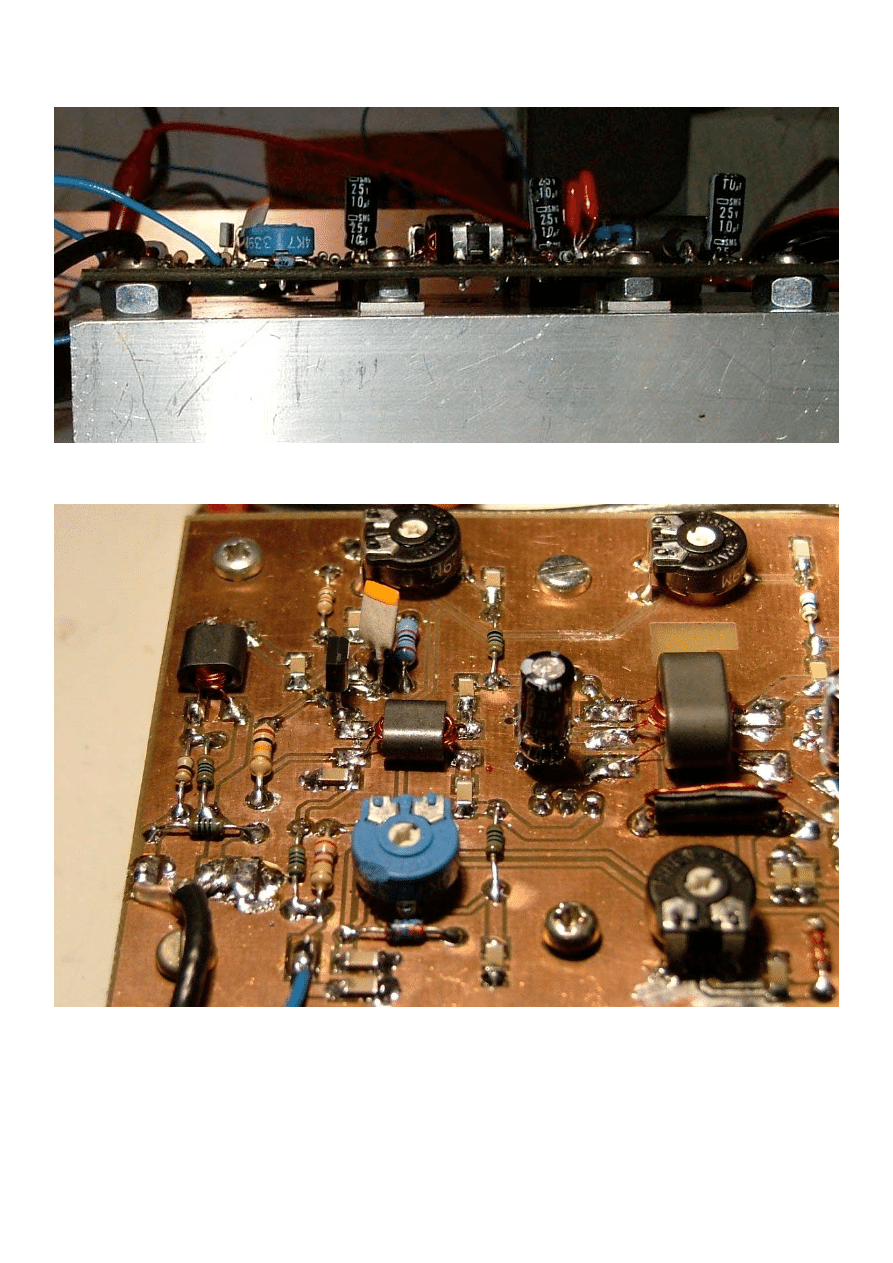
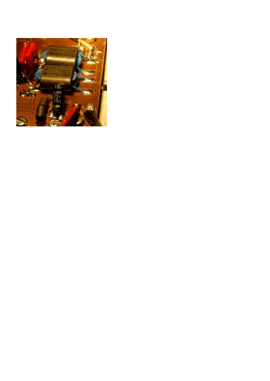
The following pictures are of the prototype, some component positions have changed with the published
version.
Version date 03-04-06
Method I used to space PCB from heatsink, note the carefully chosen nuts and washers used as spacers.
Picture showing component mounting methods and a melted preset.. it was the prototype!
Version date 03-04-06
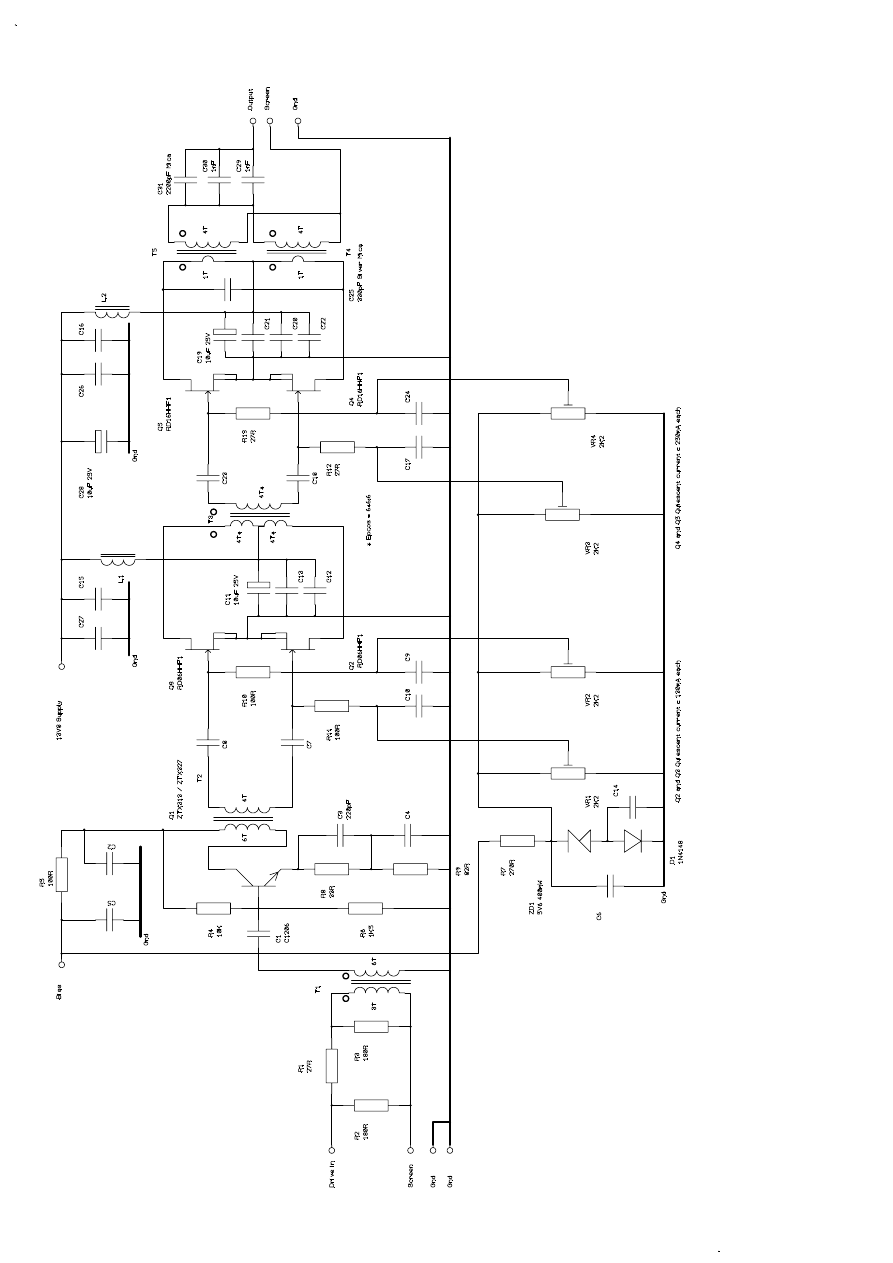
Output transformer mounting detail.
Testing and alignment
Before applying power check and make sure there are no bridges between any pads and the ground plane.
Turn all bias presets anticlockwise (lowest bias voltage). Momentarily apply a supply to the 13V8 terminal
and check current drawn is practically zero; C28 will draw initial charging current.
Apply supply to the Bias input and separately to the 13V8 input via an ammeter capable of reading 1 Amp,
connect a power meter and 50-Ohm dummy load to the output. Adjust VR1 for a quiescent current of
125mA, VR2 for an increase of 125mA (250mA total), VR3 for an increase of 250mA (500mA total) and
finally VR4 for another 250mA increase giving 750mA total quiescent current. Bias adjustment will be
sensitive but actual values achieved aren’t critical. At this stage there shouldn’t be any RF power appearing
at the dummy load!
Disconnect power, attach to the band pass filter transmit output of the STAR and apply power. Select 80M
and adjust the drive level to a low level, with key down slowly increase the drive and monitor the output
level. If an oscilloscope is available monitor the output waveform, it should be easy to achieve an output of
20W on 80M before the output becomes distorted. Repeat drive adjustment for all bands.
In Use
Note that the input and output circuits are “floating”, in normal use the coaxial screen connection will be
linked to the PCB ground pad. This facility has been provided for situations where a specific cabinet
construction generates a ground loop, a floating input or output may “break” the loop.
No output filter is provided, the amplifier still has considerable gain in to the VHF region so must be used
with an effective low pass filter, typically the second harmonic is 40dB down on carrier but third harmonic
only 25dB down.
When used with a STAR the bias supply is provided directly by the timer board (12V Tx PA bias) and 13V8
terminal left permanently connected to supply, the transistors were developed for use in mobile equipment
so can be safely supplied with higher than the normal shack voltage of 13.8V. For an increase in output up to
14.5V may be used safely.

Version date 03-04-06
Component Sources
Q1 is specified as a ZTX327 or ZTX313, both of which are now obsolete! An alternative may be the
MPSH10 or indeed any other RF transistor of suitable current and frequency rating, watch the pin outs
though and adjust C3 to compensate the HF end of band.
The FET devices were obtained from European Microwave Components, contact details:
European Microwave Components Ltd.
36 Priors Way Business Park,
Coggeshall,
Essex.
United Kingdom.
CO6 1TW
Web
http://www.emc.uk.com
and email
sales@emc.uk.com
, note that their minimum order charge before
VAT is £25, the value of transistors used in this design total about £8.00!
Ferrite cores can be obtained from any of the normal vendors; no doubt substitutions can be made especially
with T1 – T3 whose characteristics aren’t critical.
Change log:
28-04-05
Corrected input power requirements following robustness test
Changed harmonic output level
Added note about PCB grounding
Added note on through board links
Added notes on transformer construction
02-05-05
Corrected value of C3 in parts list to 220pF
03-04-06
Input attenuator changed from 10dB to 5dB, additional attenuation now placed in IF stage.
R2 and R3 were 100R, now 180R. R1 was 68R now 27R

Version date 03-04-06
Quantity Component reference
Description
Notes
Function
23
C1, 2, 4, 5, 6, 7, 8, 9, 10,
12, 13, 14, 15, 16, 17,
18, 20, 21, 22, 23, 24,
26, 27
100nF 1206 SM
Coupling - decoupling
3
C11, 19, 28
10uF 25V PC
electrolytic
LF decoupling
1
C25
330pF Silver Mica >
100V
Can be made up of multiple capacitors
HF frequency compensation
of T4 & T5
2
C29, 30
1nF 1206 SM
Not used if C31 fitted, see text
LF frequency compensation
for T4 & T5
1
C3
220pF 1206 SM
HF peaking for Q1
1
C31
2200pF Silver Mica Not used if C29 & 30 fitted, see text
LF frequency compensation
for T4 & T5
1
D1
1N4148
Partial temperature
compensation for bias supply
1
ZD1
5V6 400mW
Bias voltage regulation
1
Q1
ZTX313, ZTX327
First stage amplification
2
Q2, Q3
RD06HHF1
See text
Second stage amplification
2
Q4, Q5
RD16HHF1
See text
Third stage amplification
3
R5, R10, R11
100R
R5 decoupling, R10 & R11
load for 1st stage amplifier
and gate reactance swamp
resistors
3
R1, R12, R13
27R
R1 part of input attenuator.
R12, 13 Gate reactance
swamping resistors for Q4
and 5
1
R4
10K
Part of Q1 bias
1
R6
1K5
Part of Q1 bias
1
R7
270R
Resistor will dissipate about 0.3W so miniature 0.6W MF
recommended
Series resistor for FET bias
supply
2
R2, R3
180R
Input attenuator
1
R8
33R
Q1 gain setting
1
R9
82R
Q1 emitter resistor
Unless otherwise stated all resistors 1/8 watt or higher , 5%
tolerance or better
4
VR1, VR2, VR3, VR4
2K2 Horizontal
preset
Q3-6 gate bias setting
1
L1
2* type 43 beads
2 passes of 0.25mm enamelled copper wire through 2 type 43
beads - see photos
Supply decoupling
1
L2
2* type 43 beads
1 pass of 1.25mm tinned copper wire through 2 type 43 beads -
see photos
Supply decoupling
1
T1
BN43-2402
Primary 3 turns, secondary 6 turns of 0.25mm enamelled
copper wire wound on to BN43-2402 core
1
T2
BN43-2402
Primary 6 turns, secondary 4 turns of 0.25mm enamelled
copper wire wound on to BN43-2402 core
1
T3
BN43-1502 or
Siemens (Epcos)
B62152A4X1
Primary 8 turns centre tapped (I.E. 4+4), secondary 4 turns
0.25mm enamelled copper wire wound on type BN43-1502 or
for Epcos B62152A4X1 core, 12 turns centre tapped primary
with 6 turn secondary.
2
T4, T5
BN43-202
Primary 1 turn of braid removed from RG58 cable or similar,
secondary 4 turns of PVC covered hook up wire wound on
BN43-202 core - see photo.
20W HF PA Component list
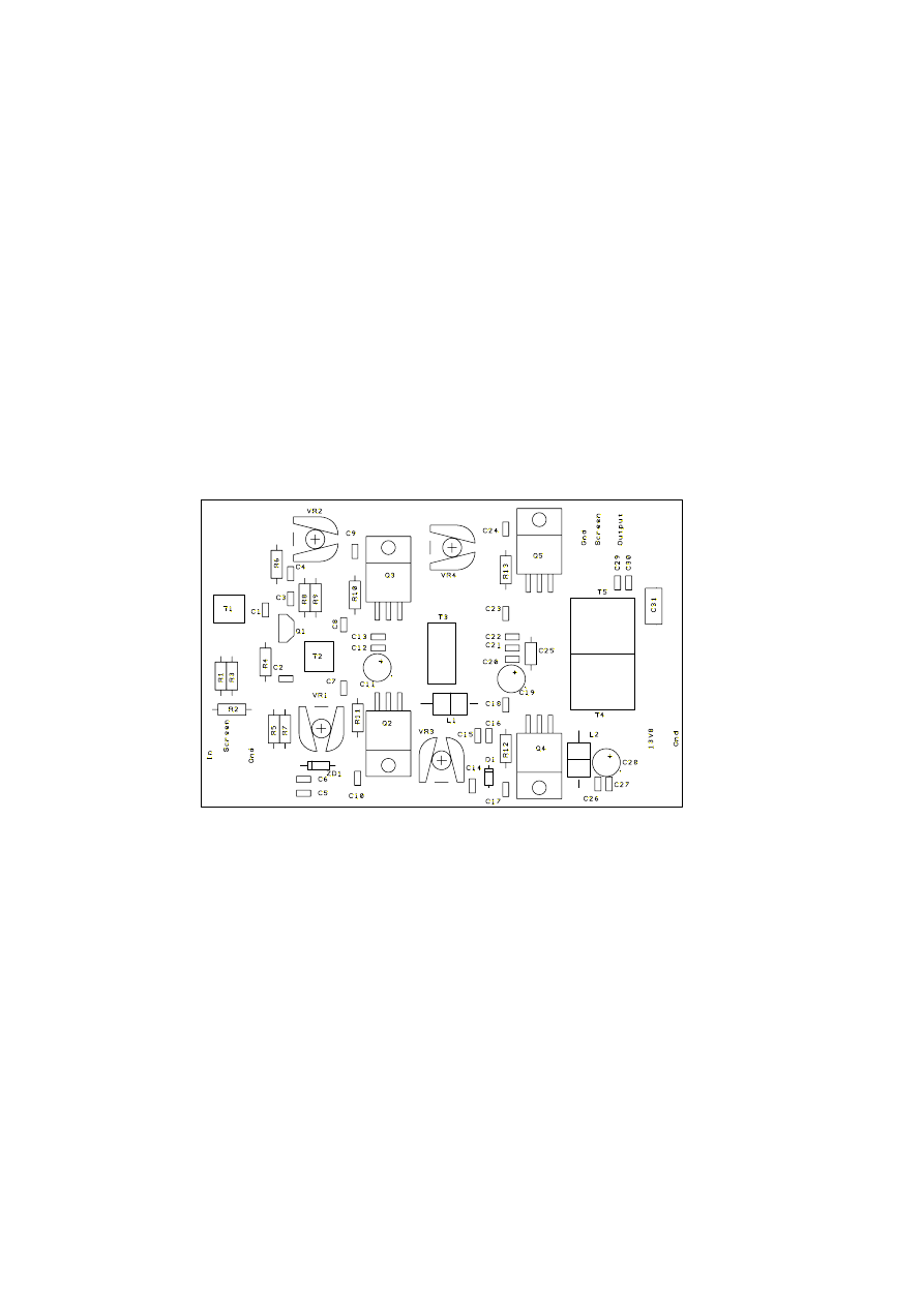
All unmarked capacitors
are 100nF S/M types
Wyszukiwarka
Podobne podstrony:
Samba Pa Ti v2
Lab1 PA podstawy PSCAD v2
Lab1 PA podstawy PSCAD v2
Wyklad 9 Post HF
BUD»ET PAĐSTWA
DTC v2
wyklad 1 hf
Elektro (v2) poprawka
l1213 r iMiBM lakei v2
logika rozw zadan v2
poprawkowe, MAD ep 13 02 2002 v2
DSC PC5010 v2 0 obs lcd
constructionands033261mbp
87 Dz U 08 25 150 Prawo ochrony środowiska v2
HF 91110 80 Amp Inverter Arc Welder
więcej podobnych podstron