TDA7261
25W MONO AMPLIFIER WITH MUTE/ST-BY
WIDE SUPPLY VOLTAGE RANGE (UP TO
50V ABS MAX.)
SPLIT SUPPLY
HIGH OUTPUT POWER:
25W @ THD =10%, R
L
= 8
Ω
, V
S
= +20V
NO POP AT TURN-ON/OFF
MUTE (POP FREE)
STAND-BY FEATURE (LOW I
Q
)
FEW EXTERNAL COMPONENTS
SHORT CIRCUIT PROTECTION
THERMAL OVERLOAD PROTECTION
DESCRIPTION
The TDA7261 is class AB Audio power amplifier
assembled in the Multiwatt package, specially de-
signed for high quality sound application in mono
TV chassis.
September 2003
®
Multiwatt 8
ORDERING NUMBER: TDA7261
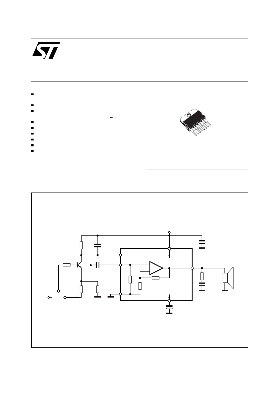
+5V
18K
15K
IN
1
µ
F
15K
1
µ
F
MUTE/
ST-BY
GND
4.7
Ω
100nF
OUT
1000
µ
F
1000
µ
F
+V
S
2
4
6
7
5
3
+
-
D94AU088
RL
+V
S
-V
S
µ
P
Figure 1: Typical Application Circuit
1/9
ABSOLUTE MAXIMUM RATINGS
Symbol
Parameter
Value
Unit
V
S
DC Supply Voltage
50
V
I
O
Output Peak Current (internally limited)
4.5
A
P
tot
Power Dissipation T
case
= 70
°
C
30
W
T
stg
, T
j
Storage and Junction Temperature
-40 to +150
°
C
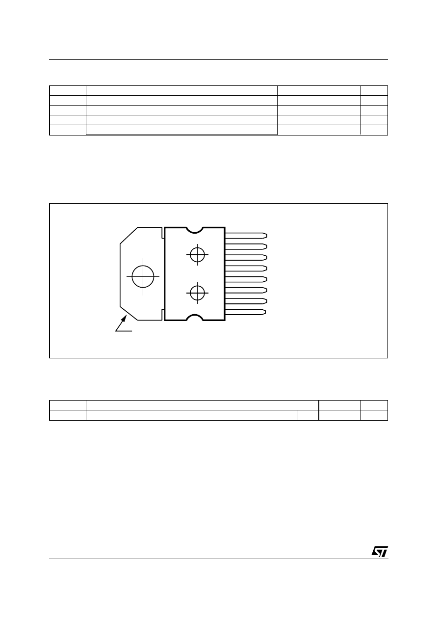
1
2
3
4
5
6
7
D94AU090
8
N.C.
GND
IN
-V
S
MUTE/ST-BY
OUTPUT
+V
S
N.C.
Tab connected to pin 5
PIN CONNECTION (Top view)
THERMAL DATA
Symbol
Description
Value
Unit
R
th j-case
Thermal Resistance Junction-case
Max
2.5
°
C/W
TDA7261
2/9
ELECTRICAL CHARACTERISTICS (Refer to the test circuit, V
S
+ 20V; R
L
= 8
Ω
; R
s
=50
Ω
;
f = 1KHz; T
amb
= 25
°
C, unless otherwise specified.)
Symbol
Parameter
Test Condition
Min.
Typ.
Max.
Unit
V
S
Supply Range
+5
+22.5
V
I
q
Total Quiescent Current
30
mA
P
O
Music Output Power (*)
THD = 10%; R
L
= 8
Ω
;
V
S
+ 28.5V;
32
W
P
O
Output Power
THD = 10%
R
L
= 8
Ω
;
V
S
+ 16V; R
L
= 4
Ω
20
25
25
W
W
THD = 1%
R
L
= 8
Ω
;
V
S
+ 16V; R
L
= 4
Ω
20
20
W
W
THD
Total Harmonic Distortion
R
L
= 8
Ω
; P
O
= 1W; f = 1KHz
0.02
%
R
L
= 8
Ω
;
P
O
= 0.1 to 15W;
f = 100Hz to 15KHz
0.5
%
R
L
= 4
Ω
; P
O
= 1W; f = 1KHz
0.03
%
R
L
= 4
Ω
; V
S
+ 16V;
P
O
= 0.1 to 12W;
f = 100Hz to 15KHz
1
%
SR
Slew Rate
10
V/
µ
s
G
V
Closed Loop Voltage Gain
29
30
31
dB
∆
G
V
Voltage Gain Matching
0.2
dB
e
N
Total Input Noise
A Curve
f = 20Hz to 22KHz
2.5
3.5
8
µ
V
µ
V
R
i
Input Resistance
15
20
K
Ω
SVR
Supply Voltage Rejection
fr = 100Hz; Vripple = 0.5V
RMS
60
dB
T
j
Thermal Shut-down
Junction Temperature
145
°
C
MUTE FUNCTION [ref: +V
S
]
VT
MUTE
Mute / Play Threshold
-7
-6
-5
V
A
M
Mute Attenuation
60
90
dB
STAND-BY FUNCTION [ref: +V
S
]
VT
ST-BY
Stand-by / Mute Threshold
-3.5
-2.5
-1.5
V
A
ST-BY
Stand-by Attenuation
110
dB
I
q ST-BY
Quiescent Current @ Stand-by
3
mA
Note :
(*) FULL POWER up to. V
S
=
±
22.5V with R
L
= 8
Ω
and V
S
=
±
16V with R
L
= 4
Ω
MUSIC POWER is the maximal power which the amplifier is capable of producing across the rated load resistance (regardless of non linearity)
1 sec after the application of a sinusoidal input signal of frequency 1KHz.
TDA7261
3/9
COMPONENTS
RECOMMENDED
VALUE
PURPOSE
LARGER THAN
RECOMMENDED VALUE
SMALLER THAN
RECOMMENDED VALUE
R1
10K
Ω
Mute Circuit
Increase of Dz
Biasing Current
R2
15K
Ω
Mute Circuit
V
pin
# 4 Shifted Downward
V
pin
# 4 Shifted Upward
R3
18K
Ω
Mute Circuit
V
pin
# 4 Shifted Upward
V
pin
# 4 Shifted Downward
R4
15K
Ω
Mute Circuit
V
pin
# 4 Shifted Upward
V
pin
# 4 Shifted Downward
R5
4.7
Ω
Frequency Stability
Danger of Oscillations
Danger of Oscillations
C1
1
µ
F
Input DC
Decoupling
Higher Low Frequency
Cutoff
C2
1
µ
F
St-By/Mute Time
Constant
Larger On/Off Time
Smaller On/Of Time
C3, C5
1000
µ
F
Supply Voltage
Bypass
Danger of Oscillations
C4, C6
0.1
µ
F
Supply Voltage
Bypass
Danger of Oscillations
C7
0.1
µ
F
Frequency Stability
Dz
5.1V
Mute Circuit
Q1
BC107
Mute Circuit
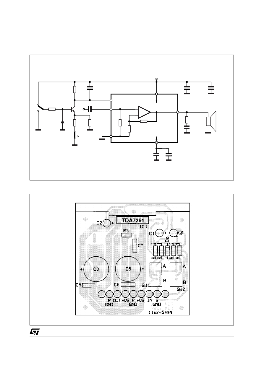
APPLICATIONS SUGGESTION
(Demo Board Schematic)
The recommended values of the external compo-
nents are those shown on the demo board sche-
matic. Different values can be used: the following
table can help the designer.
MUTE, STAND-BY TRUTH TABLE
SW1
SW2
A
A
STAND-BY
A
B
STAND-BY
B
B
MUTE
B
A
PLAY
TDA7261
4/9
R3
18K
IN
C1 1
µ
F
MUTE/
ST-BY
GND
R5
4.7
Ω
C7
100nF
OUT
C5
1000
µ
F
C3
1000
µ
F
+V
S
2
4
6
7
5
3
+
-
D94AU089A
RL
+V
S
-V
S
SW1
R1
DZ
Q1
R4
15K
R2
15K
C2
1
µ
F
SW2
C4
100nF
C6
100nF
ST-BY
MUTE
Figure 2: Demo Board Schematic
Figure 3: P.C. Board And Component Layout of the Demo Board Schematic (1:1 Scale)
TDA7261
5/9
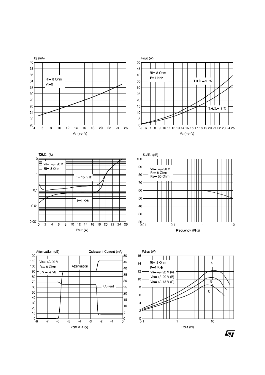
Figure 7: Supply Voltage Rejection vs. Fequency
Figure 6: Distortion vs. Output Power
Figure 4: Quiescent Current vs. Supply Voltage
Figure 5: Output Power vs Supply Voltage
Figure 8: Attenuation & Total Quiescent Current
vs. Vpin4 Voltage
Figure 9: Power Dissipation vs. Output Power
TDA7261
6/9
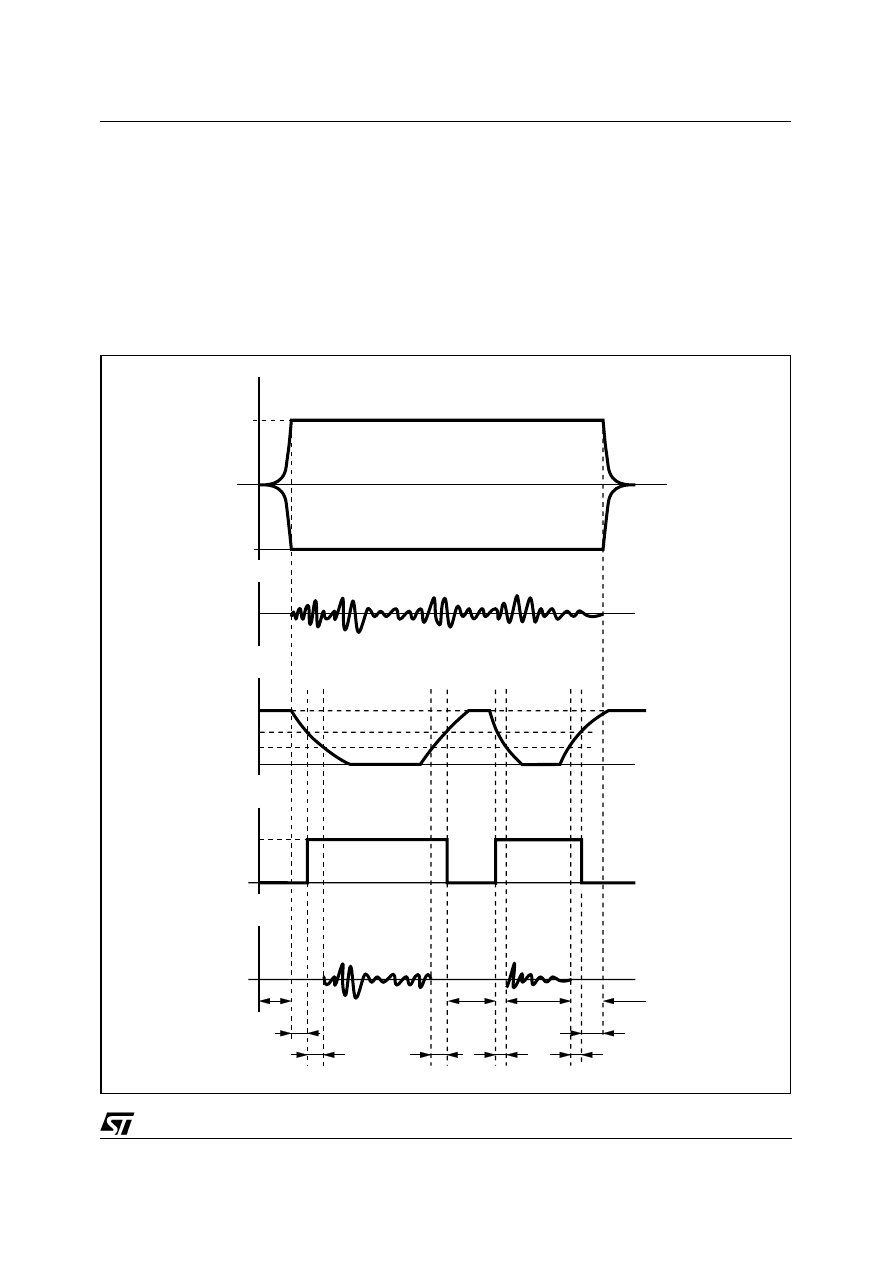
MUTE STAND-BY FUNCTION
The pin 4 (MUTE/STAND-BY) controls the ampli-
fier status by two different theresholds, referred to
+V
S
.
- When V
pin4
higher than = +V
S
- 2.5V the
amplifier is in Stand-by mode and the final
stage generators are off.
- When V
pin4
is between +V
S
- 2.5V and +V
S
- 6V the final stage current generators are
switched on and the amplifier is in mute
mode.
- When V
pin4
is lower than +V
S
- 6V the am-
plifier is play mode.
t
OFF
STDBY
MUTE
MUTE
MUTE
MUTE
PLAY
STDBY
PLAY
OFF
STDBY
20
+V
S
(V)
-20
-V
S
V
IN
(mV)
Vpin4
(V)
V
S
V
S
-2.5
V
S-
6
V
S
-10
I
q
(mA)
0
VOUT
(V)
D94AU084
Figure 10
TDA7261
7/9
Multiwatt8 (Floating)
*
DIM.
mm
inch
MIN.
TYP.
MAX.
MIN.
TYP.
MAX.
A
5
0.197
B
2.65
0.104
C
1.6
0.063
E
0.49
0.55
0.019
0.022
F
0.78
0.85
0.030
0.033
F1
0.68
0.75
0.027
0.029
G
2.40
2.54
2.68
0.094
0.10
0.105
G1
17.64
17.78
17.92
0.69
0.70
0.71
H1
19.6
0.772
H2
20.2
0.795
L
20.35
20.65
0.80
0.81
L2
17.05
17.20
17.35
0.67
0.68
0.68
L3
17.25
17.5
17.75
0.679
0.689
0.699
L4
10.3
10.7
10.9
0.406
0.421
0.429
L5
L5*
15.45
15.05
15.75
15.35
0.61
0.59
0.62
0.60
L7
2.65
2.9
0.104
0.114
S
1.9
2.6
0.075
0.102
S1
1.9
2.6
0.075
0.102
U
0.40
0.55
0.015
0.022
Z
0.70
0.85
0.028
0.034
Dia1
3.65
3.85
0.144
0.152
L5 = with wedged frame std.
L5* = with wedged frame anchor holes.
OUTLINE AND
MECHANICAL DATA
TDA7261
8/9

Information furnished is believed to be accurate and reliable. However, STMicroelectronics assumes no responsibility for the consequences
of use of such information nor for any infringement of patents or other rights of third parties which may result from its use. No license is
granted by implication or otherwise under any patent or patent rights of STMicroelectronics. Specifications mentioned in this publication are
subject to change without notice. This publication supersedes and replaces all information previously supplied. STMicroelectronics products
are not authorized for use as critical components in life support devices or systems without express written approval of STMicroelectronics.
The ST logo is a registered trademark of STMicroelectronics.
All other names are the property of their respective owners
© 2003 STMicroelectronics - All rights reserved
STMicroelectronics GROUP OF COMPANIES
Australia – Belgium - Brazil - Canada - China – Czech Republic - Finland - France - Germany - Hong Kong - India - Israel - Italy - Japan -
Malaysia - Malta - Morocco - Singapore - Spain - Sweden - Switzerland - United Kingdom - United States
www.st.com
TDA7261
9/9
Wyszukiwarka
Podobne podstrony:
TDA7266M STMicroelectronics elenota pl
TDA7266S STMicroelectronics elenota pl
TDA7266D STMicroelectronics elenota pl
TDA7266L STMicroelectronics elenota pl
TDA7265 STMicroelectronics elenota pl
TDA7388 STMicroelectronics elenota pl
TDA7383 STMicroelectronics elenota pl
TDA7566 STMicroelectronics elenota pl
TDA7850 STMicroelectronics elenota pl
TDA7490LSA STMicroelectronics elenota pl
TDA1908 STMicroelectronics elenota pl (1)
TDA7233 STMicroelectronics elenota pl
TDA7231A STMicroelectronics elenota pl
TDA7360 STMicroelectronics elenota pl
TDA7386 STMicroelectronics elenota pl (2)
TDA7385 STMicroelectronics elenota pl
TDA7490SA STMicroelectronics elenota pl
więcej podobnych podstron