TDA7266L
5W MONO BRIDGE AMPLIFIER
WIDE SUPPLY VOLTAGE RANGE (3.5V-18V)
MINIMUM EXTERNAL COMPONENTS
– NO SVR CAPACITOR
– NO BOOTSTRAP
– NO BOUCHEROT CELLS
– INTERNALLY FIXED GAIN
STAND-BY & MUTE FUNCTIONS
SHORT CIRCUIT PROTECTION
THERMAL OVERLOAD PROTECTION
DESCRIPTION
The TDA7266L is a mono bridge amplifier spe-
cially designed for TV and Portable Radio appli-
cations.
February 2001
®
10
9
7
Vref
(ST-BY)
ST-BY
4
IN1
5V
S
1
S
2
C
1
0.22
µ
F
C
2
C
4
R
1
R
2
VCC
8
D99AU1039A
+
-
-
+
OUT+
OUT-
MUTE
MUTE
3
5
6
S-GND
PW-GND
C5
470
µ
F
C6
100nF
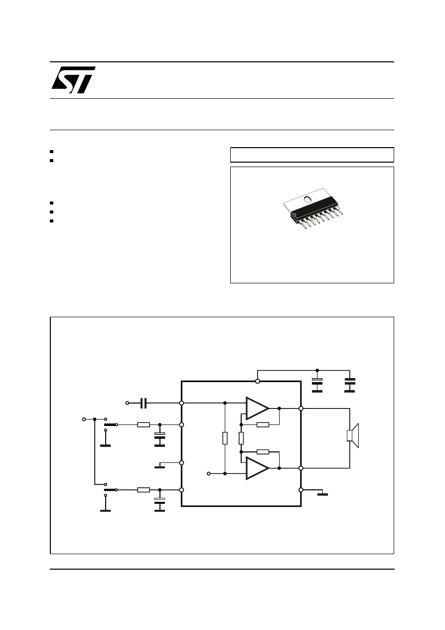
BLOCK AND APPLICATION DIAGRAM
SIP10
ORDERING NUMBER: TDA7266L
TECHNOLOGY BI20II
1/7
ELECTRICAL CHARACTERISTICS (V
CC
= 11V, R
L
= 8
Ω
, f = 1kHz, T
amb
= 25
°
C unless otherwise
specified.)
Symbol
Parameter
Test Condition
Min.
Typ.
Max.
Unit
V
CC
Supply Range
3.5
10
18
V
I
q
Total Quiescent Current
35
50
mA
V
OS
Output Offset Voltage
120
mV
P
O
Output Power
THD = 10%
5.5
7
W
THD
Total Harmonic Distortion
P
O
= 1W
0.05
0.2
%
P
O
= 0.1W to 2W
f = 100Hz to 15kHz
1
%
SVR
Supply Voltage Rejection
f = 100Hz VR = 0.5V
40
50
dB
A
MUTE
Mute Attenuation
60
80
dB
T
W
Thermal Threshold
150
°
C
G
V
Closed Loop Voltage Gain
32
dB
R
i
Input Resistance
31
33
K
Ω
VT
MUTE
Mute Threshold
for V
CC
> 6.4V; V
O
= -30dB
for V
CC
< 6.4V; V
O
= -30dB
2.3
V
CC
/2
-1
2.9
V
CC
/2
-0.75
4.1
V
CC
/2
-0.5
V
V
1
2
3
4
5
6
7
8
V
CC
IN
S-GND
PW-GND
ST-BY
MUTE
N.C.
N.C.
9
10
OUT-
OUT+
D99AU1040A
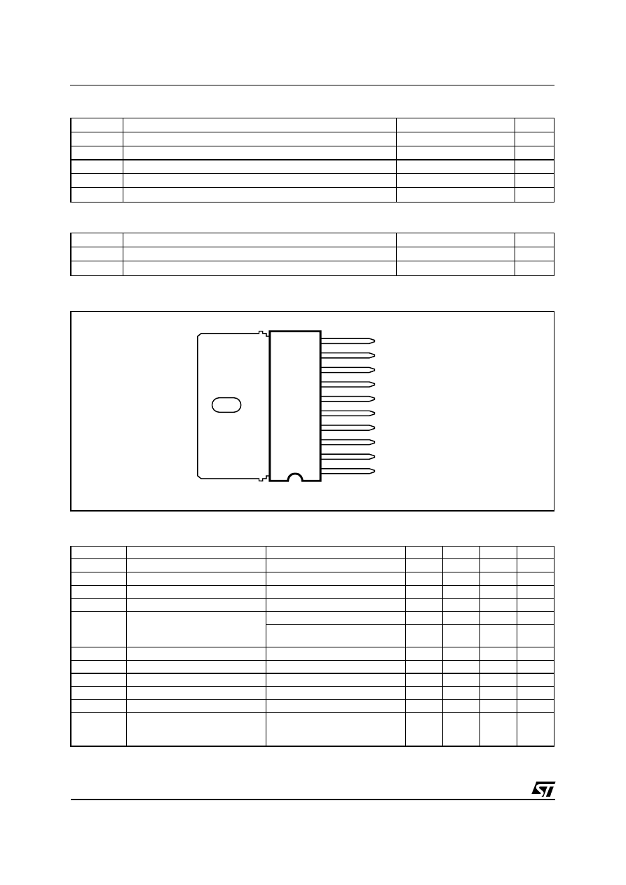
PIN CONNECTION (Top view)
ABSOLUTE MAXIMUM RATINGS
Symbol
Parameter
Value
Unit
V
S
Supply Voltage
20
V
I
O
Output Peak Current (internally limited)
2
A
P
tot
Total Power Dissipation (T
case
= 70
°
C)
10
W
T
op
Operating Temperature
0 to 70
°
C
T
stg
, T
j
Storage and Junction Temperature
-40 to +150
°
C
THERMAL DATA
Symbol
Description
Value
Unit
R
th j-case
Thermal Resistance Junction to case
8
°
C/W
R
th j-amb
Thermal Resistance Junction to ambient
70
°
C/W
TDA7266L
2/7
ELECTRICAL CHARACTERISTICS (Continued)
Symbol
Parameter
Test Condition
Min.
Typ.
Max.
Unit
VT
ST-BY
St-by Threshold
0.8
1.3
1.8
V
I
ST-BY
ST-BY current V6 = GND
100
µ
A
e
N
Total Output Noise Voltage
A curve
f = 20Hz to 20kHz
150
µ
V
APPLICATION SUGGESTION
STAND-BY AND MUTE FUNCTIONS
(A) Microprocessor Application
In order to avoid annoying "Pop-Noise" during
Turn-On/Off transients, it is necessary to guaran-
tee the right St-by and mute signals sequence.
It is quite simple to obtain this function using a mi-
croprocessor (Fig. 1 and 2).
At first St-by signal (from mP) goes high and the
voltage across the St-by terminal (Pin 7) starts to
increase exponentially. The external RC network
is intended to turn-on slowly the biasing circuits of
the amplifier, this to avoid "POP" and "CLICK" on
the outputs.
When this voltage reaches the St-by threshold
level, the amplifier is switched-on and the external
capacitors in series to the input terminals (C3,
C5) start to charge.
It’s necessary to mantain the mute signal low until
the capacitors are fully charged, this to avoid that
the device goes in play mode causing a loud "Pop
Noise" on the speakers.
A delay of 100-200ms between St-by and mute
signals is suitable for a proper operation.
(B) Low Cost Application
In low cost applications where the
µ
P is not pre-
sent, the suggested circuit is shown in fig.3.
The St-by and mute terminals are tied together
and they are connected to the supply line via an
external voltage divider.
The device is switched-on/off from the supply line
and the external capacitor C4 is intended to delay
the St-by and mute threshold exceeding, avoiding
"Popping" problems.
+V
S
(V)
V
IN
(mV)
V
ST-BY
pin 7
I
q
(mA)
ST-BY
MUTE
PLAY
MUTE
ST-BY
+18
1.8
0.8
V
MUTE
pin 6
4.1
2.3
OFF
OFF
D96AU259
V
OUT
(V)
2.9
1.3
Figure 1: Microprocessor Driving Signals.
TDA7266L
3/7
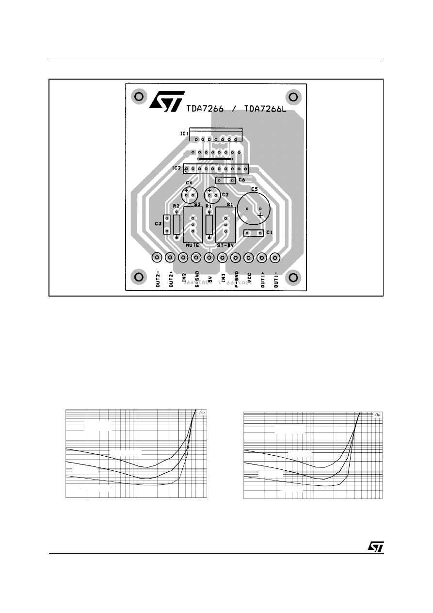
Figure 2: PCB and Component Layout of the Application Diagram
The PC board layout offers compatibility to TDA7266S, TDA7266, TDA7297, (the BTL power amplifiers
in Multiwatt 15 package).
0 .0 1 0
0 .1
1
1 0
0 .1
1
1 0
V cc = 11 V
R l = 8 ohm
f = 1 5 K H z
f = 5 K H z
f = 1 K H z
P ou t (W )
TH D (% )
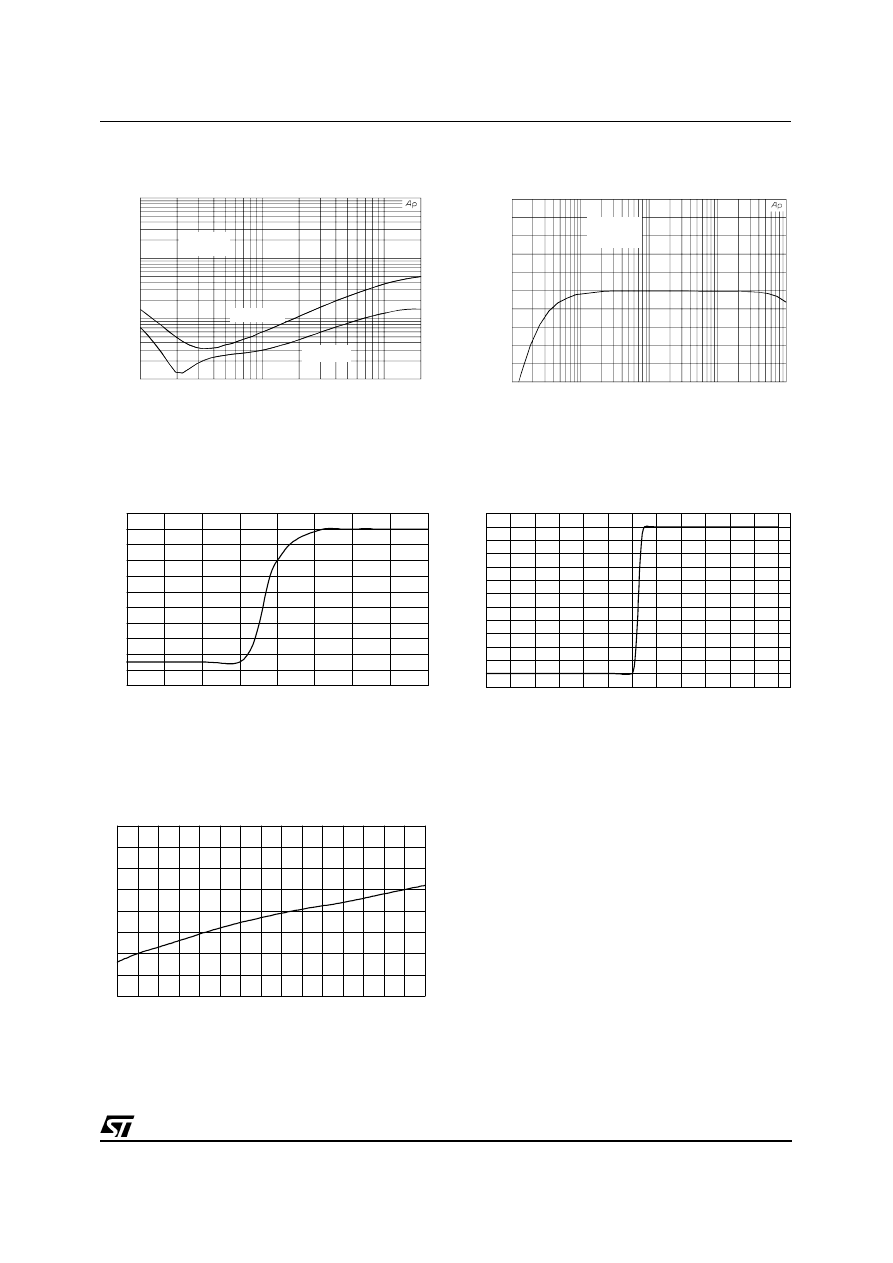
Figure 3: Distortion vs Output Power
0.0 10
0.1
1
10
0.1
1
10
T H D (% )
V cc = 9V
R l= 8 o h m
f = 1 5K H z
f = 5 K H z
f = 1 K H z
P o u t (W )
Figure 4: Distortion vs Output Power
TDA7266L
4/7
0.0 10
0.1
1
10
100
1k
10k
20k
THD(%)
V cc = 11 V
R l = 8 o hm
P ou t = 100 m W
P ou t = 2W
freque ncy (Hz)
Figure 5: Distortion vs Frequency
-5.000
-4.000
-3.000
-2.000
-1.000
0.0
1.0000
2.0000
3.0000
4.0000
5.0000
10
100
1k
10k
100k
Level(dBr)
Vcc = 11V
Rl = 8 ohm
Pout = 1W
frequency (Hz)
Figure 6: Gain vs Frequency
1
1.5
2
2.5
3
3.5
4
4.5
5
0
10
-10
-20
-30
-40
-50
-60
-70
-80
-90
-100
Attenuation (dB)
Vpin.6(V)
Figure 7: Mute Attenuation vs. V pin.6
0
0.2
0.4
0.6
0.8
1
1.2
1.4
1.6
1.8
2
2.2
2.4
0
10
-10
-20
-30
-40
-50
-60
-70
-80
-90
-100
-110
-120
Attenuation (dB)
Vpin.7 (V)
Figure 8: Stand-By Attenuation vs Vpin.7
3
4
5
6
7
8
9
10
11
12
13
14
15
16
17
18
30
35
40
45
50
55
60
65
70
Iq (mA)
Vsupply(V)
Figure 9: Quiescent Current vs. Supply Voltage
TDA7266L
5/7
SIP10
DIM.
mm
inch
MIN.
TYP.
MAX.
MIN.
TYP.
MAX.
A
7.1
0.280
a1
2.7
3
0.106
0.118
B
24.8
0.976
b1
0.5
0.020
b3
0.85
1.6
0.033
0.063
C
3.3
0.130
c1
0.43
0.017
c2
1.32
0.052
D
23.7
0.933
d1
14.5
0.571
e
2.54
0.100
e3
22.86
0.900
L
3.1
0.122
L1
3
0.118
L2
17.6
0.693
L3
0.25
0.010
L4
0.254
0.010
M
3.2
0.126
N
1
0.039
P
0.15
0.006
D
N
M
L1
1
1
0
d1
L3
L2
La
1
e3
b1
B
e
c
1
A
c2
C
P
L4
SIP10
b3
OUTLINE AND
MECHANICAL DATA
TDA7266L
6/7

Information furnished is believed to be accurate and reliable. However, STMicroelectronics assumes no responsibility for the consequences
of use of such information nor for any infringement of patents or other rights of third parties which may result from its use. No license is
granted by implication or otherwise under any patent or patent rights of STMicroelectronics. Specification mentioned in this publication are
subject to change without notice. This publication supersedes and replaces all information previously supplied. STMicroelectronics products
are not authorized for use as critical components in life support devices or systems without express written approval of STMicroelectronics.
The ST logo is a registered trademark of STMicroelectronics
©2001 STMicroelectronics – Printed in Italy – All Rights Reserved
STMicroelectronics GROUP OF COMPANIES
Australia - Brazil - Canada - China - France - Germany - Italy - Japan - Korea - Malaysia - Malta - Mexico - Morocco - The Netherlands -
Singapore - Spain - Sweden - Switzerland - Taiwan - Thailand - United Kingdom - U.S.A.
http://www.st.com
TDA7266L
7/7
Wyszukiwarka
Podobne podstrony:
TDA7266M STMicroelectronics elenota pl
TDA7266S STMicroelectronics elenota pl
TDA7266D STMicroelectronics elenota pl
TDA7261 STMicroelectronics elenota pl
TDA7265 STMicroelectronics elenota pl
TDA7388 STMicroelectronics elenota pl
TDA7383 STMicroelectronics elenota pl
TDA7566 STMicroelectronics elenota pl
TDA7850 STMicroelectronics elenota pl
TDA7490LSA STMicroelectronics elenota pl
TDA1908 STMicroelectronics elenota pl (1)
TDA7233 STMicroelectronics elenota pl
TDA7231A STMicroelectronics elenota pl
TDA7360 STMicroelectronics elenota pl
TDA7386 STMicroelectronics elenota pl (2)
TDA7385 STMicroelectronics elenota pl
TDA7490SA STMicroelectronics elenota pl
więcej podobnych podstron