DATA SHEET
Product specification
File under Integrated Circuits, IC01
February 1994
INTEGRATED CIRCUITS
TDA7053
2 x 1 W portable/mains-fed stereo
power amplifier
February 1994
2
Philips Semiconductors
Product specification
2 x 1 W portable/mains-fed stereo
power amplifier
TDA7053
GENERAL DESCRIPTION
The TDA7053 is an integrated class-B stereo power amplifier in a 16-lead dual-in-line (DIL) plastic package. The device,
consisting of two BTL amplifiers, is primarily developed for portable audio applications but may also be used in mains-fed
applications.
Features
•
No external components
•
No switch-ON/OFF clicks
•
Good overall stability
•
Low power consumption
•
Short-circuit-proof.
QUICK REFERENCE DATA
PACKAGE OUTLINE
16-lead DIL; plastic (SOT38); SOT38-1; 1996 July 24.
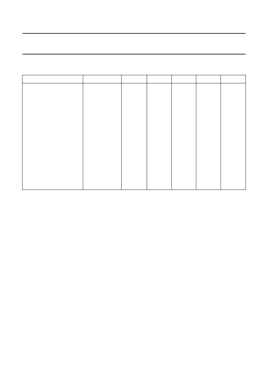
PARAMETER
CONDITIONS
SYMBOL
MIN.
TYP.
MAX.
UNIT
Supply voltage range
V
P
3
6
18
V
Total quiescent current
R
L
=
∞
I
tot
−
9
16
mA
Output power
R
L
= 8
Ω;
V
P
= 6 V
P
O
−
1.2
−
W
Internal voltage gain
G
v
38
39
40
dB
Total harmonic distortion
P
O
= 0.1 W
THD
−
0.2
1.0
%
February 1994
3
Philips Semiconductors
Product specification
2 x 1 W portable/mains-fed stereo
power amplifier
TDA7053
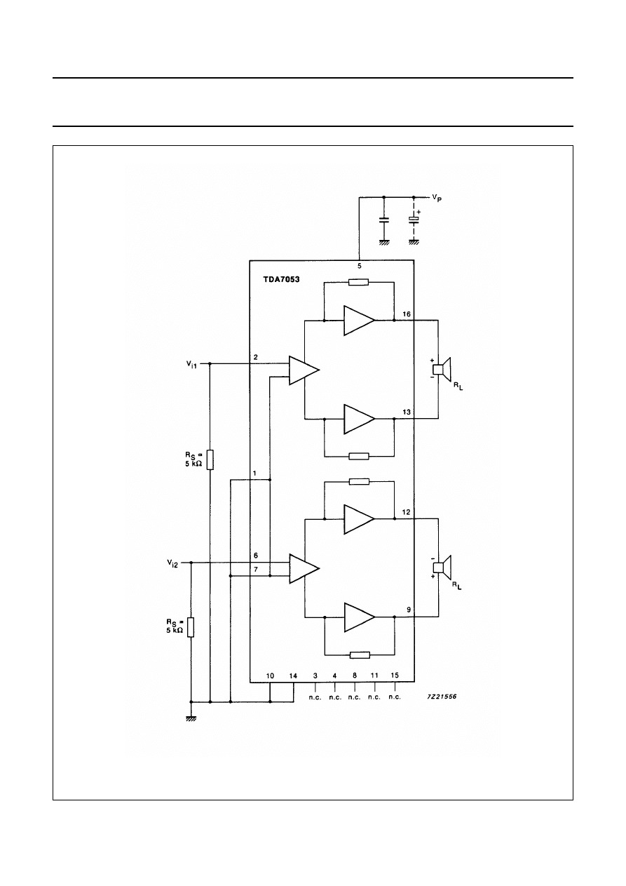
Fig.1 Block diagram.

February 1994
4
Philips Semiconductors
Product specification
2 x 1 W portable/mains-fed stereo
power amplifier
TDA7053
PINNING
Note
The information contained within the parentheses refer to the polarity of the loudspeaker terminal to which the output
must be connected.
FUNCTIONAL DESCRIPTION
The TDA7053 is a stereo output amplifier, with an internal gain of 39 dB, which is primarily for use in portable audio
applications but may also be used in mains-fed applications. The current trends in portable audio application design is
to reduce the number of batteries which results in a reduction of output power when using conventional output stages.
The TDA7053 overcomes this problem by using the Bridge-Tied-Load (BTL) principle and is capable of delivering 1.2 W
into an 8
Ω
load (V
P
= 6 V). The load can be short-circuited under all input conditions.
1.
SGND1
signal ground 1
9. OUT2A
output 2 (positive)
2.
IN1
input 1
10. GND2
power ground 2
3.
n.c.
not connected
11.
n.c.
not connected
4.
n.c.
not connected
12. OUT2B
output 2 (negative)
5.
V
P
supply voltage
13. OUT1B
output 1 (negative)
6.
IN2
input 2
14. GND1
power ground 1
7.
SGND2
signal ground 2
15. n.c.
not connected
8.
n.c.
not connected
16. OUT1A
output 1 (positive)
February 1994
5
Philips Semiconductors
Product specification
2 x 1 W portable/mains-fed stereo
power amplifier
TDA7053
RATINGS
Limiting values in accordance with the Absolute Maximum System (IEC 134)
THERMAL RESISTANCE
Power dissipation
Assuming: V
P
= 6 V and R
L
= 8
Ω
:
The maximum sinewave dissipation is 1.8 W, therefore T
amb(max.)
= 150
−
(50 x 1.8) = 60
°
C.
PARAMETER
CONDITIONS
SYMBOL
MIN.
MAX.
UNIT
Supply voltage
V
P
−
18
V
Non-repetitive peak output current
I
OSM
−
1.5
A
Total power dissipation
P
tot
see Fig.2
Crystal temperature
T
c
−
+
150
°
C
Storage temperature range
T
stg
−
55
+
150
°
C
From junction to ambient
R
th j-a
50
K/W
Fig.2 Power derating curve.
February 1994
6
Philips Semiconductors
Product specification
2 x 1 W portable/mains-fed stereo
power amplifier
TDA7053
CHARACTERISTICS
V
P
= 6 V; R
L
= 8
Ω
; T
amb
= 25
°
C; unless otherwise specified; measured from test circuit, Fig.7.
Notes to the characteristics
1. With a practical load the total quiescent current depends on the offset voltage.
2. Ripple rejection measured at the output with R
S
= 0
Ω
and f = 100 Hz to 10 kHz. The ripple voltage (200 mV) is applied
to the positive supply rail.
3. R
S
= 5 k
Ω
.
4. The noise output voltage (RMS value) is measured with R
S
= 5 k
Ω
, unweighted and a bandwidth of 60 Hz to 15 kHz.
5. The noise output voltage (RMS value) is measured with R
S
= 0
Ω
and f = 500 kHz with 5 kHz bandwidth. If R
L
= 8
Ω
and L
L
= 200
µ
H the noise output current is only 100 nA.
PARAMETER
CONDITIONS
SYMBOL
MIN.
TYP.
MAX.
UNIT
Supply voltage range
V
P
3
6
18
V
Total quiescent current
R
L
=
∞
; note 1
I
tot
−
9
16
mA
Input bias current
I
bias
−
100
300
nA
Supply voltage ripple rejection note 2
SVRR
40
50
−
dB
Input impedance
Z
I
−
100
−
k
Ω
DC output offset voltage
note 3
∆
V
13-16
−
−
100
mV
∆
V
12-9
−
−
100
mV
Noise output voltage
(RMS value)
note 4
V
no(rms)
−
150
300
µ
V
note 5
V
no(rms)
−
60
−
µ
V
Output power
THD = 10%
P
O
−
1.2
−
W
Total harmonic distortion
P
O
= 0.1 W
THD
−
0.2
1.0
%
Internal voltage gain
G
v
38
39
40
dB
Channel balance
∆
G
v
−
−
1
dB
Channel separation
note 3
α
40
−
−
dB
Frequency response
f
−
0.02 to 20
−
kHz
February 1994
7
Philips Semiconductors
Product specification
2 x 1 W portable/mains-fed stereo
power amplifier
TDA7053
APPLICATION INFORMATION
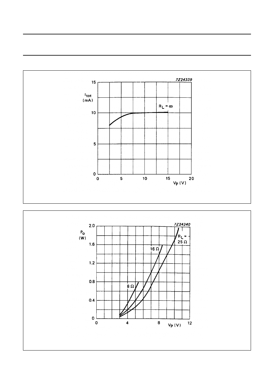
Fig.3 Quiescent current as a function of voltage supply (V
P
); T
amb
= 60
°
C.
Fig.4 Output power as a function of voltage supply (V
P
); THD = 10%; f = 1 kHz; T
amb
= 60
°
C.
February 1994
8
Philips Semiconductors
Product specification
2 x 1 W portable/mains-fed stereo
power amplifier
TDA7053
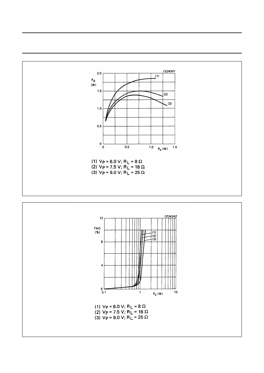
Fig.5 Power dissipation as a function of output power; f = 1 kHz; T
amb
= 60
°
C.
Fig.6 Total harmonic distortion as a function of output power; f = 1 kHz; T
amb
= 60
°
C.
February 1994
9
Philips Semiconductors
Product specification
2 x 1 W portable/mains-fed stereo
power amplifier
TDA7053
Fig.7 Test and application circuit diagram.
February 1994
10
Philips Semiconductors
Product specification
2 x 1 W portable/mains-fed stereo
power amplifier
TDA7053
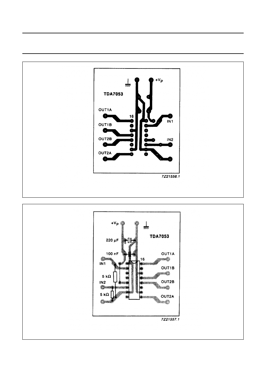
Fig.8 Printed-circuit board, track side.
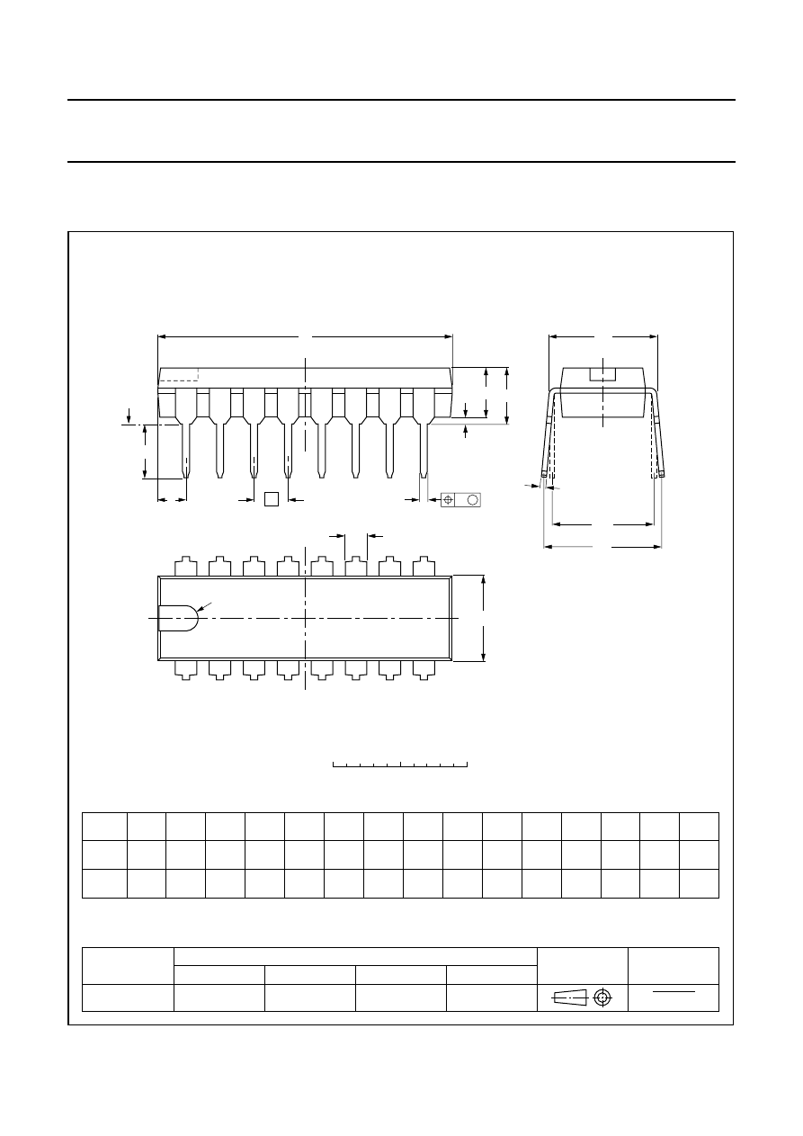
Fig.9 Printed-circuit board, component side.
February 1994
11
Philips Semiconductors
Product specification
2 x 1 W portable/mains-fed stereo
power amplifier
TDA7053
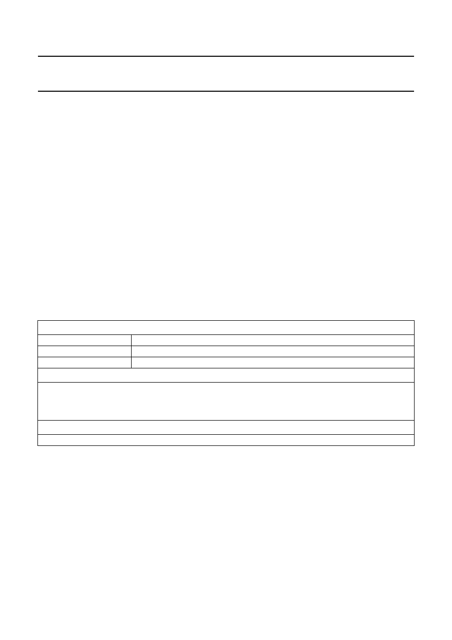
PACKAGE OUTLINE
UNIT
A
max.
1
2
b
1
c
E
e
M
H
L
REFERENCES
OUTLINE
VERSION
EUROPEAN
PROJECTION
ISSUE DATE
IEC
JEDEC
EIAJ
mm
inches
DIMENSIONS (inch dimensions are derived from the original mm dimensions)
SOT38-1
92-10-02
95-01-19
A
min.
A
max.
b
max.
w
M
E
e
1
1.40
1.14
0.055
0.045
0.53
0.38
0.32
0.23
21.8
21.4
0.86
0.84
6.48
6.20
0.26
0.24
3.9
3.4
0.15
0.13
0.254
2.54
7.62
0.30
8.25
7.80
0.32
0.31
9.5
8.3
0.37
0.33
2.2
0.087
4.7
0.51
3.7
0.15
0.021
0.015
0.013
0.009
0.01
0.10
0.020
0.19
050G09
MO-001AE
M
H
c
(e )
1
M
E
A
L
seating plane
A
1
w
M
b
1
e
D
A
2
Z
16
1
9
8
b
E
pin 1 index
0
5
10 mm
scale
Note
1. Plastic or metal protrusions of 0.25 mm maximum per side are not included.
(1)
(1)
D
(1)
Z
DIP16: plastic dual in-line package; 16 leads (300 mil); long body
SOT38-1
February 1994
12
Philips Semiconductors
Product specification
2 x 1 W portable/mains-fed stereo
power amplifier
TDA7053
SOLDERING
Introduction
There is no soldering method that is ideal for all IC
packages. Wave soldering is often preferred when
through-hole and surface mounted components are mixed
on one printed-circuit board. However, wave soldering is
not always suitable for surface mounted ICs, or for
printed-circuits with high population densities. In these
situations reflow soldering is often used.
This text gives a very brief insight to a complex technology.
A more in-depth account of soldering ICs can be found in
our
“IC Package Databook” (order code 9398 652 90011).
Soldering by dipping or by wave
The maximum permissible temperature of the solder is
260
°
C; solder at this temperature must not be in contact
with the joint for more than 5 seconds. The total contact
time of successive solder waves must not exceed
5 seconds.
The device may be mounted up to the seating plane, but
the temperature of the plastic body must not exceed the
specified maximum storage temperature (T
stg max
). If the
printed-circuit board has been pre-heated, forced cooling
may be necessary immediately after soldering to keep the
temperature within the permissible limit.
Repairing soldered joints
Apply a low voltage soldering iron (less than 24 V) to the
lead(s) of the package, below the seating plane or not
more than 2 mm above it. If the temperature of the
soldering iron bit is less than 300
°
C it may remain in
contact for up to 10 seconds. If the bit temperature is
between 300 and 400
°
C, contact may be up to 5 seconds.
DEFINITIONS
LIFE SUPPORT APPLICATIONS
These products are not designed for use in life support appliances, devices, or systems where malfunction of these
products can reasonably be expected to result in personal injury. Philips customers using or selling these products for
use in such applications do so at their own risk and agree to fully indemnify Philips for any damages resulting from such
improper use or sale.
Data sheet status
Objective specification
This data sheet contains target or goal specifications for product development.
Preliminary specification
This data sheet contains preliminary data; supplementary data may be published later.
Product specification
This data sheet contains final product specifications.
Limiting values
Limiting values given are in accordance with the Absolute Maximum Rating System (IEC 134). Stress above one or
more of the limiting values may cause permanent damage to the device. These are stress ratings only and operation
of the device at these or at any other conditions above those given in the Characteristics sections of the specification
is not implied. Exposure to limiting values for extended periods may affect device reliability.
Application information
Where application information is given, it is advisory and does not form part of the specification.
Wyszukiwarka
Podobne podstrony:
TDA7052A AT Philips elenota pl
TDA8920 Philips elenota pl
TDA8580 Philips elenota pl
TDA1517 Philips elenota pl
TDA8942P Philips elenota pl
TDA1563Q Philips elenota pl
TDA1520 Philips elenota pl
TDA8569Q Philips elenota pl
TDA8574 Philips elenota pl
TDA8924 Philips elenota pl
TDA8922 Philips elenota pl
TDA8510J Philips elenota pl (1)
TDA8552T Philips elenota pl
TDA8567Q Philips elenota pl
TDA8943SF Philips elenota pl
TDA8576T Philips elenota pl
TDA8926 Philips elenota pl
TDA8947J Philips elenota pl
więcej podobnych podstron