DATA SHEET
Product specification
File under Integrated circuits, IC01
July 1994
INTEGRATED CIRCUITS
TDA7052A/AT
1 W BTL mono audio amplifier with
DC volume control
July 1994
2
Philips Semiconductors
Product specification
1 W BTL mono audio amplifier with DC
volume control
TDA7052A/AT
FEATURES
•
DC volume control
•
Few external components
•
Mute mode
•
Thermal protection
•
Short-circuit proof
•
No switch-on and off clicks
•
Good overall stability
•
Low power consumption
•
Low HF radiation
•
ESD protected on all pins
GENERAL DESCRIPTION
The TDA7052A/AT are mono BTL output amplifiers with
DC volume control. They are designed for use in TV and
monitors, but also suitable for battery-fed portable
recorders and radios.
Missing Current Limiter (MCL)
A MCL protection circuit is built-in. The MCL circuit is
activated when the difference in current between the
output terminal of each amplifier exceeds 100 mA (typical
300 mA). This level of 100 mA allows for headphone
applications (single-ended).
QUICK REFERENCE DATA
ORDERING INFORMATION
Notes
1. SOT97-1; 1996 September 10.
2. SOT96-1; 1996 September 10.
SYMBOL
PARAMETERS
CONDITIONS
MIN.
TYP.
MAX.
UNIT
V
P
positive supply voltage range
4.5
−
18
V
P
O
output power
TDA7052A
R
L
= 8
Ω
; V
P
= 6 V
1.0
1.1
−
W
TDA7052AT
R
L
= 16
Ω
; V
P
= 6 V
0.5
0.55
−
W
G
v
maximum total voltage gain
34.5
35.5
36.5
dB
φ
gain control range
75
80
−
dB
I
P
total quiescent current
V
P
= 6 V; R
L
=
∞
−
7
12
mA
THD
total harmonic distortion
TDA7052A
P
O
= 0.5 W
−
0.3
1
%
TDA7052AT
P
O
= 0.25 W
−
0.3
1
%
EXTENDED TYPE
NUMBER
PACKAGE
PINS
PIN POSITION
MATERIAL
CODE
TDA7052A
8
DIL
plastic
SOT97
(1)
TDA7052AT
8
mini-pack
plastic
SOT96A
(2)
July 1994
3
Philips Semiconductors
Product specification
1 W BTL mono audio amplifier with DC
volume control
TDA7052A/AT
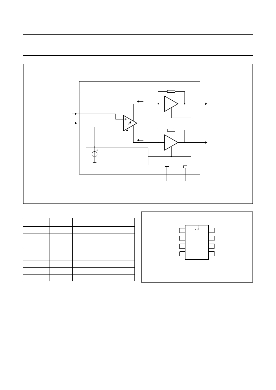
handbook, full pagewidth
positive input
6
MCD385 - 1
1
2
TDA7052A
TDA7052AT
VP
4
5
I + i
8
I – i
TEMPERATURE
PROTECTION
3
signal
ground
DC volume
control
7
n.c.
positive output
negative output
power
ground
V
ref
STABILIZER
Fig.1 Block diagram.
PINNING
SYMBOL
PIN
DESCRIPTION
V
P
1
positive supply voltage
IN+
2
positive input
GND1
3
signal ground
VC
4
DC volume control
OUT+
5
positive output
GND2
6
power ground
n.c
7
not connected
OUT
−
8
negative output
handbook, halfpage
1
2
3
4
8
7
6
5
MCD384
VP
OUT –
GND2
OUT +
GND1
IN +
VC
n.c.
TDA7052A
TDA7052AT
Fig.2 Pin configuration.
July 1994
4
Philips Semiconductors
Product specification
1 W BTL mono audio amplifier with DC
volume control
TDA7052A/AT
FUNCTIONAL DESCRIPTION
The TDA7052A/AT are mono BTL output amplifiers with
DC volume control, designed for use in TV and monitors
but also suitable for battery fed portable recorders and
radios.
In conventional DC volume circuits the control or input
stage is AC coupled to the output stage via external
capacitors to keep the offset voltage low.
In the TDA7052A/AT the DC volume control stage is
integrated into the input stage so that no coupling
capacitors are required and yet a low offset voltage is
maintained. At the same time the minimum supply remains
low.
The BTL principle offers the following advantages:
•
Lower peak value of the supply current
•
The frequency of the ripple on the supply voltage is twice
the signal frequency.
Thus a reduced power supply with smaller capacitors can
be used which results in cost savings.
For portable applications there is a trend to decrease the
supply voltage, resulting in a reduction of output power at
conventional output stages. Using the BTL principle
increases the output power.
The maximum gain of the amplifier is fixed at 35.5 dB. The
DC volume control stage has a logarithmic control
characteristic.
The total gain can be controlled from 35.5 dB to
−
44 dB. If
the DC volume control voltage is below 0.3 V, the device
switches to the mute mode.
The amplifier is short-circuit proof to ground, V
P
and
across the load. Also a thermal protection circuit is
implemented. If the crystal temperature rises above
+150
°
C the gain will be reduced, so the output power is
reduced.
Special attention is given to switch on and off clicks, low
HF radiation and a good overall stability.
LIMITING VALUES
In accordance with the Absolute Maximum System (IEC 134)
SYMBOL
PARAMETER
CONDITIONS
MIN.
MAX.
UNIT
V
P
supply voltage range
−
18
V
I
ORM
repetitive peak output current
−
1.25
A
I
OSM
non-repetitive peak output current
−
1.5
A
P
tot
total power dissipation
T
amb
≤
25%
TDA7052A
−
1.25
W
TDA7052AT
−
0.8
W
T
amb
operating ambient temperature range
−
40
+85
°
C
T
stg
storage temperature range
−
55
+150
°
C
T
vj
virtual junction temperature
−
+150
°
C
T
sc
short-circuit time
−
1
hr
V
2
input voltage pin 2
−
8
V
V
4
input voltage pin 4
−
8
V

July 1994
5
Philips Semiconductors
Product specification
1 W BTL mono audio amplifier with DC
volume control
TDA7052A/AT
THERMAL RESISTANCE
Notes to the thermal resistance
TDA7052A: V
P
= 6 V; R
L
= 8
Ω
. The maximum sine-wave dissipation is 0.9 W.
Therefore T
amb(max)
= 150
−
100
×
0.9 = 60
°
C.
TDA7052AT: V
P
= 6 V; R
L
= 16
Ω
. The maximum sine-wave dissipation is 0.46 W.
Therefore T
amb(max)
= 150
−
155
×
0.46 = 78
°
C.
SYMBOL
PARAMETER
THERMAL RESISTANCE
R
th j-a
from junction to ambient in free air
TDA7052A
100 K/W
TDA7052AT
155 K/W
July 1994
6
Philips Semiconductors
Product specification
1 W BTL mono audio amplifier with DC
volume control
TDA7052A/AT
CHARACTERISTICS
V
P
= 6 V; T
amb
= 25
°
C; f = 1 kHz; TDA7052A: R
L
= 8
Ω
; TDA7052AT: R
L
= 16
Ω
; unless otherwise specified (see Fig.6).
Notes to the characteristics
1. With a load connected to the outputs the quiescent current will increase, the maximum value of this increase being
equal to the DC output offset voltage dividend by R
L
.
2. The noise output voltage (RMS value) at f = 500 kHz is measured with R
S
= 0
Ω
and bandwidth = 5 kHz.
3. The ripple rejection is measured with R
S
= 0
Ω
and f = 100 Hz to 10 kHz. The ripple voltage of 200 mV, (RMS value)
is applied to the positive supply rail.
4. The noise output voltage (RMS value) is measured with R
S
= 5 k
Ω
unweighted.
SYMBOL
PARAMETER
CONDITIONS
MIN.
TYP.
MAX.
UNIT
V
P
positive supply voltage range
4.5
−
18
V
I
P
total quiescent current
V
P
= 6 V; R
L
=
∞
note 1
−
7
12
mA
Maximum gain; V
4
= 1.4 V
P
O
output power
THD = 10%
TDA7052A
1.0
1.1
−
W
TDA7052AT
0.5
0.55
−
W
THD
total harmonic distortion
TDA7052A
P
O
= 0.5 W
−
0.3
1
%
TDA7052AT
P
O
= 0.25 W
−
0.3
1
%
G
v
voltage gain
34.5
35.5
36.5
dB
V
I
input signal handling
V
4
= 0.8 V; THD
<
1%
0.5
0.65
−
V
V
no(rms)
noise output voltage (RMS value)
f = 500 kHz; note 2
−
210
−
µ
V
B
bandwidth
−
1 dB
−
20 Hz to
300 kHz
−
SVRR
supply voltage ripple rejection
note 3
38
46
−
dB
|
V
off
|
DC output offset voltage
−
0
150
mV
Z
I
input impedance (pin 2)
15
20
25
k
Ω
Minimum gain; V
4
= 0.5 V
G
v
voltage gain
−
−
44
−
dB
V
no(rms)
noise output voltage (RMS value)
note 4
−
20
30
µ
V
Mute position
V
O
output voltage in mute position
V
4
≤
0.3 V; V
I
= 600 mV
−
−
30
µ
V
DC volume control
φ
gain control range
75
80
−
dB
I
4
control current
V
4
= 0.4 V
60
70
80
µ
A
July 1994
7
Philips Semiconductors
Product specification
1 W BTL mono audio amplifier with DC
volume control
TDA7052A/AT
handbook, halfpage
MCD388
40
– 80
20
– 20
– 40
0
0
1.2
2.0
0.4
1.6
0.8
V
(V)
4
gain
(dB)
– 60
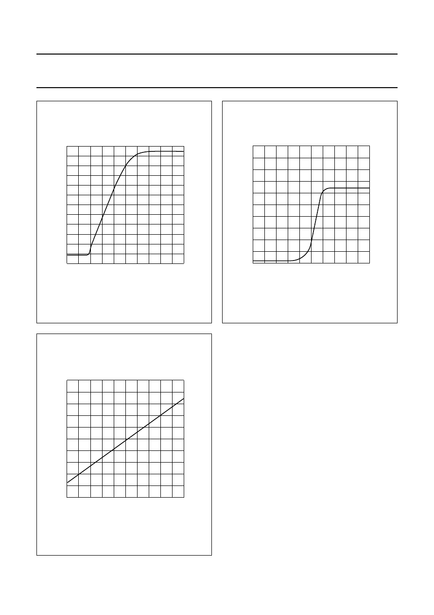
Fig.3 Gain control as a function of DC volume control.
handbook, halfpage
1000
0
800
400
200
600
0
1.2
2.0
MCD389 - 1
0.4
1.6
0.8
V (V)
4
V
noise
(
µ
V)
Fig.4
Noise output voltage as a function of DC
volume control.
handbook, halfpage
0
1.2
2.0
100
– 20
MCD390 - 1
60
20
– 60
– 100
0.4
1.6
0.8
V (V)
4
I4
(
µ
A)
Fig.5
Control current as a function of DC volume
control.
July 1994
8
Philips Semiconductors
Product specification
1 W BTL mono audio amplifier with DC
volume control
TDA7052A/AT
APPLICATION INFORMATION
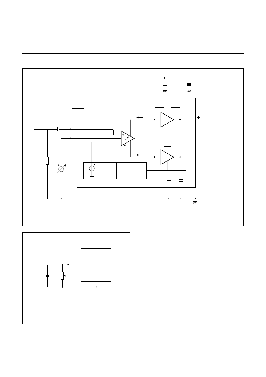
handbook, full pagewidth
positive
input
5 k
Ω
0.47
µ
F
R
S
6
MCD386 - 1
100 nF
220
µ
F
1
2
R = 8
Ω
L
TDA7052A
TDA7052AT
R = 16
Ω
L
V = 6 V
P
(1)
4
5
I + i
8
I – i
V
ref
STABILIZER
TEMPERATURE
PROTECTION
3
ground
(TDA7052A)
(TDA7052A/AT)
DC
volume
control
7
n.c.
Fig.6 Test and application diagram.
This capacitor can be omitted if the 220
µ
F electrolytic capacitor is connected close to pin 1.
handbook, halfpage
MCD387
4
volume
control
1 M
Ω
1
µ
F
Fig.7
Application with potentiometer as volume
control; maximum gain = 30 dB.
July 1994
9
Philips Semiconductors
Product specification
1 W BTL mono audio amplifier with DC
volume control
TDA7052A/AT
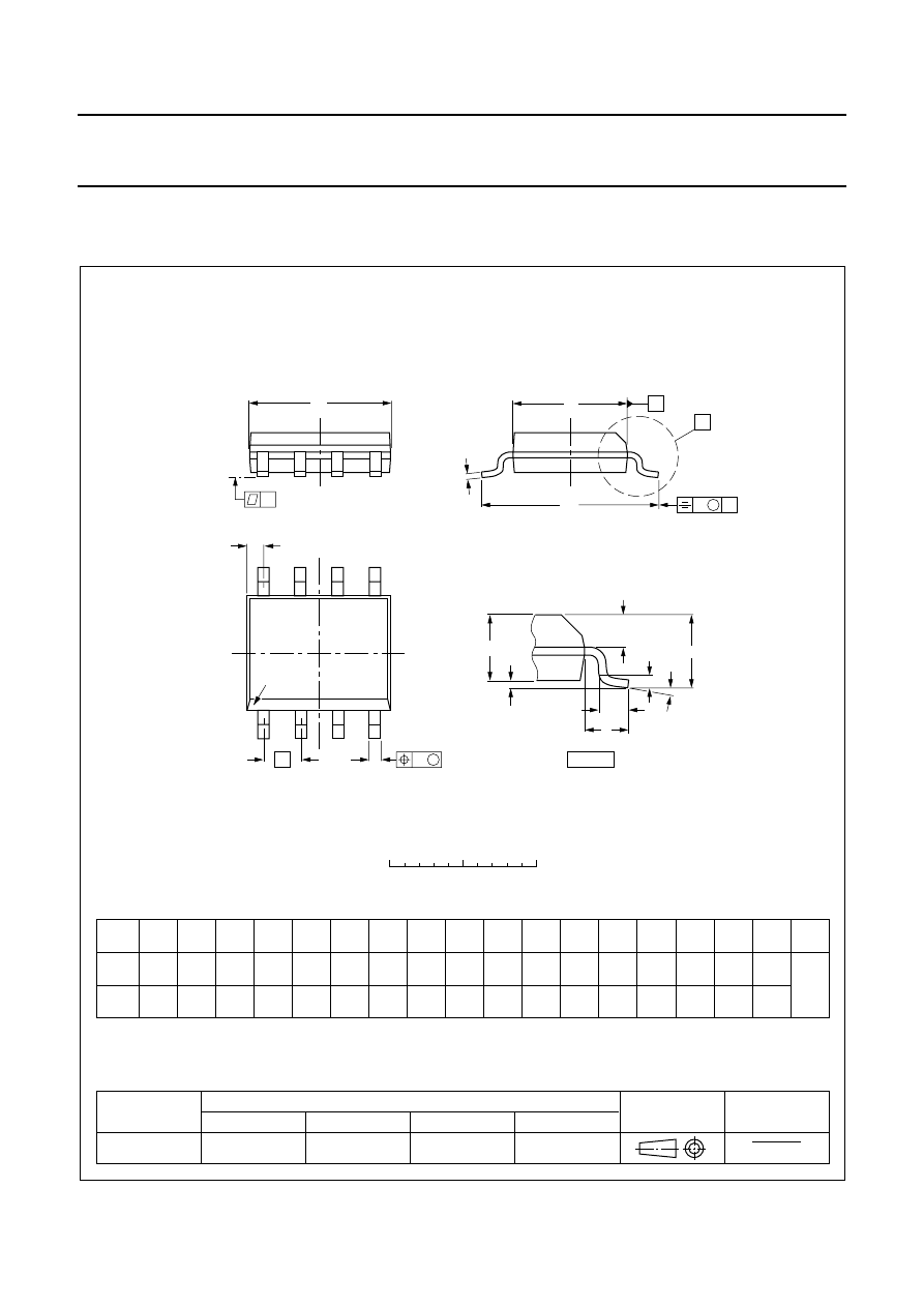
PACKAGE OUTLINES
REFERENCES
OUTLINE
VERSION
EUROPEAN
PROJECTION
ISSUE DATE
IEC
JEDEC
EIAJ
SOT97-1
92-11-17
95-02-04
UNIT
A
max.
1
2
b
1
(1)
(1)
(1)
b
2
c
D
E
e
M
Z
H
L
mm
DIMENSIONS (inch dimensions are derived from the original mm dimensions)
A
min.
A
max.
b
max.
w
M
E
e
1
1.73
1.14
0.53
0.38
0.36
0.23
9.8
9.2
6.48
6.20
3.60
3.05
0.254
2.54
7.62
8.25
7.80
10.0
8.3
1.15
4.2
0.51
3.2
inches
0.068
0.045
0.021
0.015
0.014
0.009
1.07
0.89
0.042
0.035
0.39
0.36
0.26
0.24
0.14
0.12
0.01
0.10
0.30
0.32
0.31
0.39
0.33
0.045
0.17
0.020
0.13
b
2
050G01
MO-001AN
M
H
c
(e )
1
M
E
A
L
seating plane
A
1
w
M
b
1
e
D
A
2
Z
8
1
5
4
b
E
0
5
10 mm
scale
Note
1. Plastic or metal protrusions of 0.25 mm maximum per side are not included.
pin 1 index
DIP8: plastic dual in-line package; 8 leads (300 mil)
SOT97-1
July 1994
10
Philips Semiconductors
Product specification
1 W BTL mono audio amplifier with DC
volume control
TDA7052A/AT
UNIT
A
max.
A
1
A
2
A
3
b
p
c
D
(1)
E
(2)
(1)
e
H
E
L
L
p
Q
Z
y
w
v
θ
REFERENCES
OUTLINE
VERSION
EUROPEAN
PROJECTION
ISSUE DATE
IEC
JEDEC
EIAJ
mm
inches
1.75
0.25
0.10
1.45
1.25
0.25
0.49
0.36
0.25
0.19
5.0
4.8
4.0
3.8
1.27
6.2
5.8
1.05
0.7
0.6
0.7
0.3
8
0
o
o
0.25
0.1
0.25
DIMENSIONS (inch dimensions are derived from the original mm dimensions)
Notes
1. Plastic or metal protrusions of 0.15 mm maximum per side are not included.
2. Plastic or metal protrusions of 0.25 mm maximum per side are not included.
1.0
0.4
SOT96-1
X
w
M
θ
A
A
1
A
2
b
p
D
H
E
L
p
Q
detail X
E
Z
e
c
L
v
M
A
(A )
3
A
4
5
pin 1 index
1
8
y
076E03S
MS-012AA
0.069
0.010
0.004
0.057
0.049
0.01
0.019
0.014
0.0100
0.0075
0.20
0.19
0.16
0.15
0.050
0.244
0.228
0.028
0.024
0.028
0.012
0.01
0.01
0.041
0.004
0.039
0.016
0
2.5
5 mm
scale
SO8: plastic small outline package; 8 leads; body width 3.9 mm
SOT96-1
95-02-04
97-05-22

July 1994
11
Philips Semiconductors
Product specification
1 W BTL mono audio amplifier with DC
volume control
TDA7052A/AT
SOLDERING
Introduction
There is no soldering method that is ideal for all IC
packages. Wave soldering is often preferred when
through-hole and surface mounted components are mixed
on one printed-circuit board. However, wave soldering is
not always suitable for surface mounted ICs, or for
printed-circuits with high population densities. In these
situations reflow soldering is often used.
This text gives a very brief insight to a complex technology.
A more in-depth account of soldering ICs can be found in
our
“IC Package Databook” (order code 9398 652 90011).
DIP
S
OLDERING BY DIPPING OR BY WAVE
The maximum permissible temperature of the solder is
260
°
C; solder at this temperature must not be in contact
with the joint for more than 5 seconds. The total contact
time of successive solder waves must not exceed
5 seconds.
The device may be mounted up to the seating plane, but
the temperature of the plastic body must not exceed the
specified maximum storage temperature (T
stg max
). If the
printed-circuit board has been pre-heated, forced cooling
may be necessary immediately after soldering to keep the
temperature within the permissible limit.
R
EPAIRING SOLDERED JOINTS
Apply a low voltage soldering iron (less than 24 V) to the
lead(s) of the package, below the seating plane or not
more than 2 mm above it. If the temperature of the
soldering iron bit is less than 300
°
C it may remain in
contact for up to 10 seconds. If the bit temperature is
between 300 and 400
°
C, contact may be up to 5 seconds.
SO
R
EFLOW SOLDERING
Reflow soldering techniques are suitable for all SO
packages.
Reflow soldering requires solder paste (a suspension of
fine solder particles, flux and binding agent) to be applied
to the printed-circuit board by screen printing, stencilling or
pressure-syringe dispensing before package placement.
Several techniques exist for reflowing; for example,
thermal conduction by heated belt. Dwell times vary
between 50 and 300 seconds depending on heating
method. Typical reflow temperatures range from
215 to 250
°
C.
Preheating is necessary to dry the paste and evaporate
the binding agent. Preheating duration: 45 minutes at
45
°
C.
W
AVE SOLDERING
Wave soldering techniques can be used for all SO
packages if the following conditions are observed:
•
A double-wave (a turbulent wave with high upward
pressure followed by a smooth laminar wave) soldering
technique should be used.
•
The longitudinal axis of the package footprint must be
parallel to the solder flow.
•
The package footprint must incorporate solder thieves at
the downstream end.
During placement and before soldering, the package must
be fixed with a droplet of adhesive. The adhesive can be
applied by screen printing, pin transfer or syringe
dispensing. The package can be soldered after the
adhesive is cured.
Maximum permissible solder temperature is 260
°
C, and
maximum duration of package immersion in solder is
10 seconds, if cooled to less than 150
°
C within
6 seconds. Typical dwell time is 4 seconds at 250
°
C.
A mildly-activated flux will eliminate the need for removal
of corrosive residues in most applications.
R
EPAIRING SOLDERED JOINTS
Fix the component by first soldering two diagonally-
opposite end leads. Use only a low voltage soldering iron
(less than 24 V) applied to the flat part of the lead. Contact
time must be limited to 10 seconds at up to 300
°
C. When
using a dedicated tool, all other leads can be soldered in
one operation within 2 to 5 seconds between
270 and 320
°
C.

July 1994
12
Philips Semiconductors
Product specification
1 W BTL mono audio amplifier with DC
volume control
TDA7052A/AT
DEFINITIONS
LIFE SUPPORT APPLICATIONS
These products are not designed for use in life support appliances, devices, or systems where malfunction of these
products can reasonably be expected to result in personal injury. Philips customers using or selling these products for
use in such applications do so at their own risk and agree to fully indemnify Philips for any damages resulting from such
improper use or sale.
Data sheet status
Objective specification
This data sheet contains target or goal specifications for product development.
Preliminary specification
This data sheet contains preliminary data; supplementary data may be published later.
Product specification
This data sheet contains final product specifications.
Limiting values
Limiting values given are in accordance with the Absolute Maximum Rating System (IEC 134). Stress above one or
more of the limiting values may cause permanent damage to the device. These are stress ratings only and operation
of the device at these or at any other conditions above those given in the Characteristics sections of the specification
is not implied. Exposure to limiting values for extended periods may affect device reliability.
Application information
Where application information is given, it is advisory and does not form part of the specification.
Document Outline
- FEATURES
- GENERAL DESCRIPTION
- QUICK REFERENCE DATA
- ORDERING INFORMATION
- PINNING
- FUNCTIONAL DESCRIPTION
- LIMITING VALUES
- THERMAL RESISTANCE
- CHARACTERISTICS
- APPLICATION INFORMATION
- PACKAGE OUTLINES
- SOLDERING
- DEFINITIONS
- LIFE SUPPORT APPLICATIONS
Wyszukiwarka
Podobne podstrony:
TDA7072A AT Philips elenota pl
TDA7053 Philips elenota pl
TDA8920 Philips elenota pl
TDA8580 Philips elenota pl
TDA1517 Philips elenota pl
TDA8942P Philips elenota pl
TDA1563Q Philips elenota pl
TDA1520 Philips elenota pl
TDA8569Q Philips elenota pl
TDA8574 Philips elenota pl
TDA8924 Philips elenota pl
TDA8922 Philips elenota pl
TDA8510J Philips elenota pl (1)
TDA8552T Philips elenota pl
TDA8567Q Philips elenota pl
TDA8943SF Philips elenota pl
TDA8576T Philips elenota pl
TDA8926 Philips elenota pl
więcej podobnych podstron