PWP
RHB
NT
www.ti.com
FEATURES
APPLICATIONS
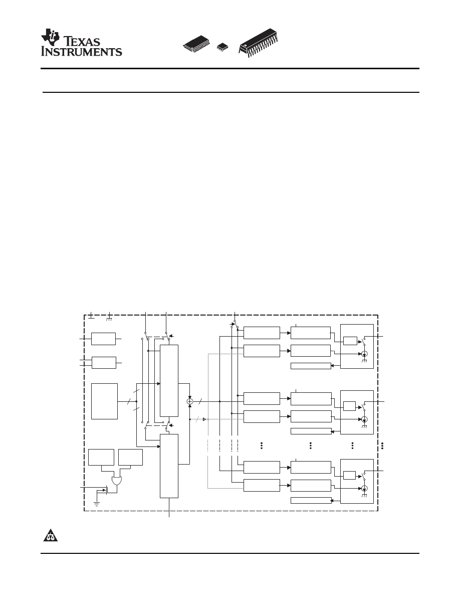
DESCRIPTION
Delay
x0
6−Bit Dot Correction
12−Bit Grayscale
PWM Control
DC Register
GS Register
Constant-Current
Driver
LED Open Detection
Temperature
Error Flag
(TEF)
Max. OUTn
Current
Delay
x1
6−Bit Dot Correction
12−Bit Grayscale
PWM Control
DC Register
GS Register
Constant-Current
Driver
LED Open Detection
Delay
x15
6−Bit Dot Correction
12−Bit Grayscale
PWM Control
DC Register
GS Register
Constant-Current
Driver
LED Open Detection
OUT0
OUT1
OUT15
SOUT
SIN
SCLK
IREF
XLAT
GSCLK
BLANK
GND
VCC
MODE
Input
Shift
Register
Input
Shift
Register
MODE
11
0
23
12
191
180
95
90
5
MODE
0
95
96
191
LED Open
Detection
(LOD)
6
11
0
192
96
0
1
0
1
0
1
GS Counter
CNT
CNT
CNT
CNT
96
96
Status
Information:
LOD,
TED,
DC DATA
192
0
191
VREF
=1.24V
XERR
SLVS589B – JULY 2005 – REVISED APRIL 2007
16-CHANNEL LED DRIVER WITH DOT CORRECTION AND GRAYSCALE PWM CONTROL
•
Monocolor, Multicolor, Full-Color LED
•
16 Channels
Displays
•
12-bit (4096 Steps) Grayscale PWM Control
•
LED Signboards
•
Dot Correction
•
Display Back-lighting
–
6 bit (64 Steps)
•
Drive Capability (Constant-Current Sink)
–
0 mA to 80 mA
The TLC5941 is a 16-channel, constant-current sink,
•
LED Power Supply Voltage up to 17 V
LED
driver.
Each
channel
has
an
individually
adjustable 4096-step grayscale PWM brightness
•
V
CC
= 3.0 V to 5.5 V
control and a 64-step constant-current sink (dot
•
Serial Data Interface
correction). The dot correction adjusts the brightness
•
Controlled In-Rush Current
variations between LED channels and other LED
drivers. Both grayscale control and dot correction are
•
30-MHz Data Transfer Rate
accessible via a serial interface. A single external
•
CMOS Level I/O
resistor sets the maximum current value of all 16
•
Error Information
channels.
–
LOD: LED Open Detection
The TLC5941 features two error information circuits.
–
TEF: Thermal Error Flag
The LED open detection (LOD) indicates a broken or
disconnected LED at an output terminal. The thermal
error
flag
(TEF)
indicates
an
overtemperature
condition.
Please be aware that an important notice concerning availability, standard warranty, and use in critical applications of Texas
Instruments semiconductor products and disclaimers thereto appears at the end of this data sheet.
PowerPAD is a trademark of Texas Instruments.
PRODUCTION DATA information is current as of publication date.
Copyright © 2005–2007, Texas Instruments Incorporated
Products conform to specifications per the terms of the Texas
Instruments standard warranty. Production processing does not
necessarily include testing of all parameters.
www.ti.com
ABSOLUTE MAXIMUM RATINGS.
SLVS589B – JULY 2005 – REVISED APRIL 2007
These devices have limited built-in ESD protection. The leads should be shorted together or the device placed in conductive foam
during storage or handling to prevent electrostatic damage to the MOS gates.
ORDERING INFORMATION
T
A
PACKAGE
(1)
PART NUMBER
–40
°
C to 85
°
C
28-pin HTSSOP PowerPAD™
TLC5941PWP
–40
°
C to 85
°
C
32-pin 5 mm x 5 mm QFN
TLC5941RHB
–40
°
C to 85
°
C
28-pin PDIP
TLC5941NT
(1)
For the most current package and ordering information, see the Package Option Addendum at the end
of this document, or see the TI Web site at
.
over operating free-air temperature range (unless otherwise noted)
(1)
UNIT
V
I
Input voltage range
(2)
VCC
–0.3 V to 6 V
I
O
Output current (dc)
90 mA
V
I
Input voltage range
V
(BLANK)
, V
(SCLK)
, V
(XLAT)
, V
(MODE)
, V
(SIN)
, V
(GSCLK)
, V
(IREF)
, V
(TEST)
–0.3 V to V
CC
+0.3 V
V
(SOUT)
, V
(XERR)
–0.3 V to V
CC
+0.3 V
V
O
Output voltage range
V
(OUT0)
to V
(OUT15)
–0.3 V to 18 V
HBM (JEDEC JESD22-A114, Human Body Model)
2 kV
ESD rating
CDM (JEDEC JESD22-C101, Charged Device Model)
500 V
T
stg
Storage temperature range
–55
°
C to 150
°
C
T
A
Operating ambient temperature range
–40
°
C to 85
°
C
HTSSOP (PWP)
(4)
31.58
°
C/W
Package thermal impedance
(3)
QFN (RHB)
(4)
35.9
°
C/W
PDIP (NT)
48
°
C/W
(1)
Stresses beyond those listed under absolute maximum ratings may cause permanent damage to the device. These are stress ratings
only, and functional operation of the device at these or any other conditions beyond those indicated under recommended operating
conditions is not implied. Exposure to absolute maximum rated conditions for extended periods may affect device reliability.
(2)
All voltage values are with respect to network ground terminal.
(3)
The package thermal impedance is calculated in accordance with JESD 51-7.
(4)
With PowerPAD soldered on PCB with 2-oz. trace of copper. See TI application report SLMA002 for further information.
2
www.ti.com
RECOMMENDED OPERATING CONDITIONS
DISSIPATION RATINGS
SLVS589B – JULY 2005 – REVISED APRIL 2007
PARAMETER
TEST CONDITIONS
MIN
NOM
MAX
UNIT
DC Characteristics
V
CC
Supply Voltage
3
5.5
V
V
O
Voltage applied to output (OUT0 - OUT15)
17
V
V
IH
High-level input voltage
0.8 V
CC
V
CC
V
V
IL
Low-level input voltage
GND
0.2 V
CC
V
I
OH
High-level output current
V
CC
= 5 V at SOUT
–1
mA
I
OL
Low-level output current
V
CC
= 5 V at SOUT, XERR
1
mA
I
OLC
Constant output current
OUT0 to OUT15
80
mA
T
A
Operating free-air temperature range
–40
85
°
C
AC Characteristics
V
CC
= 3 V to 5.5 V, T
A
= –40
°
C to 85
°
C (unless otherwise noted)
Data shift clock
f
(SCLK)
SCLK
30
MHz
frequency
Grayscale clock
f
(GSCLK)
GSCLK
30
MHz
frequency
t
wh0
/t
wl0
SCLK pulse duration
SCLK = H/L (See
16
ns
t
wh1
/t
wl1
GSCLK pulse duration
GSCLK = H/L (See
16
ns
t
wh2
XLAT pulse duration
XLAT = H (See
)
20
ns
t
wh3
BLANK pulse duration
BLANK = H (See
20
ns
t
su0
SIN - SCLK
↑
(See
5
t
su1
SCLK
↓
- XLAT
↑
(See
10
t
su2
MODE
↑↓
- SCLK
↑
(See
)
10
Setup time
ns
t
su3
MODE
↑↓
- XLAT
↑
(See
10
t
su4
BLANK
↓
- GSCLK
↑
(See
10
t
su5
XLAT
↑
- GSCLK
↑
(See
30
t
h0
SCLK
↑
- SIN (See
3
t
h1
XLAT
↓
- SCLK
↑
(See
)
10
t
h2
Hold Time
SCLK
↑
- MODE
↑↓
(See
)
10
ns
t
h3
XLAT
↓
- MODE
↑↓
(See
10
t
h4
GSCLK
↑
- BLANK
↑
(See
10
POWER RATING
POWER RATING
POWER RATING
PACKAGE
DERATING FACTOR ABOVE T
A
= 25
°
C
T
A
< 25
°
C
T
A
= 70
°
C
T
A
= 85
°
C
28-pin HTSSOP with
PowerPAD™
3958 mW
31.67 mW/
°
C
2533 mW
2058 mW
soldered
(1)
28-pin HTSSOP
without PowerPAD™
2026 mW
16.21 mW/
°
C
1296 mW
1053 mW
soldered
32-pin QFN
(1)
3482 mW
27.86 mW/
°
C
2228 mW
1811 mW
28-pin PDIP
2456 mW
19.65 mW/
°
C
1572 mW
1277 mW
(1)
The PowerPAD is soldered to the PCB with a 2-oz. copper trace. See application report
SLMA002
for further information.
3
www.ti.com
ELECTRICAL CHARACTERISTICS
SLVS589B – JULY 2005 – REVISED APRIL 2007
V
CC
= 3 V to 5.5 V, T
A
= -40
°
C to 85
°
C (unless otherwise noted)
PARAMETER
TEST CONDITIONS
MIN
TYP
MAX UNI
T
V
OH
High-level output
I
OH
= –1 mA, SOUT
V
CC
–0.5
V
voltage
V
OL
Low-level output
I
OL
= 1 mA, SOUT
0.5
V
voltage
V
I
= V
CC
or GND; BLANK, TEST, GSCLK, SCLK, SIN, XLAT pin
–1
1
I
I
Input current
V
I
= GND; MODE pin
–1
1
µ
A
V
I
= V
CC
; MODE pin
50
No data transfer, all output OFF, V
O
= 1 V, R
(IREF)
= 10 k
Ω
0.9
6
No data transfer, all output OFF, V
O
= 1 V, R
(IREF)
= 1.3 k
Ω
5.2
12
I
CC
Supply current
mA
Data transfer 30 MHz, all output ON, V
O
= 1 V, R
(IREF)
= 1.3 k
Ω
16
25
Data transfer 30 MHz, all output ON, V
O
= 1 V, R
(IREF)
= 640
Ω
30
60
I
O(LC)
Constant output current All output ON, V
O
= 1 V, R
(IREF)
= 640
Ω
54
61
69 mA
I
lkg
Leakage output current
All output OFF, V
O
= 15 V, R
(IREF)
= 640
Ω
, OUT0 to OUT15
0.1
µ
A
All output ON, V
O
= 1 V, R
(IREF)
= 640
Ω
, OUT0 to OUT15,
±
1
±
4
%
–20
°
C to 85
°
C
(1)
All output ON, V
O
= 1 V, R
(IREF)
= 640
Ω
, OUT0 to OUT15
(1)
±
1
±
8
Constant sink current
∆
I
O(LC0)
error
All output ON, V
O
= 1 V, R
(IREF)
= 480
Ω
, OUT0 to OUT15,
±
1
±
6
%
–20
°
C to 85
°
C
(1)
All output ON, V
O
= 1 V, R
(IREF)
= 480
Ω
, OUT0 to OUT15
(1)
±
1
±
8
Constant sink current
Device to device, averaged current from OUT0 to OUT15,
–2,
∆
I
O(LC1)
±
4
%
error
R
(IREF)
= 1920
Ω
(20 mA)
(2)
0.4
Constant sink current
Device to device, averaged current from OUT0 to OUT15,
–2.7,
∆
I
O(LC2)
±
4
%
error
R
(IREF)
= 480
Ω
(80 mA)
(2)
2
All output ON, V
O
= 1 V, R
(IREF)
= 640
Ω
OUT0 to OUT15,
±
1
±
4
V
CC
= 3 V to 5.5 V
(3)
%/
∆
I
O(LC3)
Line regulation
V
All output ON, V
O
= 1 V, R
(IREF)
= 480
Ω
OUT0 to OUT15,
±
1
±
6
V
CC
= 3 V to 5.5 V
(3)
All output ON, V
O
= 1 V to 3 V, R
(IREF)
= 640
Ω
, OUT0 to OUT15
(4)
±
2
±
6
%/
∆
I
O(LC4)
Load regulation
V
All output ON, V
O
= 1 V to 3 V, R
(IREF)
= 480
Ω
, OUT0 to OUT15
(4)
±
2
±
8
Thermal error flag
T
(TEF)
Junction temperature
(5)
150
170
°
C
threshold
LED open detection
V
(LED)
0.3
0.4
V
threshold
Reference voltage
V
(IREF)
R
I(REF)
= 640
Ω
1.20
1.24
1.28
V
output
(1)
The deviation of each output from the average of OUT0-15 constant current. It is calculated by
in
(2)
The deviation of average of OUT1-15 constant current from the ideal constant-current value. It is calculated by
in
The ideal current is calculated by
in
(3)
The line regulation is calculated by
in
(4)
The load regulation is calculated by
in
(5)
Not tested. Specified by design.
4
www.ti.com
100
I
I
I
(%)
15
0
_
OUTavg
15
0
_
OUTavg
OUTn
´
-
=
D
-
-
(1)
100
I
I
I
(%)
)
IDEAL
(
OUT
)
IDEAL
(
OUT
OUTavg
´
-
=
D
(2)
÷÷
ø
ö
çç
è
æ
´
=
IREF
)
IDEAL
(
OUT
R
V
24
.
1
5
.
31
I
(3)
5
.
2
100
)
V
0
.
3
V
at
I
(
)
V
0
.
3
V
at
I
(
)
V
5
.
5
V
at
I
(
)
V
/
(%
CC
OUTn
CC
OUTn
CC
OUTn
´
=
=
-
=
=
D
(4)
0
.
2
100
)
V
0
.
1
V
at
I
(
)
V
0
.
1
V
at
I
(
)
V
0
.
3
V
at
I
(
)
V
/
(%
OUTn
OUTn
OUTn
OUTn
OUTn
OUTn
´
=
=
-
=
=
D
(5)
SWITCHING CHARACTERISTICS
SLVS589B – JULY 2005 – REVISED APRIL 2007
Table 1. Test Parameter Equations
V
CC
= 3 V to 5.5 V, C
L
= 15 pF, T
A
= –40
°
C to 85
°
C (unless otherwise noted)
PARAMETER
TEST CONDITIONS
MIN
TYP
MAX
UNIT
t
r0
SOUT
16
Rise time
ns
t
r1
OUTn, V
CC
= 5 V, T
A
= 60
°
C, DCn = 3Fh
10
30
t
f0
SOUT
16
Fall time
ns
t
f1
OUTn, V
CC
= 5 V, T
A
= 60
°
C, DCn = 3Fh
10
30
t
pd0
SCLK - SOUT (see
)
30
ns
t
pd1
BLANK - OUT0 (see
)
60
ns
t
pd2
Propagation delay time
OUTn - XERR (see
)
1000
ns
t
pd3
GSCLK - OUT0 (see
60
ns
t
pd4
XLAT - I
OUT
(dot correction) (see
)
1000
ns
t
d
Output delay time
OUTn - OUT(n+1) (see
)
20
30
ns
t
outon
– T
gsclk
(see
), GSn = 01h,
10
–50
–90
ns
t
on_err
Output on-time error
GSCLK = 11 MHz
5
www.ti.com
DEVICE INFORMATION
1
2
3
4
5
6
7
8
9
10
11
12
13
14
28
27
26
25
24
23
22
21
20
19
18
17
16
15
GND
BLANK
XLAT
SCLK
SIN
MODE
OUT0
OUT1
OUT2
OUT3
OUT4
OUT5
OUT6
OUT7
VCC
IREF
TEST
GSCLK
SOUT
XERR
OUT15
OUT14
OUT13
OUT12
OUT11
OUT10
OUT9
OUT8
PWP PACKAGE
(TOP VIEW)
Thermal
PAD
THERMAL
PAD
GSCLK
24
SOUT
23
XERR
22
OUT15
21
OUT14
20
OUT13
19
OUT12
18
OUT1
1
17
OUT10
16
OUT9
15
OUT8
14
NC
13
NC
12
OUT7
11
OUT6
10
OUT5
9
OUT4
8
OUT3
7
OUT2
6
OUT1
5
OUT0
4
MODE
3
SIN
2
SCLK
1
TEST
25
IREF
26
VCC
27
NC
28
NC
29
GND
30
BLANK
31
XLAT
32
RHB PACKAGE
(TOP VIEW)
NC − No internal connection
1
2
3
4
5
6
7
8
9
10
11
12
13
14
18
17
16
15
22
21
20
19
26
25
24
23
28
27
OUT1
OUT2
OUT3
OUT4
OUT5
OUT6
OUT7
OUT8
OUT9
OUT10
OUT11
OUT12
OUT13
OUT14
GND
VCC
IREF
TEST
GSCLK
SOUT
XERR
OUT15
SCLK
XLAT
BLANK
OUT0
MODE
SIN
NT PACKAGE
(TOP VIEW)
SLVS589B – JULY 2005 – REVISED APRIL 2007
6
www.ti.com
SLVS589B – JULY 2005 – REVISED APRIL 2007
DEVICE INFORMATION (continued)
TERMINAL FUNCTION
TERMINAL
NT
PWP
RHB
I/O
DESCRIPTION
NAME
NO.
NO.
NO.
Blank all outputs. When BLANK = H, all OUTn outputs are forced
BLANK
23
2
31
I
OFF. GS counter is also reset. When BLANK = L, OUTn are controlled
by grayscale PWM control.
GND
22
1
30
G
Ground
GSCLK
18
25
24
I
Reference clock for grayscale PWM control
IREF
20
27
26
I/O
Reference current terminal
NC
-
-
12, 13, 28, 29
No connection
OUT0
28
7
4
O
Constant-current output
OUT1
1
8
5
O
Constant-current output
OUT2
2
9
6
O
Constant-current output
OUT3
3
10
7
O
Constant-current output
OUT4
4
11
8
O
Constant-current output
OUT5
5
12
9
O
Constant-current output
OUT6
6
13
10
O
Constant-current output
OUT7
7
14
11
O
Constant-current output
OUT8
8
15
14
O
Constant-current output
OUT9
9
16
15
O
Constant-current output
OUT10
10
17
16
O
Constant-current output
OUT11
11
18
17
O
Constant-current output
OUT12
12
19
18
O
Constant-current output
OUT13
13
20
19
O
Constant-current output
OUT14
14
21
20
O
Constant-current output
OUT15
15
22
21
O
Constant-current output
SCLK
25
4
1
I
Serial data shift clock
SIN
26
5
2
I
Serial data input
SOUT
17
24
23
O
Serial data output
TEST
19
26
25
I
Test pin: TEST must be connected to VCC.
VCC
21
28
27
I
Power supply voltage.
Input mode-change pin. When MODE = GND, the device is in GS
MODE
27
6
3
I
mode. When MODE = V
CC
, the device is in DC mode.
Error output. XERR is an open-drain terminal. XERR goes L when
XERR
16
23
22
O
LOD or TEF is detected.
Level triggered latch signal. When XLAT = high, the TLC5941 writes
data from the input shift register to either GS register (MODE = low) or
XLAT
24
3
32
I
DC register (MODE = high). When XLAT=low, the data in the GS or
DC registers is held constant and does not change.
7
www.ti.com
PARAMETER MEASUREMENT INFORMATION
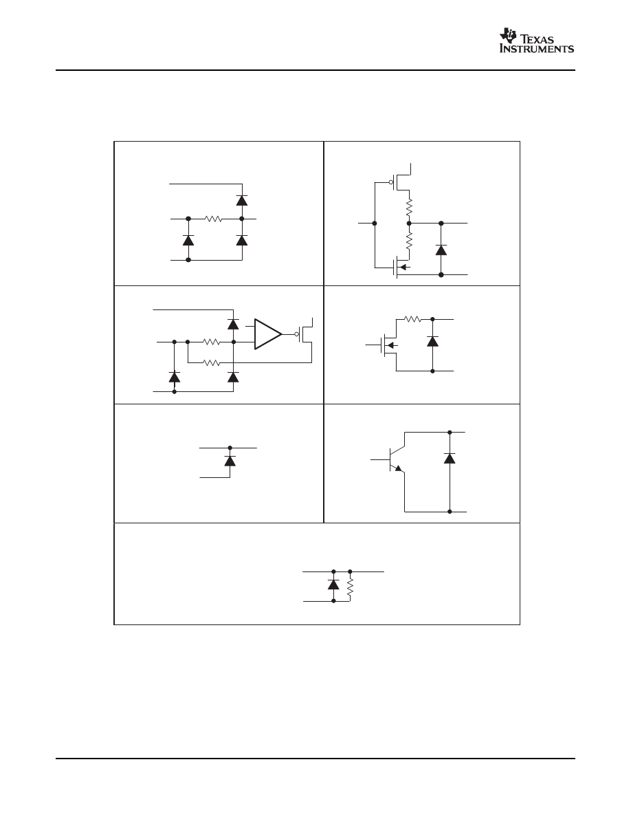
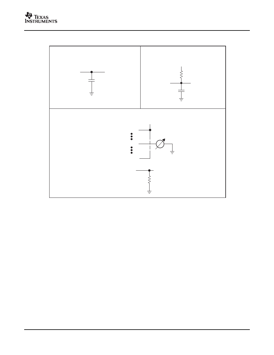
PIN EQUIVALENT INPUT AND OUTPUT SCHEMATIC DIAGRAMS
VCC
INPUT
GND
400
INPUT EQUIVALENT CIRCUIT
(BLANK, XLAT, SCLK, SIN, GSCLK, TEST)
23
23
SOUT
GND
OUTPUT EQUIVALENT CIRCUIT (SOUT)
_
+
Amp
400
100
VCC
INPUT
GND
INPUT EQUIVALENT CIRCUIT (IREF)
XERR
GND
OUTPUT EQUIVALENT CIRCUIT (XERR)
23
INPUT
GND
INPUT EQUIVALENT CIRCUIT (VCC)
OUT
GND
OUTPUT EQUIVALENT CIRCUIT (OUT)
INPUT
GND
INPUT EQUIVALENT CIRCUIT (MODE)
SLVS589B – JULY 2005 – REVISED APRIL 2007
Resistor values are equivalent resistance and not tested.
Figure 1. Input and Output Equivalent Circuits
8
www.ti.com
Test Point
C
L
= 15 pF
SOUT
V
(LED)
= 4 V
R
L
= 51
C
L
= 15 pF
OUTn
Test Point
_
+
V
CC
= 0 V ~ 7 V
V
(LED)
=
1 V
OUT0
OUTn
OUT15
Test Point
R
IREF
= 640
IREF
IOLC, IOLC3, IOLC4
t
who
, t
wIO
, t
wh1
, t
wl1
, t
su0
t
su4,
t
h4
SLVS589B – JULY 2005 – REVISED APRIL 2007
PARAMETER MEASUREMENT INFORMATION (continued)
Figure 2. Parameter Measurement Circuits
9
www.ti.com
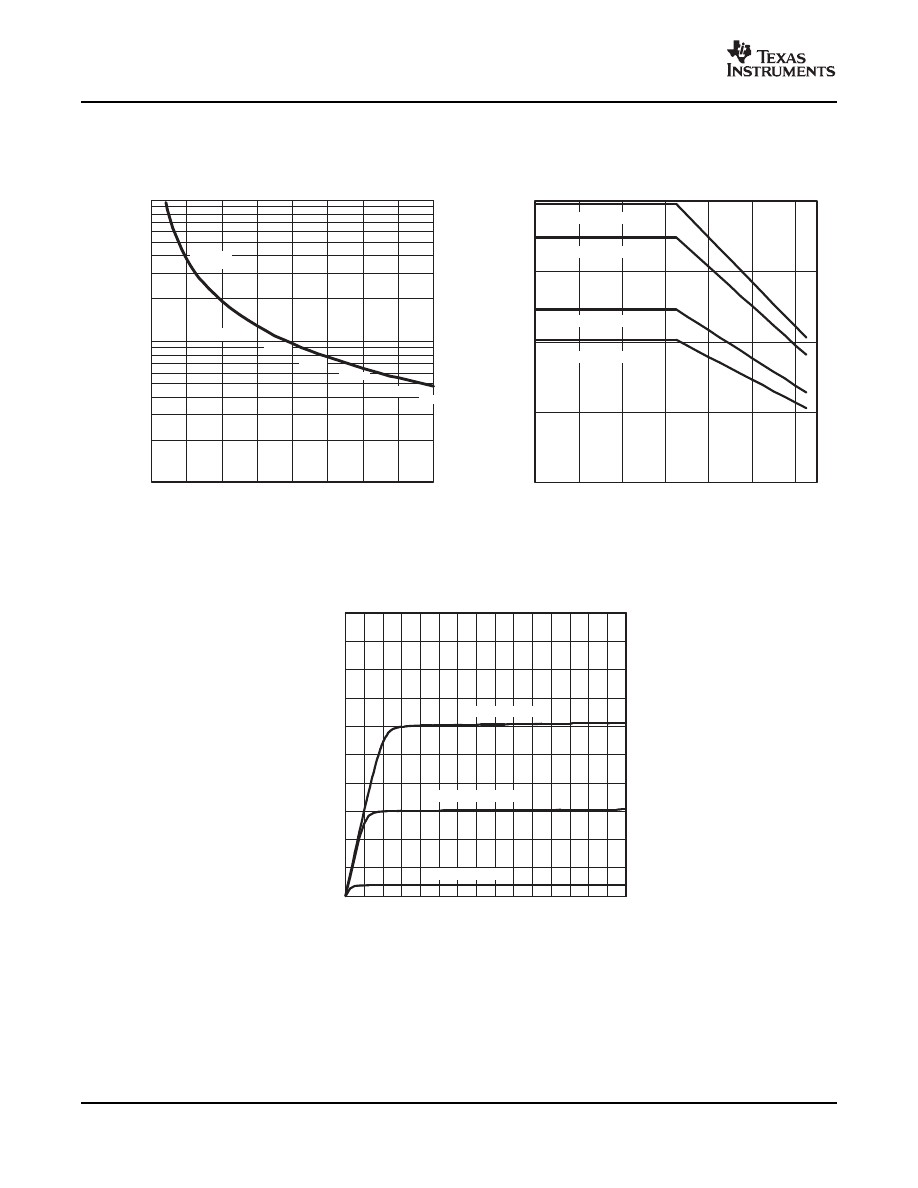
Typical Characteristics
T
A
− Free-Air Temperature −
5
C
0
1000
2000
3000
4000
−40
−20
0
20
40
60
80
Power Dissipation Rate − mW
TLC5941PWP+
TLC5941RHB
TLC5941NT
TLC5941PWP−
100
0
10
20
30
40
50
60
70
80
R
(IREF)
−
ReferenceResistor
−
1 k
10 k
3.84 k
1.92 k
1.28 k
0.96 k
0.79 k
0.64 k
0.55 k
0.48 k
I
O(LC)
− Output Current − mA
0
10
20
30
40
50
60
70
80
90
100
0 0.2 0.4 0.6 0.8 1 1.2 1.4 1.61.8 2 2.2 2.4 2.6 2.8 3
I
MAX
= 60 mA
I
MAX
= 30 mA
I
MAX
= 5 mA
I O
− Output Current − mA
V
O
− Output Voltage − V
SLVS589B – JULY 2005 – REVISED APRIL 2007
REFERENCE RESISTOR
POWER DISSIPATION RATE
vs
vs
OUTPUT CURRENT
FREE-AIR TEMPERATURE
Figure 3.
Figure 4.
OUTPUT CURRENT
vs
OUTPUT VOLTAGE
Figure 5.
10
www.ti.com
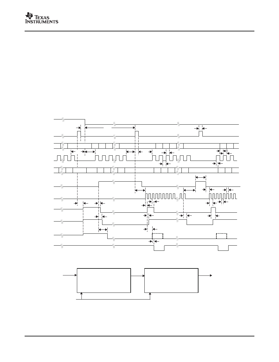
PRINCIPLES OF OPERATION
SERIAL INTERFACE
MODE
XLAT
SIN
SCLK
SOUT
BLANK
GSCLK
OUT0
(current)
OUT1
(current)
OUT15
(current)
XERR
1
96
DC
MSB
DC
LSB
DC
MSB
1
192
193
1
192
193
1
1
4096
tsu4
th4
twh3
1
GS1
MSB
GS1
LSB
GS1
MSB
GS2
MSB
GS2
LSB
GS2
MSB
SID2
MSB
SID2
MSB-1
SID1
MSB
SID1
MSB-1
SID1
LSB
GS3
MSB
-
-
-
twh2
tsu2
tsu1
twh0
twl0
tsu0
th0
tpd0
tpd1
t
+ t
pd1
d
t
+ 15 x t
pd1
d
tpd3
td
15 x td
tpd2
t
+ t
pd3
d
tpd3
tpd4
twl1
twh1
DC Data Input Mode
GS Data Input Mode
1st GS Data Input Cycle
2nd GS Data Input Cycle
1st GS Data Output Cycle
2nd GS Data Output Cycle
tsu3
th3
th2
th1
tsu5
Tgsclk
touton
SIN
SOUT
SIN(a)
SOUT(b )
TLC5941 (a)
GSCLK,
BLANK,
SIN
SOUT
TLC5941 (b)
SCLK, XLAT,
MODE
SLVS589B – JULY 2005 – REVISED APRIL 2007
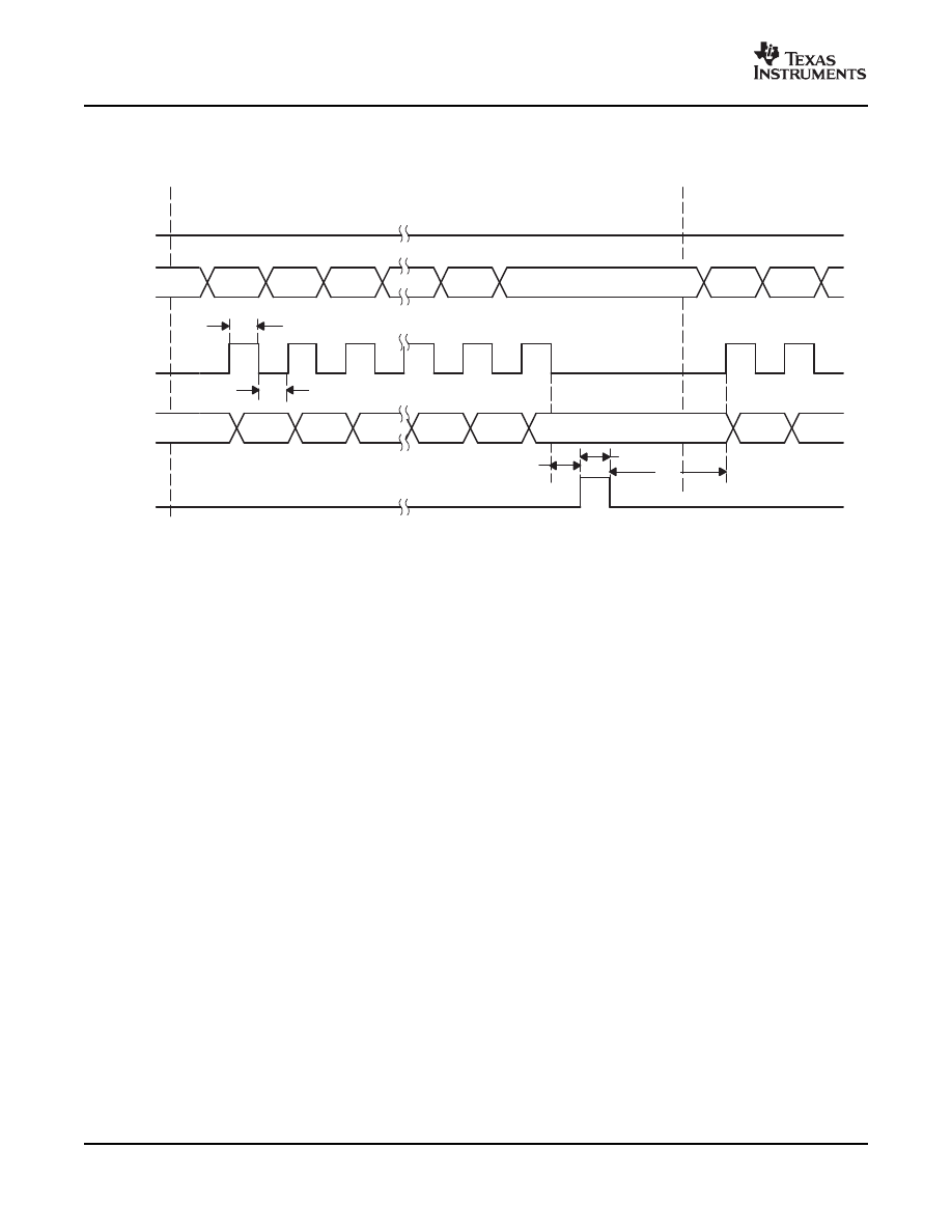
The TLC5941 has a flexible serial interface, which can be connected to microcontrollers or digital signal
processors in various ways. Only 3 pins are needed to input data into the device. The rising edge of SCLK
signal shifts the data from the SIN pin to the internal register. After all data is clocked in, a high-level pulse of
XLAT signal latches the serial data to the internal registers. The internal registers are level-triggered latches of
XLAT signal. All data are clocked in with the MSB first. The length of serial data is 96 bit or 192 bit, depending
on the programming mode. Grayscale data and dot correction data can be entered during a grayscale cycle.
Although new grayscale data can be clocked in during a grayscale cycle, the XLAT signal should only latch the
grayscale data at the end of the grayscale cycle. Latching in new grayscale data immediately overwrites the
existing grayscale data.
shows the timing chart. More than two TLC5941s can be connected in series
by connecting an SOUT pin from one device to the SIN pin of the next device. An example of cascading two
TLC5941s is shown in
. The SOUT pin can also be connected to the controller to receive status
information from TLC5941 as shown in
.
Figure 6. Serial Data Input Timing Chart
Figure 7. Cascading Two TLC5941 Devices
11
www.ti.com
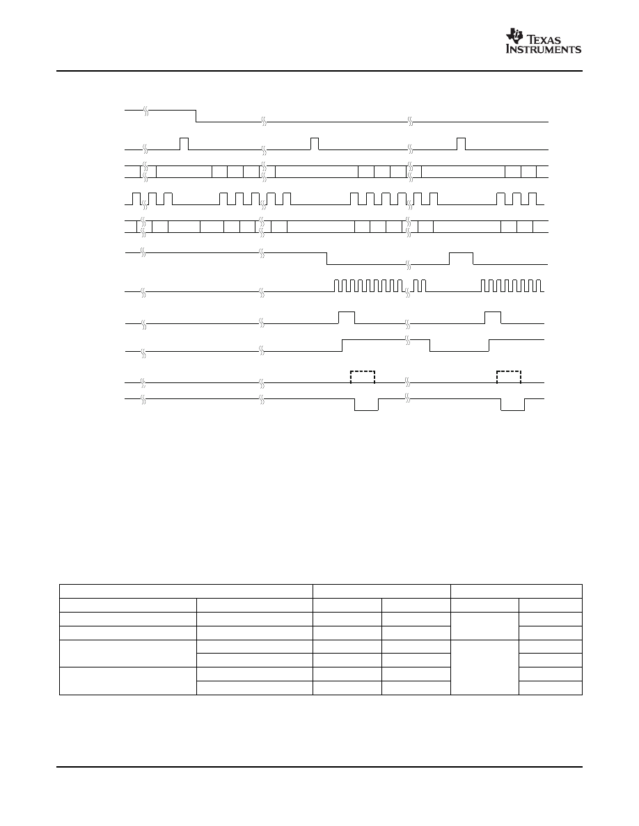
MODE
XLAT
SIN(a
)
SCLK
SOUT(b
)
BLANK
GSCLK
OUT0
(current)
OUT1
(current)
OUT15
(current)
XERR
1
192X2
DCb
MSB
DCa
LSB
DCb
MSB
1
384
385
1
384
385
1
1
4096
1
GSb1
MSB
GSa1
LSB
GSb1
MSB
GSb2
MSB
GSa2
LSB
GSb2
MSB
SIDb2
MSB
SIDb2
MSB
-1
SIDb1
MSB
SIDb1
MSB-1
SIDa1
LSB
GSb3
MSB
-
-
-
192
96X2
ERROR INFORMATION OUTPUT
SLVS589B – JULY 2005 – REVISED APRIL 2007
PRINCIPLES OF OPERATION (continued)
Figure 8. Timing Chart for Two Cascaded TLC5941 Devices
The open-drain output XERR is used to report both of the TLC5941 error flags, TEF and LOD. During normal
operating conditions, the internal transistor connected to the XERR pin is turned off. The voltage on XERR is
pulled up to V
CC
through an external pullup resistor. If TEF or LOD is detected, the internal transistor is turned
on, and XERR is pulled to GND. Because XERR is an open-drain output, multiple ICs can be ORed together
and pulled up to V
CC
with a single pullup resistor. This reduces the number of signals needed to report a system
error (see
).
To differentiate LOD and TEF signal from XERR pin, LOD can be masked out with BLANK = HIGH.
Table 2. XERR Truth Table
ERROR CONDITION
ERROR INFORMATION
SIGNALS
TEMPERATURE
OUTn VOLTAGE
TEF
LOD
BLANK
XERR
T
J
< T
(TEF)
Don't Care
L
X
H
H
T
J
> T
(TEF)
Don't Care
H
X
L
OUTn > V
(LED)
L
L
H
T
J
< T
(TEF)
OUTn < V
(LED)
L
H
L
L
OUTn > V
(LED)
H
L
L
T
J
> T
(TEF)
OUTn < V
(LED)
H
H
L
12
www.ti.com
TEF: THERMAL ERROR FLAG
LOD: LED OPEN DETECTION
DELAY BETWEEN OUTPUTS
OUTPUT ENABLE
SLVS589B – JULY 2005 – REVISED APRIL 2007
The TLC5941 provides a temperature error flag (TEF) circuit to indicate an overtemperature condition of the IC.
If the junction temperature exceeds the threshold temperature (160°C typical), TEF becomes H and XERR pin
goes to low level. When the junction temperature becomes lower than the threshold temperature, TEF becomes
L and XERR pin becomes high impedance. TEF status can also be read out from the TLC5941 status register.
The TLC5941 has an LED-open detection circuit that detects broken or disconnected LED's. The LED open
detector pulls the XERR pin to GND when an open LED is detected. XERR and the corresponding error bit in
the Status Information Data is only active under the following open LED conditions.
1. OUTn is on and the time tpd2 (1
µ
s typical) has passed.
2. The voltage of OUTn is < 0.3V (typical)
The LOD status of each output can be also read out from the SOUT pin. See the
section for details. The LOD error bits are latched into the Status Information Data when XLAT returns
to a low after a high. Therefore, the XLAT pin must be pulsed high then low while XERR is active in order to
latch the LOD error into the Status Information Data for subsequent reading via the serial shift register.
The TLC5941 has graduated delay circuits between outputs. These circuits can be found in the constant current
driver block of the device (see the functional block diagram). The fixed-delay time is 20ns (typical), OUT0 has no
delay, OUT1 has 20ns delay, and OUT2 has 40ns delay, etc. The maximum delay is 300ns from OUT0 to
OUT15. The delay works during switch on and switch off of each output channel. These delays prevent large
inrush currents which reduces the bypass capacitors when the outputs turn on.
All OUTn channels of the TLC5941 can be switched off with one signal. When BLANK is set high, all OUTn
channels are disabled, regardless of logic operations of the device. The grayscale counter is also reset. When
BLANK is set low, all OUTn channels work under normal conditions. If BLANK goes low and then back high
again in less than 300ns, all outputs programmed to turn on still turn on for either the programmed number of
grayscale clocks, or the length of time that the BLANK signal was low, which ever is lower. For example, if all
outputs are programmed to turn on for 1ms, but the BLANK signal is only low for 200ns, all outputs still turn on
for 200ns, even though some outputs are turning on after the BLANK signal has already gone high.
Table 3. BLANK Signal Truth Table
BLANK
OUT0 - OUT15
LOW
Normal condition
HIGH
Disabled
13
www.ti.com
SETTING MAXIMUM CHANNEL CURRENT
Imax
+
V
(IREF)
R
(IREF)
31.5
(6)
POWER DISSIPATION CALCULATION
P
D
+
ǒ
V
CC
I
CC
Ǔ
)
ǒ
V
OUT
I
MAX
N
DCn
63
d
PWM
Ǔ
(7)
OPERATING MODES
SLVS589B – JULY 2005 – REVISED APRIL 2007
The maximum output current per channel is programmed by a single resistor, R
(IREF)
, which is placed between
IREF pin and GND pin. The voltage on IREF is set by an internal band gap V
(IREF)
with a typical value of
1.24 V. The maximum channel current is equivalent to the current flowing through R
(IREF)
multiplied by a factor of
31.5. The maximum output current can be calculated by
:
where:
V
(IREF)
= 1.24 V
R
(IREF)
= User-selected external resistor.
I
max
must be set between 5 mA and 80 mA. The output current may be unstable if I
max
is set lower than 5 mA.
Output currents lower than 5 mA can be achieved by setting Imax to 5 mA or higher and then using dot
correction.
shows the maximum output current I
O
versus R
(IREF)
. R
(IREF)
is the value of the resistor between IREF
terminal to GND, and I
O
is the constant output current of OUT0 to OUT15. A variable power supply may be
connected to the IREF pin through a resistor to change the maximum output current per channel. The maximum
output current per channel is 31.5 times the current flowing out of the IREF pin.
The device power dissipation needs to be below the power dissipation rate of the device package to ensure
correct operation.
calculates the power dissipation of device:
where:
V
CC
: device supply voltage
I
CC
: device supply current
V
OUT
: TLC5941 OUTn voltage when driving LED current
I
MAX
: LED current adjusted by R
(IREF)
Resistor
DC
n
: maximum dot correction value for OUTn
N: number of OUTn driving LED at the same time
d
PWM
: duty cycle defined by BLANK pin or GS PWM value
The TLC5941 has two operating modes defined by MODE as shown in
. The GS and DC registers are
set to random values that are not known just after power on. The GS and DC values must be programmed
before turning on the outputs. Please note that when initially setting GS and DC data after power on, the GS
data must be set before the DC data is set. Failure to set GS data before DC data may result in the first bit of
GS data being lost. XLAT must be low when the MODE pin goes high-to-low or low-to-high to change back and
forth between GS mode and DC mode.
Table 4. TLC5941 Operating Modes Truth Table
MODE
INPUT SHIFT REGISTER
OPERATING MODE
GND
192 bit
Grayscale PWM Mode
V
CC
96 bit
Dot Correction Data Input Mode
14
www.ti.com
SETTING DOT CORRECTION
I
OUTn
+
Imax
DCn
63
(8)
DC 0.0
95
DC 1.0
89
DC 15.0
5
DC 15.5
0
DC 0.5
90
DC 14.5
6
MSB
LSB
DC OUT15
DC OUT0
DC OUT14 − DC OUT1
SLVS589B – JULY 2005 – REVISED APRIL 2007
The TLC5941 has the capability to fine-adjust the output current of each channel (OUT0 to OUT15)
independently. This is also called dot correction. This feature is used to adjust the brightness deviations of LEDs
connected to the output channels OUT0 to OUT15. Each of the 16 channels can be programmed with a 6-bit
word. The channel output can be adjusted in 64 steps from 0% to 100% of the maximum output current I
max
. The
TEST pin must be connected to VCC to ensure proper operation of the dot correction circuitry.
determines the output current for each output n:
where:
I
max
= the maximum programmable output current for each output.
DCn = the programmed dot correction value for output n (DCn = 0 to 63).
n = 0 to 15
shows the dot correction data packet format which consists of 6 bits x 16 channel, total 96 bits. The
format is Big-Endian format. This means that the MSB is transmitted first, followed by the MSB-1, etc. The DC
15.5 in
stands for the 5
th
-most significant bit for output 15.
Figure 9. Dot Correction Data Packet Format
When MODE is set to VCC, the TLC5941 enters the dot correction data input mode. The length of input shift
register becomes 96bits. After all serial data are shifted in, the TLC5941 writes the data in the input shift register
to DC register when XLAT is high, and holds the data in the DC register when XLAT is low. The DC register is a
level triggered latch of XLAT signal. Since XLAT is a level-triggered signal, SCLK and SIN must not be changed
while XLAT is high. After XLAT goes low, data in the DC register is latched and does not change. BLANK signal
does not need to be high to latch in new data. When XLAT goes high, the new dot-correction data immediately
becomes valid and changes the output currents if BLANK is low. XLAT has setup time (tsu1) and hold time (th1)
to SCLK as shown in
.
15
www.ti.com
t
su1
DC n
MSB
DC n
MSB−1
DC n
MSB−2
DC n
LSB+1
DC n
LSB
DC n
MSB
DC n+1
MSB
DC n+1
MSB−1
DC n
MSB−1
DC n
MSB−2
DC n−1
LSB
DC n−1
LSB+1
DC n−1
MSB
DC n−1
MSB−1
DC n−1
MSB−2
1
2
3
95
96
1
2
SCLK
SOUT
SIN
MODE
XLAT
DC Mode Data
Input Cycle n
DC Mode Data
Input Cycle n+1
V
CC
t
wh0
t
wl0
DC n−1
LSB
t
wh2
t
h1
SLVS589B – JULY 2005 – REVISED APRIL 2007
To input data into the dot correction register, MODE must be set to V
CC
. The internal input shift register is then
set to 96-bit width. After all serial data are clocked in, a rising edge of XLAT is used to latch the data into the dot
correction register.
shows the dc data input timing chart.
Figure 10. Dot Correction Data Input Timing Chart
16
www.ti.com
SETTING GRAYSCALE
Brightness in %
+
GSn
4095
100
(9)
GS 0.0
191
GS 1.0
179
GS 15.0
11
GS 15.11
0
GS 0.11
180
GS 14.11
12
MSB
LSB
GS OUT15
GS OUT0
GS OUT14 − GS OUT1
t
su2
SCLK
SOUT
SIN
MODE
GS
MSB
1
Following GS Mode Data
Input Cycle
XLAT
DC
LSB
96
DC Mode Data
Input Cycle
192
GS
LSB
193
GS + 1
MSB
1
DC n
LSB
DC
MSB
GS
MSB
SID
MSB
SID
MSB−1
First GS Mode Data
Input Cycle After DC Data Input Cycle
192
SID n + 1
MSB
GS n + 1
LSB
t
h3
t
su3
t
h1
t
h2
t
su1
t
wh2
t
h3
X
X
SID
LSB
t
pd0
SLVS589B – JULY 2005 – REVISED APRIL 2007
The TLC5941 can adjust the brightness of each channel OUTn using a PWM control scheme. The use of 12 bits
per channel results in 4096 different brightness steps, from 0% to 100% brightness.
determines the
brightness level for each output n:
where:
GSn = the programmed grayscale value for output n (GSn = 0 to 4095)
n = 0 to 15
Grayscale data for all OUTn
The input shift register enters grayscale data into the grayscale register for all channels simultaneously. The
complete grayscale data format consists of 16 x 12 bit words, which forms a 192-bit wide data packet (see
). The data packet must be clocked in with the MSB first.
Figure 11. Grayscale Data Packet Format
When MODE is set to GND, the TLC5941 enters the grayscale data input mode. The device switches the input
shift register to 192-bit width. After all data is clocked in, a rising edge of the XLAT signal latches the data into
the grayscale register (see
). New grayscale data immediately becomes valid at the rising edge of the
XLAT signal; therefore, new grayscale data should be latched at the end of a grayscale cycle when BLANK is
high. The first GS data input cycle after dot correction requires an additional SCLK pulse after the XLAT signal
to complete the grayscale update cycle. All GS data in the input shift register is replaced with status information
data (SID) after updating the grayscale register.
Figure 12. Grayscale Data Input Timing Chart
17
www.ti.com
STATUS INFORMATION OUTPUT
X
X
TEF
X
X
DC 0.0
DC 15.5
LOD 0
LOD 15
191
120
119
24
23
16
15
0
LSB
MSB
Reserved
TEF
DC Values
LOD Data
SLVS589B – JULY 2005 – REVISED APRIL 2007
The TLC5941 does have a status information register, which can be accessed in grayscale mode (MODE =
GND). After the XLAT signal latches the data into the GS register, the input shift register data is replaced with
status information data (SID) of the device (see
). LOD, TEF, and dot-correction register data can be
read out at the SOUT pin. The status information data packet is 192 bits wide. Bits 0 – 15 contain the LOD
status of each channel. Bit 16 contains the TEF status. Bits 24 – 119 contain the data of the dot-correction
register. The remaining bits are reserved. The complete status information data packet is shown in
SOUT outputs the MSB of the SID at the same time the SID are stored in the SID register, as shown in
. The next SCLK pulse, which will be the clock for receiving the MSB of the next grayscale data,
transmits MSB-1 of SID. If output voltage is < 0.3 V (typical) when the output sink current turns on, LOD status
flag becomes active. The LOD status flag is an internal signal which pulls XERR pin down to low when the LOD
status flag becomes active. The delay time, tpd2 (1
µ
s maximum), is from the time of turning on the output sink
current to the time LOD status flag becomes valid. The timing for each channels LOD status to become valid is
shifted by the 30-ns (maximum), channel-to-channel turn-on time. After the first GSCLK goes high, OUT0 LOD
status is valid; tpd3 + tpd2 = 60 nS + 1
µ
s = 1.06
µ
s. OUT1 LOD status is valid; tpd3 + td + tpd2 = 60 ns + 30 ns
+ 1
µ
s = 1.09
µ
s. OUT2 LOD status is valid; tpd3 + 2*td + tpd2 = 1.12
µ
s, and so on. It takes 1.51
µ
s maximum
(tpd3 + 15*td + tpd2) from the first GSCLK rising edge until all LOD become valid; tsuLOD must be > 1.51
µ
s
(see
) to ensure that all LOD data are valid.
Figure 13. Status Information Data Packet Format
18
www.ti.com
MODE
XLAT
SIN
SCLK
SOUT
BLANK
GSCLK
OUT0
(current)
OUT1
(current)
OUT15
(current)
XERR
1
192
193
1
192
1
4096
GS1
MSB
GS1
LSB
GS1
MSB
GS2
MSB
GS2
LSB
GS2
MSB
SID1
MSB
SID1
MSB-1
SID1
LSB
-
-
t
+ 15 x t + t
pd3
d
pd2
tpd3
td
15 x td
tpd2
GS Data Input Mode
1st GS Data Input Cycle
2nd GS Data Input Cycle
(1st GS Data Output Cycle)
tsuLOD
t
suLOD
pd3
d
> t
+ t
15 + t
´
pd2
SLVS589B – JULY 2005 – REVISED APRIL 2007
Figure 14. Readout Status Information Data (SID) Timing Chart
The LOD status of each output can be read out from the SOUT pin. The LOD error bits are latched into the
Status Information Data when XLAT returns to a low after a high. Therefore, the XLAT pin must be pulsed high
then low while XERR is active in order to latch the LOD error into the Status Information Data for subsequent
reading via the serial shift register.
19
www.ti.com
GRAYSCALE PWM OPERATION
GSCLK
BLANK
GS PWM
Cycle n
1
2
3
1
GS PWM
Cycle n+1
OUT0
OUT1
OUT15
XERR
n x t
d
t
pd1
t
pd1
+ t
d
t
pd1
+ 15 x t
d
t
pd2
t
pd3
t
wh1
t
wl1
t
wl1
t
pd3
4096
t
h4
t
wh3
t
pd3
+ n x t
d
t
su4
(Current)
(Current)
(Current)
Output On Time
)
GSCLK
(
n
f
GSn
on
_
T
err
_
on
t
+
=
(10)
SLVS589B – JULY 2005 – REVISED APRIL 2007
The grayscale PWM cycle starts with the falling edge of BLANK. The first GSCLK pulse after BLANK goes low
increases the grayscale counter by one and switches on all OUTn with grayscale value not zero. Each following
rising edge of GSCLK increases the grayscale counter by one. The TLC5941 compares the grayscale value of
each output OUTn with the grayscale counter value. All OUTn with grayscale values equal to the counter values
are switched off. A BLANK=H signal after 4096 GSCLK pulses resets the grayscale counter to zero and
completes the grayscale PWM cycle (see
). When the counter reaches a count of FFFh, the counter
stops counting and all outputs turn off. Pulling BLANK high before the counter reaches FFFh immediately resets
the counter to zero.
Figure 15. Grayscale PWM Cycle Timing Chart
The amount of time that each output is turned on is a function of the grayscale clock frequency and the
programmed grayscale PWM value. The on-time of each output can be calculated using
.
Where
•
T_on
n
is the time that OUTn turns on and sinks current
•
GSn is OUTn's programmed grayscale PWM value between 0 and 4095
•
t
on_err
is the Output on time error defined in the Switching Characteristics Table
When using
with very high GSCLK frequencies and very low grayscale PWM values, the resulting
T_on time may be negative. If T_on is negative, the output does not turn on. For example, using f(GSCLK) = 30
MHz, GSn = 1, and the typical t
on_err
= 50 nS,
calculates that OUTn turns on for –16.6 nS. This
output may not turn on under these conditions. Increasing the PWM value or reducing the GSCLK clock
frequency guarantees turn-on.
20
www.ti.com
SERIAL DATA TRANSFER RATE
f
(GSCLK)
+
4096
f
(update)
f
(SCLK)
+
193
f
(update)
n
(11)
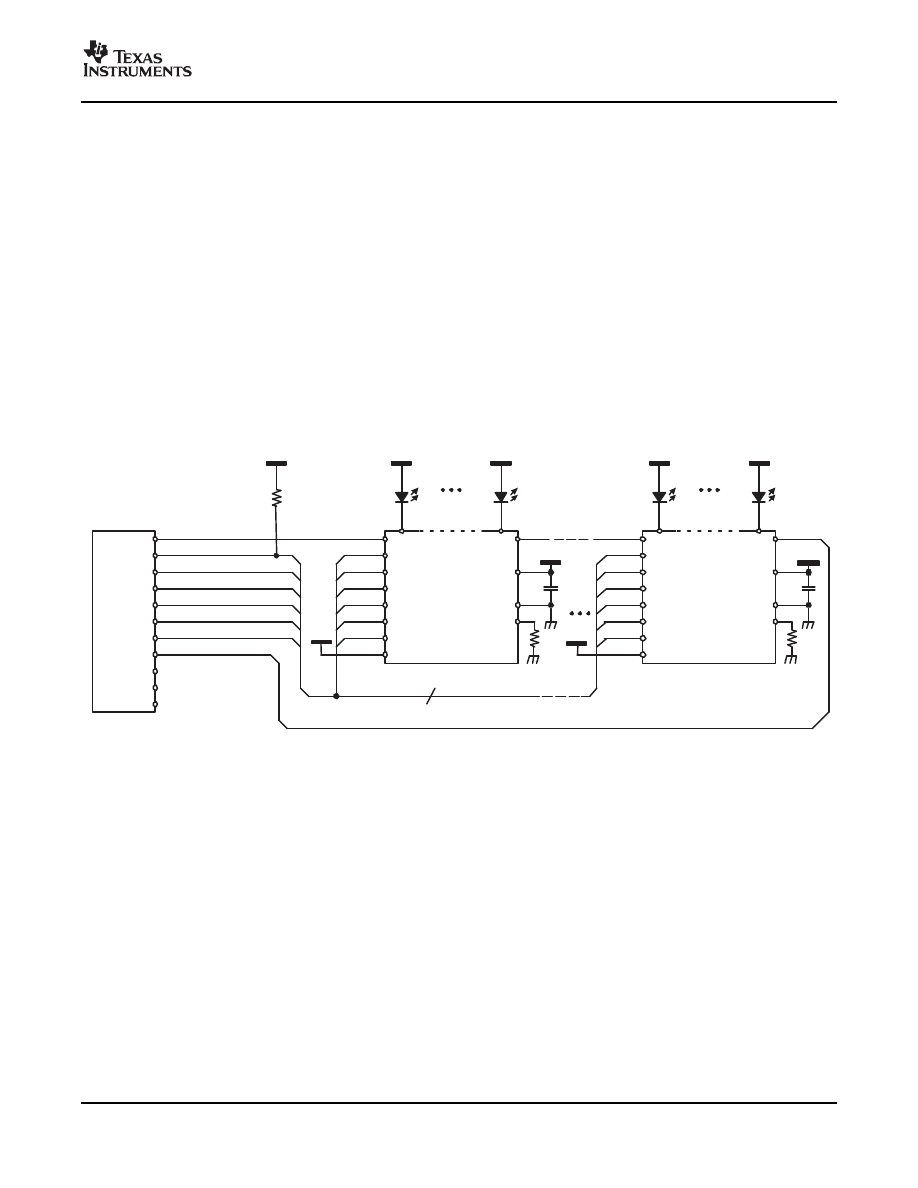
Application Example
TLC5941
SIN
SOUT
OUT0
OUT15
SCLK
GSCLK
XLAT
TEST
BLANK
IREF
XERR
MODE
TLC5941
SIN
SOUT
OUT0
OUT15
SCLK
GSCLK
XLAT
TEST
BLANK
IREF
XERR
MODE
IC 0
IC n
6
SIN
SCLK
GSCLK
XLAT
BLANK
XERR
MODE
Controller
SOUT
100 k
100 nF
V(LED)
V(LED)
V(LED)
V(LED)
VCC
100 nF
VCC
VCC
VCC
VCC
SLVS589B – JULY 2005 – REVISED APRIL 2007
shows a cascading connection of n TLC5941 devices connected to a controller, building a basic
module of an LED display system. There is no TLC5941 limitation to the maximum number of ICs that can be
cascaded. The maximum number of cascading TLC5941 devices depends on the application system and is in
the range of 40 devices.
calculates the minimum frequency needed:
where:
f
(GSCLK)
: minimum frequency needed for GSCLK
f
(SCLK)
: minimum frequency needed for SCLK and SIN
f
(update)
: update rate of whole cascading system
n: number cascaded of TLC5941 device
Figure 16. Cascading Devices
21
PACKAGING INFORMATION
Orderable Device
Status
(1)
Package
Type
Package
Drawing
Pins Package
Qty
Eco Plan
(2)
Lead/Ball Finish
MSL Peak Temp
(3)
TLC5941PWP
ACTIVE
HTSSOP
PWP
28
50
Green (RoHS &
no Sb/Br)
CU NIPDAU
Level-2-260C-1 YEAR
TLC5941PWPG4
ACTIVE
HTSSOP
PWP
28
50
Green (RoHS &
no Sb/Br)
CU NIPDAU
Level-2-260C-1 YEAR
TLC5941PWPR
ACTIVE
HTSSOP
PWP
28
2000 Green (RoHS &
no Sb/Br)
CU NIPDAU
Level-2-260C-1 YEAR
TLC5941PWPRG4
ACTIVE
HTSSOP
PWP
28
2000 Green (RoHS &
no Sb/Br)
CU NIPDAU
Level-2-260C-1 YEAR
TLC5941RHBR
ACTIVE
QFN
RHB
32
3000 Green (RoHS &
no Sb/Br)
CU NIPDAU
Level-2-260C-1 YEAR
TLC5941RHBRG4
ACTIVE
QFN
RHB
32
3000 Green (RoHS &
no Sb/Br)
CU NIPDAU
Level-2-260C-1 YEAR
TLC5941RHBT
ACTIVE
QFN
RHB
32
250
Green (RoHS &
no Sb/Br)
CU NIPDAU
Level-2-260C-1 YEAR
TLC5941RHBTG4
ACTIVE
QFN
RHB
32
250
Green (RoHS &
no Sb/Br)
CU NIPDAU
Level-2-260C-1 YEAR
(1)
The marketing status values are defined as follows:
ACTIVE: Product device recommended for new designs.
LIFEBUY: TI has announced that the device will be discontinued, and a lifetime-buy period is in effect.
NRND: Not recommended for new designs. Device is in production to support existing customers, but TI does not recommend using this part in
a new design.
PREVIEW: Device has been announced but is not in production. Samples may or may not be available.
OBSOLETE: TI has discontinued the production of the device.
(2)
Eco Plan - The planned eco-friendly classification: Pb-Free (RoHS), Pb-Free (RoHS Exempt), or Green (RoHS & no Sb/Br) - please check
http://www.ti.com/productcontent
for the latest availability information and additional product content details.
TBD: The Pb-Free/Green conversion plan has not been defined.
Pb-Free (RoHS): TI's terms "Lead-Free" or "Pb-Free" mean semiconductor products that are compatible with the current RoHS requirements
for all 6 substances, including the requirement that lead not exceed 0.1% by weight in homogeneous materials. Where designed to be soldered
at high temperatures, TI Pb-Free products are suitable for use in specified lead-free processes.
Pb-Free (RoHS Exempt): This component has a RoHS exemption for either 1) lead-based flip-chip solder bumps used between the die and
package, or 2) lead-based die adhesive used between the die and leadframe. The component is otherwise considered Pb-Free (RoHS
compatible) as defined above.
Green (RoHS & no Sb/Br): TI defines "Green" to mean Pb-Free (RoHS compatible), and free of Bromine (Br) and Antimony (Sb) based flame
retardants (Br or Sb do not exceed 0.1% by weight in homogeneous material)
(3)
MSL, Peak Temp. -- The Moisture Sensitivity Level rating according to the JEDEC industry standard classifications, and peak solder
temperature.
Important Information and Disclaimer:The information provided on this page represents TI's knowledge and belief as of the date that it is
provided. TI bases its knowledge and belief on information provided by third parties, and makes no representation or warranty as to the
accuracy of such information. Efforts are underway to better integrate information from third parties. TI has taken and continues to take
reasonable steps to provide representative and accurate information but may not have conducted destructive testing or chemical analysis on
incoming materials and chemicals. TI and TI suppliers consider certain information to be proprietary, and thus CAS numbers and other limited
information may not be available for release.
In no event shall TI's liability arising out of such information exceed the total purchase price of the TI part(s) at issue in this document sold by TI
to Customer on an annual basis.
PACKAGE OPTION ADDENDUM
www.ti.com
14-Feb-2007
Addendum-Page 1
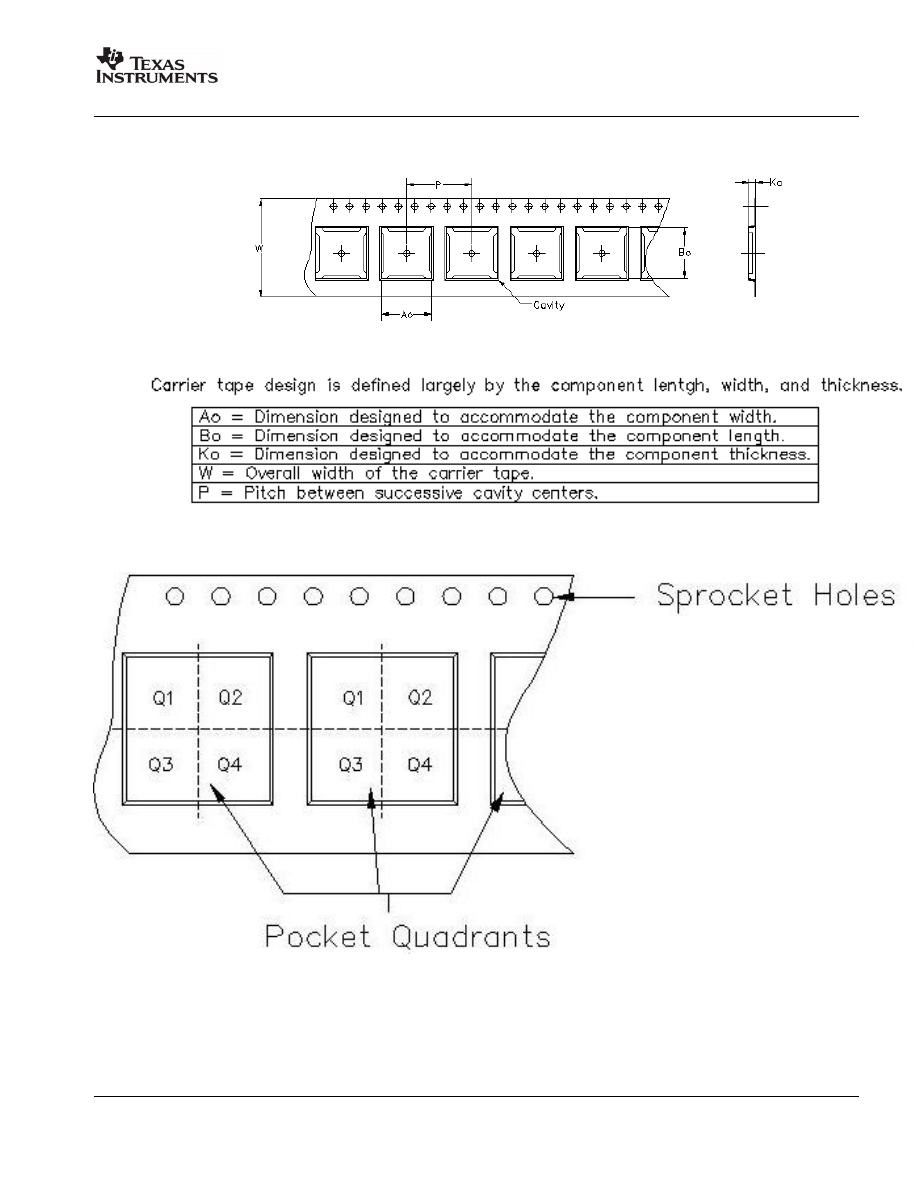
TAPE AND REEL INFORMATION
PACKAGE MATERIALS INFORMATION
www.ti.com
21-Jul-2007
Pack Materials-Page 1
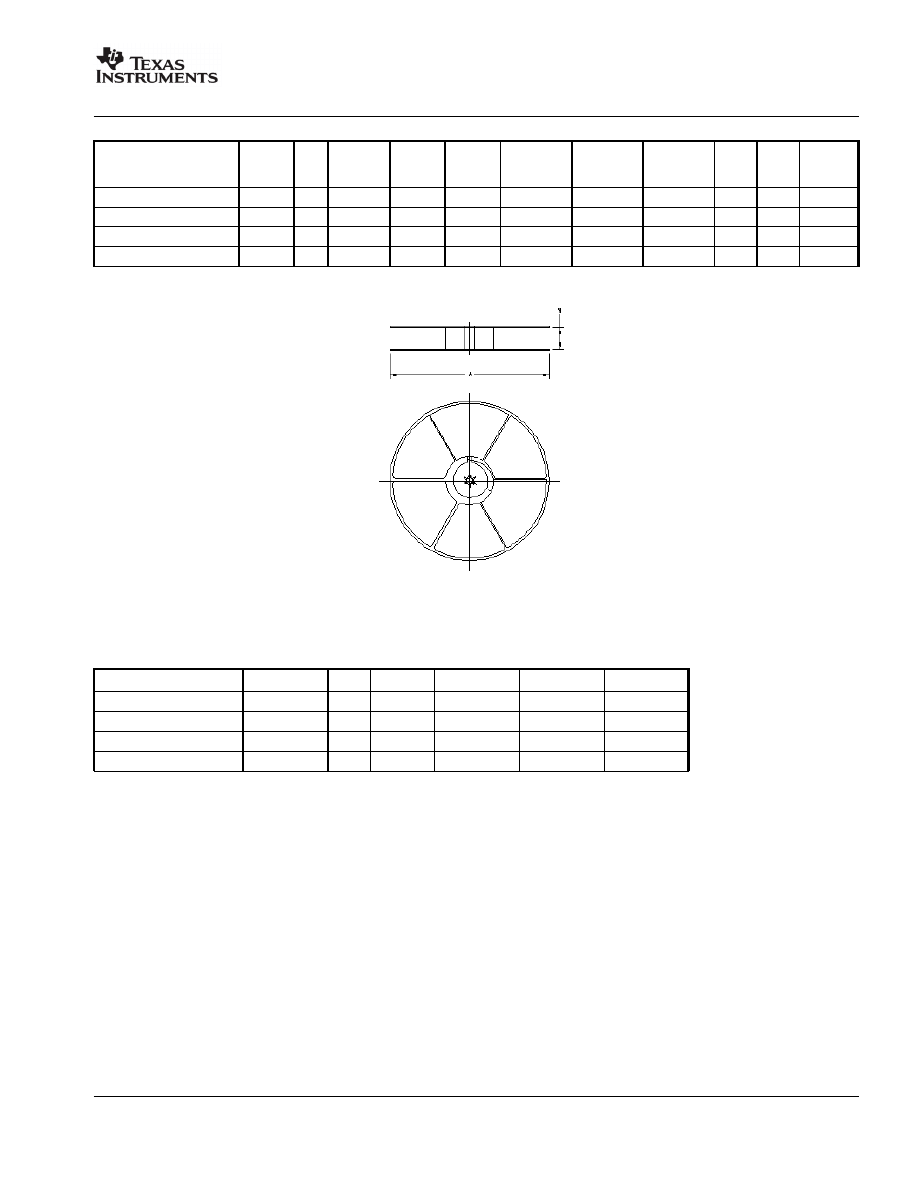
Device
Package Pins
Site
Reel
Diameter
(mm)
Reel
Width
(mm)
A0 (mm)
B0 (mm)
K0 (mm)
P1
(mm)
W
(mm)
Pin1
Quadrant
TLC5941PWPR
PWP
28
TAI
330
16
6.9
10.2
1.8
12
16
Q1
TLC5941PWPR
PWP
28
MLA
330
16
7.1
10.4
1.6
12
16
Q1
TLC5941RHBR
RHB
32
MLA
330
12
5.3
5.3
1.5
8
12
Q2
TLC5941RHBT
RHB
32
MLA
180
12
5.3
5.3
1.5
8
12
Q2
TAPE AND REEL BOX INFORMATION
Device
Package
Pins
Site
Length (mm)
Width (mm)
Height (mm)
TLC5941PWPR
PWP
28
TAI
535.4
167.7
48.3
TLC5941PWPR
PWP
28
MLA
346.0
346.0
33.0
TLC5941RHBR
RHB
32
MLA
346.0
346.0
29.0
TLC5941RHBT
RHB
32
MLA
552.0
212.7
36.0
PACKAGE MATERIALS INFORMATION
www.ti.com
21-Jul-2007
Pack Materials-Page 2
PACKAGE MATERIALS INFORMATION
www.ti.com
21-Jul-2007
Pack Materials-Page 3

IMPORTANT NOTICE
Texas Instruments Incorporated and its subsidiaries (TI) reserve the right to make corrections, modifications, enhancements,
improvements, and other changes to its products and services at any time and to discontinue any product or service without notice.
Customers should obtain the latest relevant information before placing orders and should verify that such information is current and
complete. All products are sold subject to TI’s terms and conditions of sale supplied at the time of order acknowledgment.
TI warrants performance of its hardware products to the specifications applicable at the time of sale in accordance with TI’s
standard warranty. Testing and other quality control techniques are used to the extent TI deems necessary to support this
warranty. Except where mandated by government requirements, testing of all parameters of each product is not necessarily
performed.
TI assumes no liability for applications assistance or customer product design. Customers are responsible for their products and
applications using TI components. To minimize the risks associated with customer products and applications, customers should
provide adequate design and operating safeguards.
TI does not warrant or represent that any license, either express or implied, is granted under any TI patent right, copyright, mask
work right, or other TI intellectual property right relating to any combination, machine, or process in which TI products or services
are used. Information published by TI regarding third-party products or services does not constitute a license from TI to use such
products or services or a warranty or endorsement thereof. Use of such information may require a license from a third party under
the patents or other intellectual property of the third party, or a license from TI under the patents or other intellectual property of TI.
Reproduction of TI information in TI data books or data sheets is permissible only if reproduction is without alteration and is
accompanied by all associated warranties, conditions, limitations, and notices. Reproduction of this information with alteration is an
unfair and deceptive business practice. TI is not responsible or liable for such altered documentation. Information of third parties
may be subject to additional restrictions.
Resale of TI products or services with statements different from or beyond the parameters stated by TI for that product or service
voids all express and any implied warranties for the associated TI product or service and is an unfair and deceptive business
practice. TI is not responsible or liable for any such statements.
TI products are not authorized for use in safety-critical applications (such as life support) where a failure of the TI product would
reasonably be expected to cause severe personal injury or death, unless officers of the parties have executed an agreement
specifically governing such use. Buyers represent that they have all necessary expertise in the safety and regulatory ramifications
of their applications, and acknowledge and agree that they are solely responsible for all legal, regulatory and safety-related
requirements concerning their products and any use of TI products in such safety-critical applications, notwithstanding any
applications-related information or support that may be provided by TI. Further, Buyers must fully indemnify TI and its
representatives against any damages arising out of the use of TI products in such safety-critical applications.
TI products are neither designed nor intended for use in military/aerospace applications or environments unless the TI products are
specifically designated by TI as military-grade or "enhanced plastic." Only products designated by TI as military-grade meet military
specifications. Buyers acknowledge and agree that any such use of TI products which TI has not designated as military-grade is
solely at the Buyer's risk, and that they are solely responsible for compliance with all legal and regulatory requirements in
connection with such use.
TI products are neither designed nor intended for use in automotive applications or environments unless the specific TI products
are designated by TI as compliant with ISO/TS 16949 requirements. Buyers acknowledge and agree that, if they use any
non-designated products in automotive applications, TI will not be responsible for any failure to meet such requirements.
Following are URLs where you can obtain information on other Texas Instruments products and application solutions:
Products
Applications
Amplifiers
Audio
Data Converters
Automotive
DSP
Broadband
Interface
Digital Control
Logic
Military
Power Mgmt
Optical Networking
Microcontrollers
Security
RFID
Telephony
Low Power
Video & Imaging
Wireless
Wireless
Mailing Address: Texas Instruments, Post Office Box 655303, Dallas, Texas 75265
Copyright © 2007, Texas Instruments Incorporated
Document Outline
- FEATURES
- APPLICATIONS
- DESCRIPTION
- ABSOLUTE MAXIMUM RATINGS.
- RECOMMENDED OPERATING CONDITIONS
- DISSIPATION RATINGS
- ELECTRICAL CHARACTERISTICS
- SWITCHING CHARACTERISTICS
- DEVICE INFORMATION
- PARAMETER MEASUREMENT INFORMATION
- Typical Characteristics
- PRINCIPLES OF OPERATION
- SERIAL INTERFACE
- ERROR INFORMATION OUTPUT
- TEF: THERMAL ERROR FLAG
- LOD: LED OPEN DETECTION
- DELAY BETWEEN OUTPUTS
- OUTPUT ENABLE
- SETTING MAXIMUM CHANNEL CURRENT
- POWER DISSIPATION CALCULATION
- OPERATING MODES
- SETTING DOT CORRECTION
- SETTING GRAYSCALE
- STATUS INFORMATION OUTPUT
- GRAYSCALE PWM OPERATION
- SERIAL DATA TRANSFER RATE
- Application Example
Wyszukiwarka
Podobne podstrony:
TLC5945 (Texas Instruments)
4063 (Texas Instruments) id 384 Nieznany (2)
NE555 Texas Instruments id 3161 Nieznany
ma741 Texas Instruments id 2757 Nieznany
TLC5922 (Texas Instruments)
TLC5923 (Texas Instruments)
TLC548, TLC549 (Texas Instruments)
NE555 Texas Instruments
TLC5921 (Texas Instruments)
TLC5920 (Texas Instruments)
TI89 TI92 Symbolic Math Guide Texas Instruments (2001) WW
TLC7528 (Texas Instruments)
LMV358 Texas Instruments
TIP74 (Texas Instruments)
ICL7135, TLC7135 (Texas Instruments)
więcej podobnych podstron