SLAS062D − JANUARY 1987 − REVISED JUNE 2007
1
POST OFFICE BOX 655303
•
DALLAS, TEXAS 75265
D
Easily Interfaced to Microprocessors
D
On-Chip Data Latches
D
Monotonic Over the Entire A/D Conversion
Range
D
Interchangeable With Analog Devices
AD7528 and PMI PM-7528
D
Fast Control Signaling for Digital Signal
Processor (DSP) Applications Including
Interface With TMS320
D
Voltage-Mode Operation
D
CMOS Technology
KEY PERFORMANCE SPECIFICATIONS
Resolution
Linearity Error
Power Dissipation at VDD = 5V
Settling Time at VDD = 5V
Propagation Delay Time at VDD = 5V
8 bits
1/2LSB
20mW
100ns
80ns
description
The TLC7528C, TLC7528E, and TLC7528I are
dual, 8-bit, digital-to-analog converters designed
with separate on-chip data latches and feature
exceptionally close DAC-to-DAC matching. Data
is transferred to either of the two DAC data latches
through a common, 8-bit, input port. Control input
DACA/DACB determines which DAC is to be
loaded. The load cycle of these devices is similar
to the write cycle of a random-access memory, allowing easy interface to most popular microprocessor buses
and output ports. Segmenting the high-order bits minimizes glitches during changes in the most significant bits,
where glitch impulse is typically the strongest.
These devices operate from a 5V to 15V power supply and dissipates less than 15mW (typical). The 2- or
4-quadrant multiplying makes these devices a sound choice for many microprocessor-controlled gain-setting
and signal-control applications. It can be operated in voltage mode, which produces a voltage output rather than
a current output. Refer to the typical application information in this data sheet.
The TLC7528C is characterized for operation from 0
°
C to +70
°
C. The TLC7528I is characterized for operation
from −25
°
C to +85
°
C. The TLC7528E is characterized for operation from − 40
°
C to +85
°
C.
Copyright
2000−2007, Texas Instruments Incorporated
! " #$%! " &$'(#! )!%*
)$#!" # ! "&%##!" &% !+% !%" %," "!$%!"
"!)) -!.* )$#! &#%""/ )%" ! %#%""(. #($)%
!%"!/ (( &%!%"*
Please be aware that an important notice concerning availability, standard warranty, and use in critical applications of
Texas Instruments semiconductor products and disclaimers thereto appears at the end of this data sheet.
All trademarks are the property of their respective owners.
1
2
3
4
5
6
7
8
9
10
20
19
18
17
16
15
14
13
12
11
AGND
OUTA
RFBA
REFA
DGND
DACA/DACB
(MSB) DB7
DB6
DB5
DB4
OUTB
RFBB
REFB
V
DD
WR
CS
DB0 (LSB)
DB1
DB2
DB3
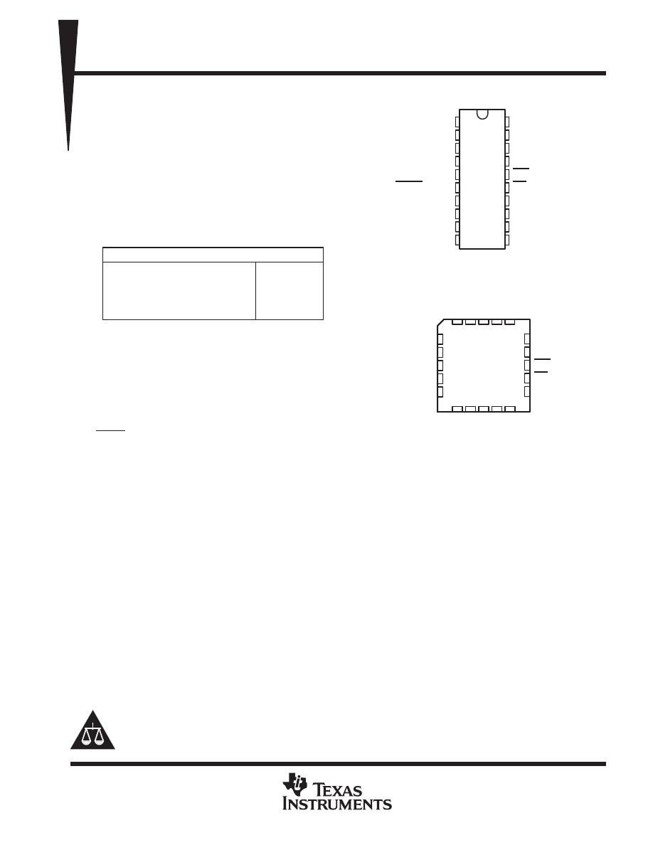
DW, N OR PW PACKAGE
(TOP VIEW)
3
2
1 20 19
9 10 11 12 13
4
5
6
7
8
18
17
16
15
14
REFB
V
DD
WR
CS
DB0 (LSB)
REFA
DGND
DACA/DACB
(MSB) DB7
DB6
FN PACKAGE
(TOP VIEW)
RFBA
OUT
A
AGND
D
B2
D
B1
OUTB
RFBB
D
B5
D
B4
D
B3
SLAS062D − JANUARY 1987 − REVISED JUNE 2007
2
POST OFFICE BOX 655303
•
DALLAS, TEXAS 75265
functional block diagram
ÎÎÎÎÎ
ÎÎÎÎÎ
ÎÎÎÎÎ
ÎÎÎÎÎ
ÎÎÎ
ÎÎÎ
ÎÎÎ
ÎÎÎ
ÎÎÎÎÎ
ÎÎÎÎÎ
ÎÎÎÎÎ
ÎÎÎÎÎ
ÎÎÎ
ÎÎÎ
ÎÎÎ
ÎÎÎ
8
8
8
8
DACA/DACB
REFB
18
OUTB
20
RFBB
19
AGND
1
OUTA
2
RFBA
3
REFA
4
Input
Buffer
Logic
Control
DB0
DB7
CS
WR
15
16
6
Data
Inputs
7
8
9
10
11
12
13
14
DACA
DACB
Latch B
Latch A
operating sequence
th(DAC)
th(CS)
tsu(CS)
tsu(DAC)
tw(WR)
th(D)
tsu(D)
Data In Stable
DB0 − DB7
WR
CS
DACA/DACB
SLAS062D − JANUARY 1987 − REVISED JUNE 2007
3
POST OFFICE BOX 655303
•
DALLAS, TEXAS 75265
absolute maximum ratings over operating free-air temperature range (unless otherwise noted)
†
Supply voltage range, V
DD
(to AGND or DGND)
−0.3V to 16.5V
. . . . . . . . . . . . . . . . . . . . . . . . . . . . . . . . . . . . . .
Voltage between AGND and DGND
±
V
DD
. . . . . . . . . . . . . . . . . . . . . . . . . . . . . . . . . . . . . . . . . . . . . . . . . . . . . . . . .
Input voltage range, V
I
(to DGND)
−0.3V to V
DD
+ 0.3
. . . . . . . . . . . . . . . . . . . . . . . . . . . . . . . . . . . . . . . . . . . . . . .
Reference voltage, V
refA
or V
refB
(to AGND)
±
25V
. . . . . . . . . . . . . . . . . . . . . . . . . . . . . . . . . . . . . . . . . . . . . . . . .
Feedback voltage V
RFBA
or V
RFBB
(to AGND)
±
25V
. . . . . . . . . . . . . . . . . . . . . . . . . . . . . . . . . . . . . . . . . . . . . . .
Input voltage (voltage mode out A, out B to AGND)
−0.3V to V
DD
+ 0.3
. . . . . . . . . . . . . . . . . . . . . . . . . . . . . . . .
Output voltage, V
OA
or V
OB
(to AGND)
±
25V
. . . . . . . . . . . . . . . . . . . . . . . . . . . . . . . . . . . . . . . . . . . . . . . . . . . . . .
Peak input current
10
µ
A
. . . . . . . . . . . . . . . . . . . . . . . . . . . . . . . . . . . . . . . . . . . . . . . . . . . . . . . . . . . . . . . . . . . . . . . .
Operating free-air temperature range, T
A
: TLC7528C
0
°
C to +70
°
C
. . . . . . . . . . . . . . . . . . . . . . . . . . . . . . . . . .
TLC7528I
−25
°
C to +85
°
C
. . . . . . . . . . . . . . . . . . . . . . . . . . . . . . .
TLC7528E
−40
°
C to +85
°
C
. . . . . . . . . . . . . . . . . . . . . . . . . . . . . . .
Storage temperature range, T
stg
−65
°
C to +150
°
C
. . . . . . . . . . . . . . . . . . . . . . . . . . . . . . . . . . . . . . . . . . . . . . . . .
Case temperature for 10 seconds, T
C
: FN package
+260
°
C
. . . . . . . . . . . . . . . . . . . . . . . . . . . . . . . . . . . . . . . . .
Lead temperature 1,6mm (1/16 inch) from case for 10 seconds: DW or N package
+260
°
C
. . . . . . . . . . . . . .
† Stresses beyond those listed under “absolute maximum ratings” may cause permanent damage to the device. These are stress ratings only, and
functional operation of the device at these or any other conditions beyond those indicated under “recommended operating conditions” is not
implied. Exposure to absolute-maximum-rated conditions for extended periods may affect device reliability.
package/ordering information
For the most current package and ordering information, see the Package Option Addendum at the end of this
document, or see the TI website at www.ti.com.
recommended operating conditions
VDD = 4.75V to 5.25V
VDD = 14.5V to 15.5V
UNIT
MIN
NOM
MAX
MIN
NOM
MAX
UNIT
Reference voltage, VrefA or VrefB
±
10
±
10
V
High-level input voltage, VIH
2.4
13.5
V
Low-level input voltage, VIL
0.8
1.5
V
CS setup time, tsu(CS)
50
50
ns
CS hold time, th(CS)
0
0
ns
DAC select setup time, tsu(DAC)
50
50
ns
DAC select hold time, th(DAC)
10
10
ns
Data bus input setup time tsu(D)
25
25
ns
Data bus input hold time th(D)
10
10
ns
Pulse duration, WR low, tw(WR)
50
50
ns
TLC7628C
0
+70
0
+70
Operating free-air temperature, TA
TLC7628I
− 25
+85
− 25
+85
°
C
Operating free-air temperature, TA
TLC7628E
− 40
+85
− 40
+85
C
SLAS062D − JANUARY 1987 − REVISED JUNE 2007
4
POST OFFICE BOX 655303
•
DALLAS, TEXAS 75265
electrical characteristics over recommended operating free-air temperature range,
V
refA
= V
refB
= 10V, V
OA
and V
OB
at 0V (unless otherwise noted)
PARAMETER
TEST CONDITIONS
VDD = 5V
VDD = 15V
UNIT
PARAMETER
TEST CONDITIONS
MIN
TYP†
MAX
MIN
TYP†
MAX
UNIT
IIH
High-level input current
VI = VDD
10
10
µ
A
IIL
Low-level input current
VI = 0
5
12
− 10
5
12
− 10
µ
A
Reference input impedance
REFA or REFB to AGND
20
20
k
Ω
IIkg
Output leakage current
OUTA
DAC data latch loaded with
00000000, VrefA =
±
10V
±
400
±
200
nA
IIkg
Output leakage current
OUTB
DAC data latch loaded with
00000000, VrefB =
±
10V
±
400
±
200
nA
Input resistance match
(REFA to REFB)
±
1%
±
1%
DC supply sensitivity,
∆
gain/
∆
VDD
∆
VDD =
±
10%
0.04
0.02
%/%
IDD
Supply current (quiescent)
All digital inputs at VIHmin or
VILmax
2
2
mA
IDD
Supply current (standby)
All digital inputs at 0V or VDD
0.5
0.5
mA
DB0−DB7
10
10
pF
Ci
Input capacitance
WR, CS,
DACA/DACB
15
15
pF
Co
Output capacitance (OUTA, OUTB)
DAC data latches loaded with
00000000
50
50
pF
Co
Output capacitance (OUTA, OUTB)
DAC data latches loaded with
11111111
120
120
pF
† All typical values are at TA = +25
°
C.
SLAS062D − JANUARY 1987 − REVISED JUNE 2007
5
POST OFFICE BOX 655303
•
DALLAS, TEXAS 75265
operating characteristics over recommended operating free-air temperature range,
V
refA
= V
refB
= 10V, V
OA
and V
OB
at 0V (unless otherwise noted)
PARAMETER
TEST CONDITIONS
VDD = 5V
VDD = 15V
UNIT
PARAMETER
TEST CONDITIONS
MIN
TYP
MAX
MIN
TYP
MAX
UNIT
Linearity error
±
1/2
±
1/2
LSB
Settling time (to 1/2LSB)
See Note 1
100
100
ns
Gain error
See Note 2
2.5
2.5
LSB
AC feedthrough
REFA to OUTA
See Note 3
− 65
− 65
dB
AC feedthrough
REFB to OUTB
See Note 3
− 65
− 65
dB
Temperature coefficient of gain
See Note 4
0.007
0.0035
%FSR/
°
C
Propagation delay (from digital input to
90% of final analog output current)
See Note 5
80
80
ns
Channel-to-channel
REFA to OUTB
See Note 6
77
77
dB
Channel-to-channel
isolation
REFB to OUTA
See Note 7
77
77
dB
Digital-to-analog glitch impulse area
Measured for code transition from
00000000 to 11111111,
TA = +25
°
C
160
440
nV−s
Digital crosstalk
Measured for code transition from
00000000 to 11111111,
TA = +25
°
C
30
60
nV−s
Harmonic distortion
Vi = 6V,
f = 1kHz,
TA = +25
°
C
− 85
− 85
dB
NOTES:
1. OUTA, OUTB load = 100
Ω
, Cext = 13pF; WR and CS at 0V; DB0−DB7 at 0V to VDD or VDD to 0V.
2. Gain error is measured using an internal feedback resistor. Nominal full scale range (FSR) = Vref − 1LSB.
3. Vref = 20V peak-to-peak, 100kHz sine wave; DAC data latches loaded with 00000000.
4. Temperature coefficient of gain measured from 0
°
C to +25
°
C or from +25
°
C to +70
°
C.
5. VrefA = VrefB = 10V; OUTA/OUTB load = 100
Ω
, Cext = 13pF; WR and CS at 0V; DB0−DB7 at 0V to VDD or VDD to 0V.
6. Both DAC latches loaded with 11111111; VrefA = 20V peak-to-peak, 100kHz sine wave; VrefB = 0; TA = +25
°
C.
7. Both DAC latches loaded with 11111111; VrefB = 20V peak-to-peak, 100kHz sine wave; VrefA = 0; TA = +25
°
C.
PRINCIPLES OF OPERATION
These devices contain two identical, 8-bit-multiplying D/A converters, DACA and DACB. Each DAC consists
of an inverted R-2R ladder, analog switches, and input data latches. Binary-weighted currents are switched
between DAC output and AGND, thus maintaining a constant current in each ladder leg independent of the
switch state. Most applications require only the addition of an external operational amplifier and voltage
reference. A simplified D/A circuit for DACA with all digital inputs low is shown in Figure 1.
Figure 2 shows the DACA equivalent circuit. A similar equivalent circuit can be drawn for DACB. Both DACs
share the analog ground terminal 1 (AGND). With all digital inputs high, the entire reference current flows to
OUTA. A small leakage current (I
Ikg
) flows across internal junctions, and as with most semiconductor devices,
doubles every 10
°
C. C
o
is due to the parallel combination of the NMOS switches and has a value that depends
on the number of switches connected to the output. The range of C
o
is 50pF to 120pF maximum. The equivalent
output resistance (r
o
) varies with the input code from 0.8R to 3R where R is the nominal value of the ladder
resistor in the R-2R network.
These devices interface to a microprocessor through the data bus, CS, WR, and DACA/DACB control signals.
When CS and WR are both low, the TLC7528 analog output, specified by the DACA/DACB control line,
responds to the activity on the DB0−DB7 data bus inputs. In this mode, the input latches are transparent and
input data directly affects the analog output. When either the CS signal or WR signal goes high, the data on the
DB0−DB7 inputs is latched until the CS and WR signals go low again. When CS is high, the data inputs are
disabled regardless of the state of the WR signal.
SLAS062D − JANUARY 1987 − REVISED JUNE 2007
6
POST OFFICE BOX 655303
•
DALLAS, TEXAS 75265
PRINCIPLES OF OPERATION
The digital inputs of these devices provide TTL compatibility when operated from a supply voltage of 5V. These
devices can operate with any supply voltage in the range from 5V to 15V; however, input logic levels are not
TTL compatible above 5V.
DACA Data Latches and Drivers
REFA
AGND
OUTA
RFBA
RFB
R
R
R
2R
2R
S8
2R
S3
2R
S2
S1
2R
Figure 1. Simplified Functional Circuit for DACA
R
I
256
OUTA
RFBA
RFB
COUT
IIkg
AGND
REFA
Figure 2. TLC7528 Equivalent Circuit, DACA Latch Loaded With 11111111
MODE SELECTION TABLE
DACA/DACB
CS
WR
DACA
DACB
L
H
X
X
L
L
H
X
L
L
X
H
Write
Hold
Hold
Hold
Hold
Write
Hold
Hold
L = low level, H = high level, X = don’t care
SLAS062D − JANUARY 1987 − REVISED JUNE 2007
7
POST OFFICE BOX 655303
•
DALLAS, TEXAS 75265
APPLICATION INFORMATION
These devices are capable of performing 2-quadrant or full 4-quadrant multiplication. Circuit configurations for
2-quadrant and 4-quadrant multiplication are shown in Figures 3 and 4. Tables 1 and 2 summarize input coding
for unipolar and bipolar operation.
ÎÎÎ
ÎÎÎ
ÎÎÎ
ÎÎÎ
ÎÎÎÎ
ÎÎÎÎ
ÎÎÎÎ
ÎÎÎÎ
ÎÎÎÎ
ÎÎÎÎ
ÎÎÎÎ
DGND
VOB
VOA
VI(B)
±
10 V
R3 (see Note A)
R1 (see Note A)
AGND
+
−
C1
(see Note B)
C2
(see Note B)
R2 (see Note A)
R4 (see Note A)
+
−
AGND
OUTB
RFBB
AGND
OUTA
5
VDD
17
7
14
DACA / DACB
DB0
DB7
Input
Buffer
8
8
8
8
REFB
RFBA
REFA
Latch
Control
Logic
CS
WR
16
15
6
RECOMMENDED TRIM
RESISTOR VALUES
R1, R3
R2, R4
500
Ω
150
Ω
DACA
DACB
Latch
VI(A)
±
10 V
NOTES: A. R1, R2, R3, and R4 are used only if gain adjustment is required. See table for recommended values. Make gain adjustment with
digital input of 255.
B. C1 and C2 phase compensation capacitors (10pF to 15pF) are required when using high-speed amplifiers to prevent ringing or
oscillation.
Figure 3. Unipolar Operation (2-Quadrant Multiplication)
SLAS062D − JANUARY 1987 − REVISED JUNE 2007
8
POST OFFICE BOX 655303
•
DALLAS, TEXAS 75265
APPLICATION INFORMATION
ÎÎÎ
ÎÎÎ
ÎÎÎ
ÎÎÎ
ÎÎÎÎ
ÎÎÎÎ
ÎÎÎÎ
ÎÎÎÎ
ÎÎÎÎ
ÎÎÎÎ
ÎÎÎÎ
+
−
R11
5 k
Ω
A2
VOA
DACB
R6
20 k
Ω
(see Note B)
VOB
+
−
AGND
A1
DGND
A4
R3
(see Note A)
R1
(see Note A)
AGND
+
−
C1
(see Note C)
C2
(see Note C)
R2 (see Note A)
R4 (see Note A)
+
−
AGND
OUTB
RFBB
AGND
OUTA
5
VDD
17
7
14
DACA/
DACB
DB0
DB7
8
8
8
8
REFB
RFBA
DACA
CS
WR
16
15
6
A3
R10
20 k
Ω
(see Note B)
Latch
Input
Buffer
Control
Logic
Latch
R8
20 k
Ω
R7
10 k
Ω
(see Note B)
R9
10 k
Ω
(see Note B)
R11
5 k
Ω
R5
20 k
Ω
VI(A)
±
10 V
VI(B)
±
10 V
NOTES: A. R1, R2, R3, and R4 are used only if gain adjustment is required. See table in Figure 3 for recommended values. Adjust R1 for
VOA = 0V with code 10000000 in DACA latch. Adjust R3 for VOB = 0V with 10000000 in DACB latch.
B. Matching and tracking are essential for resistor pairs R6, R7, R9, and R10.
C. C1 and C2 phase compensation capacitors (10pF to 15pF) may be required if A1 and A3 are high-speed amplifiers.
Figure 4. Bipolar Operation (4-Quadrant Operation)
Table 1. Unipolar Binary Code
Table 2. Bipolar (Offset Binary) Code
DAC LATCH CONTENTS
ANALOG OUTPUT
DAC LATCH CONTENTS
ANALOG OUTPUT
MSB
LSB†
ANALOG OUTPUT
MSB
LSB‡
ANALOG OUTPUT
1 1 1 1 1 1 1 1
1 0 0 0 0 0 0 1
1 0 0 0 0 0 0 0
0 1 1 1 1 1 1 1
0 0 0 0 0 0 0 1
0 0 0 0 0 0 0 0
−VI (255/256)
−VI (129/256)
−VI (128/256) = − Vi/2
− VI (127/256)
− VI (1/256)
− VI (0/256) = 0
1 1 1 1 1 1 1 1
1 0 0 0 0 0 0 1
1 0 0 0 0 0 0 0
0 1 1 1 1 1 1 1
0 0 0 0 0 0 0 1
0 0 0 0 0 0 0 0
VI (127/128)
VI (1/128)
0V
− VI (1/128)
− VI (127/128)
− VI (128/128)
† 1LSB = (2−8)VI
‡ 1LSB = (2−7)VI
SLAS062D − JANUARY 1987 − REVISED JUNE 2007
9
POST OFFICE BOX 655303
•
DALLAS, TEXAS 75265
APPLICATION INFORMATION
microprocessor interface information
A + 1
A
A8 − A15
CPU
8051
WR
ALE
TLC7528
DACA/DACB
CS
WR
DB0
DB7
AD0 − AD7
Data Bus
Address Bus
Latch
Address
Decode
Logic
NOTE A: A = decoded address for TLC7528 DACA
A + 1 = decoded address for TLC7528 DACB
8
8
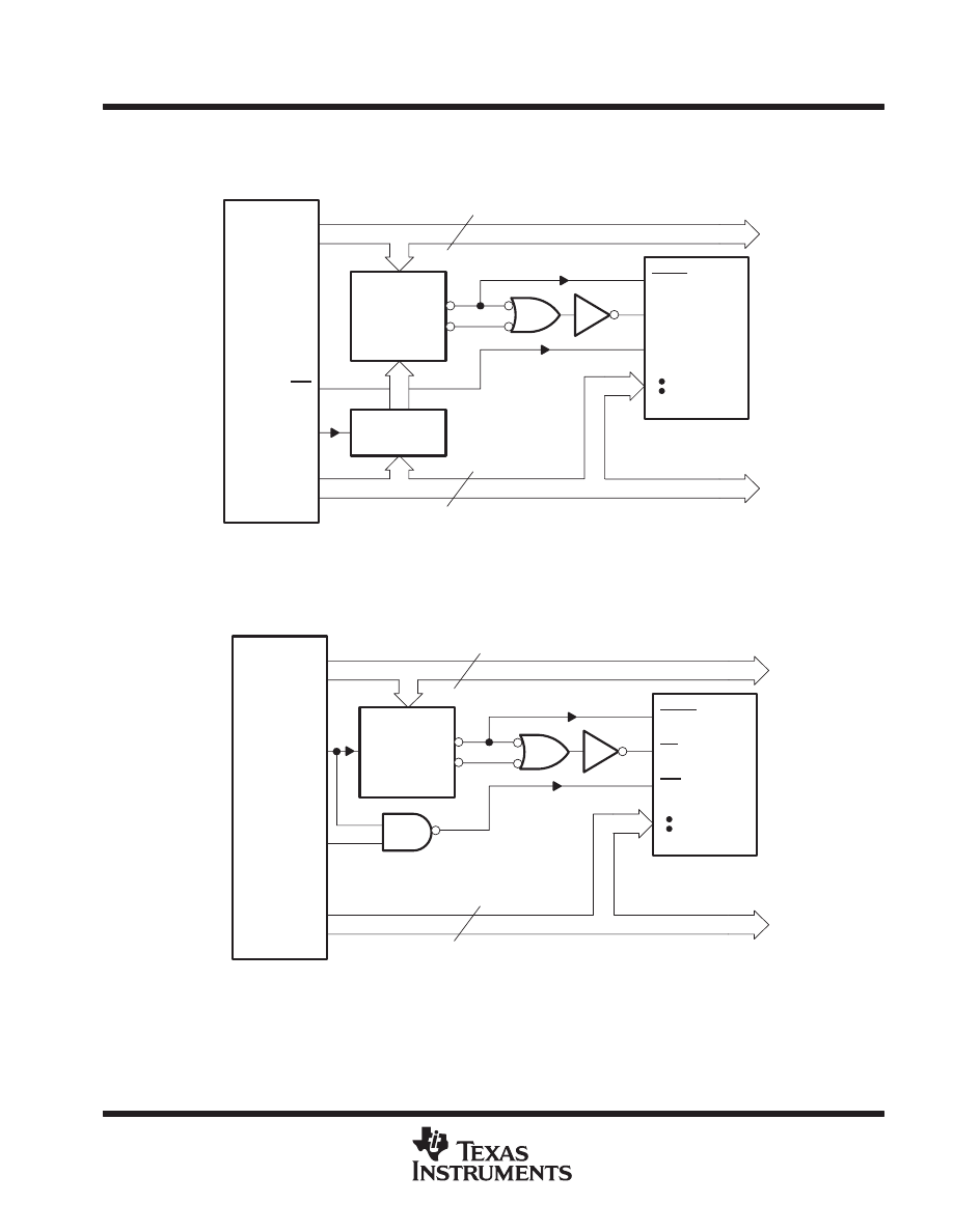
Figure 5. TLC7528: Intel 8051 Interface
φ
2
Address
Decode
Logic
Address Bus
Data Bus
AD0 − AD7
DB7
DB0
WR
CS
DACA/DACB
TLC7528
VMA
CPU
6800
A8 − A15
A
A + 1
NOTE A: A = decoded address for TLC7528 DACA
A + 1 = decoded address for TLC7528 DACB
8
8
Figure 6. TLC7528: 6800 Interface
SLAS062D − JANUARY 1987 − REVISED JUNE 2007
10
POST OFFICE BOX 655303
•
DALLAS, TEXAS 75265
APPLICATION INFORMATION
WR
Address
Decode
Logic
Address Bus
Data Bus
D0 − D7
DB7
DB0
WR
CS
DACA/DACB
TLC7528
IORQ
CPU
Z80-A
A8 − A15
A
A + 1
NOTE A: A = decoded address for TLC7528 DACA
A + 1 = decoded address for TLC7528 DACB
8
8
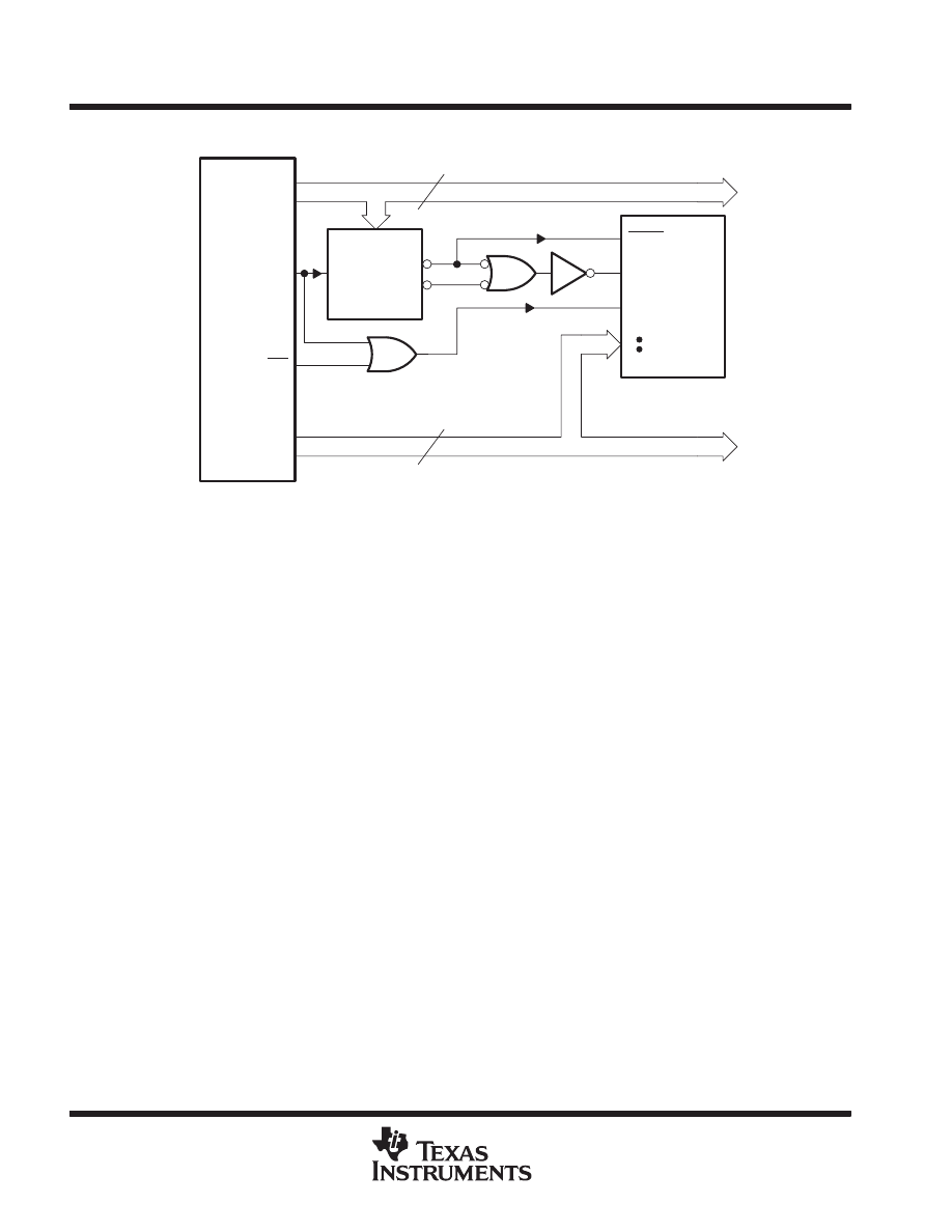
Figure 7. TLC7528 To Z-80A Interface
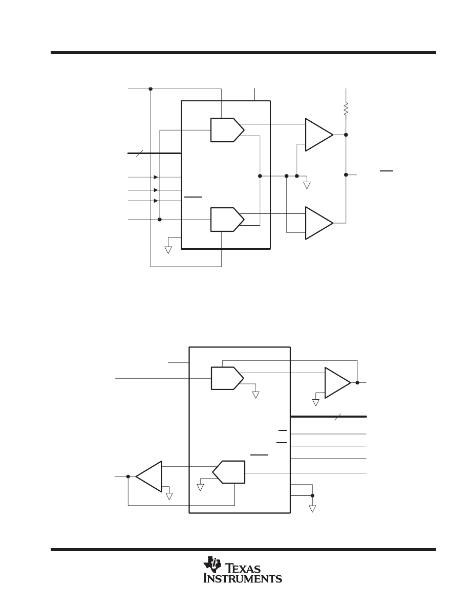
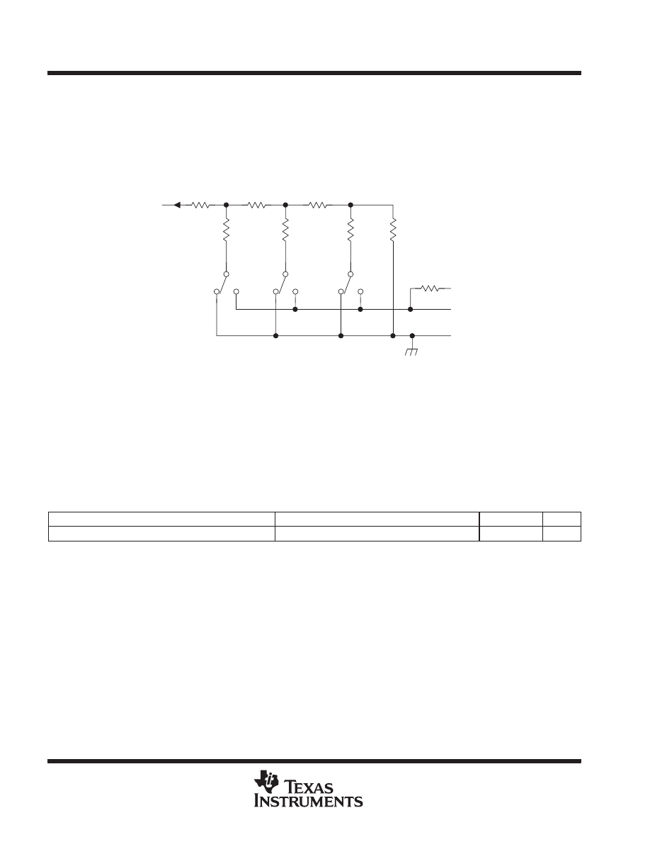
programmable window detector
The programmable window comparator shown in Figure 8 determines if voltage applied to the DAC feedback
resistors are within the limits programmed into the data latches of these devices. Input signal range depends
on the reference and polarity, that is, the test input range is 0 to −V
ref
. The DACA and DACB data latches are
programmed with the upper and lower test limits. A signal within the programmed limits drives the output high.
SLAS062D − JANUARY 1987 − REVISED JUNE 2007
11
POST OFFICE BOX 655303
•
DALLAS, TEXAS 75265
APPLICATION INFORMATION
REFB
19
RFBB
OUTB
AGND
TLC7528
REFA
DB0 − DB7
CS
WR
DACA / DACB
DGND
Vref
Data Inputs
4
5
18
6
16
15
14 − 7
Test Input
0 to −Vref
RFBA
3
VDD
17
OUTA
2
1
20
PASS / FAIL Output
1 k
Ω
VCC
+
−
+
−
DACB
DACA
8
Figure 8. Digitally-Programmable Window Comparator (Upper- and Lower-Limit Tester)
digitally controlled signal attenuator
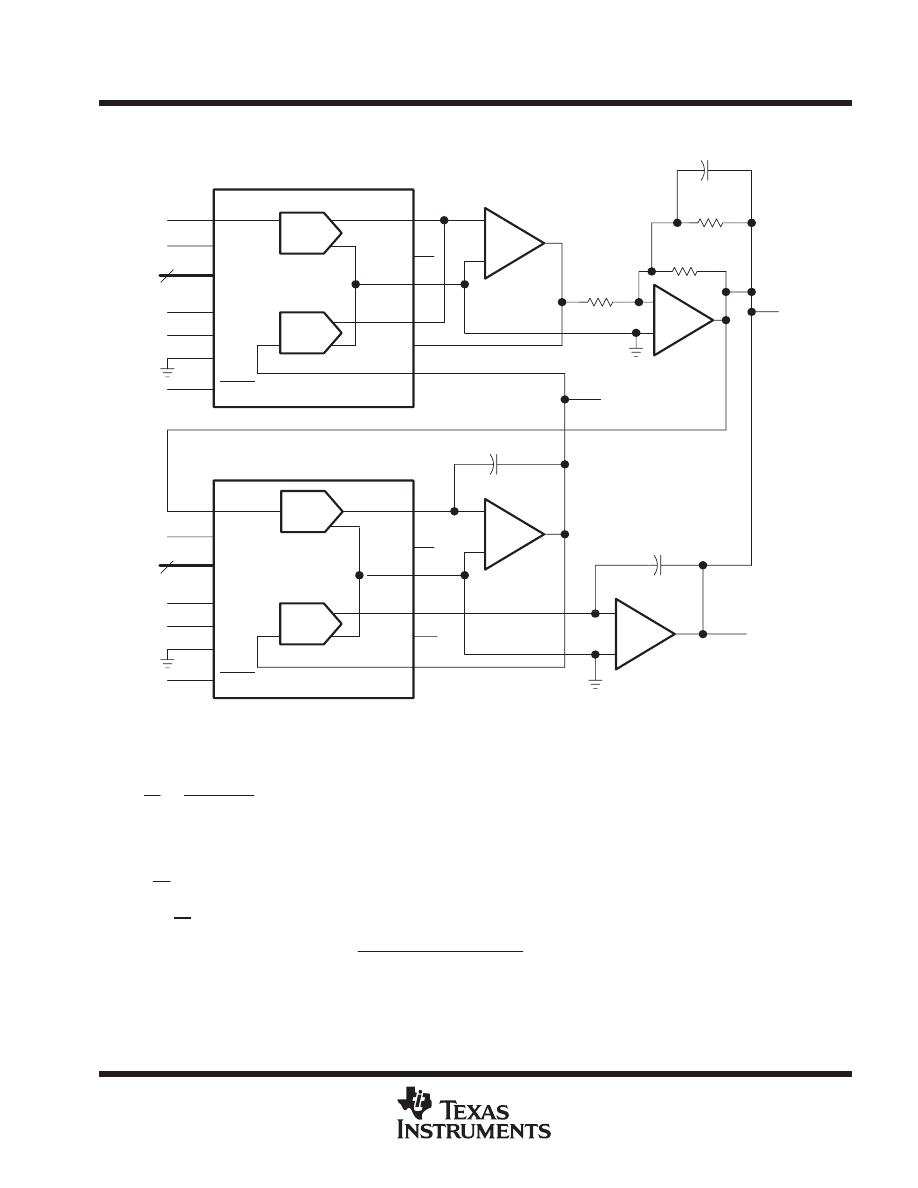
Figure 9 shows a TLC7528 configured as a two-channel programmable attenuator. Applications include stereo
audio and telephone signal level control. Table 3 shows input codes vs attenuation for a 0 to 15.5dB range.
Output
A1
A2
VOB
VDD
TLC7528
DGND
AGND
REFB
DACA / DACB
WR
CS
DB0 − DB7
OUTA
RFBA
REFA
RFBB
OUTB
Data Bus
3
2
15
16
6
18
1
5
19
17
4
20
DACA
DACB
Attenuation dB = − 20 log10 D/256, D = digital input code
8
14 − 7
VIA
Figure 9. Digitally Controlled Dual Telephone Attenuator
SLAS062D − JANUARY 1987 − REVISED JUNE 2007
12
POST OFFICE BOX 655303
•
DALLAS, TEXAS 75265
APPLICATION INFORMATION
Table 3. Attenuation vs DACA, DACB Code
ATTN (dB)
DAC INPUT CODE
CODE IN
DECIMAL
ATTN (dB)
DAC INPUT CODE
CODE IN
DECIMAL
0
1 1 1 1 1 1 1 1
255
8.0
0 1 1 0 0 1 1 0
102
0.5
1 1 1 1 0 0 1 0
242
8.5
0 1 1 0 0 0 0 0
96
1.0
1 1 1 0 0 1 0 0
228
9.0
0 1 0 1 1 0 1 1
91
1.5
1 1 0 1 0 1 1 1
215
9.5
0 1 0 1 0 1 1 0
86
2.0
1 1 0 0 1 0 1 1
203
10.0
0 1 0 1 0 0 0 1
81
2.5
1 1 0 0 0 0 0 0
192
10.5
0 1 0 0 1 1 0 0
76
3.0
1 0 1 1 0 1 0 1
181
11.0
0 1 0 0 1 0 0 0
72
3.5
1 0 1 0 1 0 1 1
171
11.5
0 1 0 0 0 1 0 0
68
4.0
1 0 1 0 0 0 1 0
162
12.0
0 1 0 0 0 0 0 0
64
4.5
1 0 0 1 1 0 0 0
152
12.5
0 0 1 1 1 1 0 1
61
5.0
1 0 0 1 1 1 1 1
144
13.0
0 0 1 1 1 0 0 1
57
5.5
1 0 0 0 1 0 0 0
136
13.5
0 0 1 1 0 1 1 0
54
6.0
1 0 0 0 0 0 0 0
128
14.0
0 0 1 1 0 0 1 1
51
6.5
0 1 1 1 1 0 0 1
121
14.5
0 0 1 1 0 0 0 0
48
7.0
0 1 1 1 0 0 1 0
114
15.0
0 0 1 0 1 1 1 0
46
7.5
0 1 1 0 1 1 0 0
108
15.5
0 0 1 0 1 0 1 1
43
programmable state-variable filter
This programmable state-variable or universal filter configuration provides low-pass, high-pass, and bandpass
outputs, and is suitable for applications requiring microprocessor control of filter parameters.
As shown in Figure 10, DACA1 and DACB1 control the gain and Q of the filter while DACA2 and DACB2 control
the cutoff frequency. Both halves of the DACA2 and DACB2 must track accurately in order for the
cutoff-frequency equation to be true. With the TLC7528, this is easy to achieve.
fc
+
1
2
p
R1C1
The programmable range for the cutoff or center frequency is 0 to 15kHz with a Q ranging from 0.3 to 4.5. This
defines the limits of the component values.
256
(DAC ladder resistance)
DAC digital code
SLAS062D − JANUARY 1987 − REVISED JUNE 2007
13
POST OFFICE BOX 655303
•
DALLAS, TEXAS 75265
APPLICATION INFORMATION
Bandpass Out
High Pass
Out
30 k
Ω
47 pF
C3
R5
R4
R3
Low Pass Out
1000 pF
C2
C1
1000 pF
+
−
DACA
(R1)
(R2)
DACB
TLC7528
+
−
OUTA
RFBA
AGND
OUTB
REFB
RFBB
2
3
1
20
19
18
REFA
VDD
CS
WR
DGND
DACA / DACB
DACA2 and DACB2
A3
+
−
A2
A1
DACA1 AND DACB1
Data In
VI
DACA / DACB
6
DGND
5
WR
16
CS
15
DB0 − DB7
14 − 7
17
VDD
REFA
4
18
19
20
1
3
2
RFBB
REFB
OUTB
AGND
RFBA
OUTA
+
−
TLC7528
DACB
(RF)
(RS)
DACA
Q
+
R
3
R
4
R
F
R
fb(DACB1)
C1 = C2, R1 = R2, R4 = R5
G
+
–
R
F
R
S
30 k
Ω
10 k
Ω
A4
14 − 7
DB0 − DB7
8
8
Data In
6
5
16
15
17
4
R
fb
is the internal resistor connected between OUTB and RFBB
Where:
Circuit Equations:
NOTES: A. Op-amps A1, A2, A3, and A4 are TL287.
B. CS compensates for the op-amp gain-bandwidth limitations.
C. DAC equivalent resistance equals
Figure 10. Digitally Controlled State-Variable Filter
SLAS062D − JANUARY 1987 − REVISED JUNE 2007
14
POST OFFICE BOX 655303
•
DALLAS, TEXAS 75265
APPLICATION INFORMATION
voltage-mode operation
It is possible to operate the current multiplying D/A converter of these devices in a voltage mode. In the voltage
mode, a fixed voltage is placed on the current output terminal. The analog output voltage is then available at
the reference voltage terminal. Figure 11 is an example of a current multiplying D/A, that operates in the voltage
mode.
2R
2R
2R
“0”
“1”
2R
R
R
R
R
Out (Fixed Input Voltage)
AGND
REF
(Analog Output Voltage)
Figure 11. Voltage-Mode Operation
The following equation shows the relationship between the fixed input voltage and the analog output voltage:
V
O
= V
I
(D/256)
Where:
V
O
= analog output voltage
V
I
= fixed input voltage (must not be forced below 0V.)
D = digital input code converted to decimal
In voltage-mode operation, these devices meet the following specification:
PARAMETER
TEST CONDITIONS
MIN
MAX
UNIT
Linearity error at REFA or REFB
VDD = 5V,
OUTA or OUTB at 2.5V,
TA = +25
°
C
1
LSB

Revision History
DATE
REV
PAGE
SECTION
DESCRIPTION
6/07
D
Front Page
—
Deleted Available Options table.
6/07
D
3
—
Inserted Package/Ordering information.
NOTE: Page numbers for previous revisions may differ from page numbers in the current version.
PACKAGING INFORMATION
Orderable Device
Status
(1)
Package
Type
Package
Drawing
Pins Package
Qty
Eco Plan
(2)
Lead/Ball Finish
MSL Peak Temp
(3)
TLC7528CDW
ACTIVE
SOIC
DW
20
25
Green (RoHS &
no Sb/Br)
CU NIPDAU
Level-1-260C-UNLIM
TLC7528CDWG4
ACTIVE
SOIC
DW
20
25
Green (RoHS &
no Sb/Br)
CU NIPDAU
Level-1-260C-UNLIM
TLC7528CDWR
ACTIVE
SOIC
DW
20
2000 Green (RoHS &
no Sb/Br)
CU NIPDAU
Level-1-260C-UNLIM
TLC7528CDWRG4
ACTIVE
SOIC
DW
20
2000 Green (RoHS &
no Sb/Br)
CU NIPDAU
Level-1-260C-UNLIM
TLC7528CFN
ACTIVE
PLCC
FN
20
46
Green (RoHS &
no Sb/Br)
CU SN
Level-1-260C-UNLIM
TLC7528CFNG3
ACTIVE
PLCC
FN
20
46
Green (RoHS &
no Sb/Br)
CU SN
Level-1-260C-UNLIM
TLC7528CFNR
ACTIVE
PLCC
FN
20
1000 Green (RoHS &
no Sb/Br)
CU SN
Level-1-260C-UNLIM
TLC7528CFNRG3
ACTIVE
PLCC
FN
20
1000 Green (RoHS &
no Sb/Br)
CU SN
Level-1-260C-UNLIM
TLC7528CN
ACTIVE
PDIP
N
20
20
Pb-Free
(RoHS)
CU NIPDAU
N / A for Pkg Type
TLC7528CNE4
ACTIVE
PDIP
N
20
20
Pb-Free
(RoHS)
CU NIPDAU
N / A for Pkg Type
TLC7528CNS
ACTIVE
SO
NS
20
40
Green (RoHS &
no Sb/Br)
CU NIPDAU
Level-1-260C-UNLIM
TLC7528CNSG4
ACTIVE
SO
NS
20
40
Green (RoHS &
no Sb/Br)
CU NIPDAU
Level-1-260C-UNLIM
TLC7528CNSR
ACTIVE
SO
NS
20
2000 Green (RoHS &
no Sb/Br)
CU NIPDAU
Level-1-260C-UNLIM
TLC7528CNSRG4
ACTIVE
SO
NS
20
2000 Green (RoHS &
no Sb/Br)
CU NIPDAU
Level-1-260C-UNLIM
TLC7528CPW
ACTIVE
TSSOP
PW
20
70
Green (RoHS &
no Sb/Br)
CU NIPDAU
Level-1-260C-UNLIM
TLC7528CPWG4
ACTIVE
TSSOP
PW
20
70
Green (RoHS &
no Sb/Br)
CU NIPDAU
Level-1-260C-UNLIM
TLC7528CPWR
ACTIVE
TSSOP
PW
20
2000 Green (RoHS &
no Sb/Br)
CU NIPDAU
Level-1-260C-UNLIM
TLC7528CPWRG4
ACTIVE
TSSOP
PW
20
2000 Green (RoHS &
no Sb/Br)
CU NIPDAU
Level-1-260C-UNLIM
TLC7528EDW
ACTIVE
SOIC
DW
20
25
Green (RoHS &
no Sb/Br)
CU NIPDAU
Level-1-260C-UNLIM
TLC7528EDWG4
ACTIVE
SOIC
DW
20
25
Green (RoHS &
no Sb/Br)
CU NIPDAU
Level-1-260C-UNLIM
TLC7528EDWR
ACTIVE
SOIC
DW
20
2000 Green (RoHS &
no Sb/Br)
CU NIPDAU
Level-1-260C-UNLIM
TLC7528EDWRG4
ACTIVE
SOIC
DW
20
2000 Green (RoHS &
no Sb/Br)
CU NIPDAU
Level-1-260C-UNLIM
TLC7528EN
ACTIVE
PDIP
N
20
20
Pb-Free
(RoHS)
CU NIPDAU
N / A for Pkg Type
TLC7528ENE4
ACTIVE
PDIP
N
20
20
Pb-Free
(RoHS)
CU NIPDAU
N / A for Pkg Type
TLC7528IDW
ACTIVE
SOIC
DW
20
25
Green (RoHS &
no Sb/Br)
CU NIPDAU
Level-1-260C-UNLIM
PACKAGE OPTION ADDENDUM
www.ti.com
30-May-2007
Addendum-Page 1
Orderable Device
Status
(1)
Package
Type
Package
Drawing
Pins Package
Qty
Eco Plan
(2)
Lead/Ball Finish
MSL Peak Temp
(3)
TLC7528IDWG4
ACTIVE
SOIC
DW
20
25
Green (RoHS &
no Sb/Br)
CU NIPDAU
Level-1-260C-UNLIM
TLC7528IDWR
ACTIVE
SOIC
DW
20
2000 Green (RoHS &
no Sb/Br)
CU NIPDAU
Level-1-260C-UNLIM
TLC7528IDWRG4
ACTIVE
SOIC
DW
20
2000 Green (RoHS &
no Sb/Br)
CU NIPDAU
Level-1-260C-UNLIM
TLC7528IFN
ACTIVE
PLCC
FN
20
46
Green (RoHS &
no Sb/Br)
CU SN
Level-1-260C-UNLIM
TLC7528IFNG3
ACTIVE
PLCC
FN
20
46
Green (RoHS &
no Sb/Br)
CU SN
Level-1-260C-UNLIM
TLC7528IFNR
ACTIVE
PLCC
FN
20
1000 Green (RoHS &
no Sb/Br)
CU SN
Level-1-260C-UNLIM
TLC7528IFNRG3
ACTIVE
PLCC
FN
20
1000 Green (RoHS &
no Sb/Br)
CU SN
Level-1-260C-UNLIM
TLC7528IN
ACTIVE
PDIP
N
20
20
Pb-Free
(RoHS)
CU NIPDAU
N / A for Pkg Type
TLC7528INE4
ACTIVE
PDIP
N
20
20
Pb-Free
(RoHS)
CU NIPDAU
N / A for Pkg Type
TLC7528IPW
ACTIVE
TSSOP
PW
20
70
Green (RoHS &
no Sb/Br)
CU NIPDAU
Level-1-260C-UNLIM
TLC7528IPWG4
ACTIVE
TSSOP
PW
20
70
Green (RoHS &
no Sb/Br)
CU NIPDAU
Level-1-260C-UNLIM
TLC7528IPWR
ACTIVE
TSSOP
PW
20
2000 Green (RoHS &
no Sb/Br)
CU NIPDAU
Level-1-260C-UNLIM
TLC7528IPWRG4
ACTIVE
TSSOP
PW
20
2000 Green (RoHS &
no Sb/Br)
CU NIPDAU
Level-1-260C-UNLIM
(1)
The marketing status values are defined as follows:
ACTIVE: Product device recommended for new designs.
LIFEBUY: TI has announced that the device will be discontinued, and a lifetime-buy period is in effect.
NRND: Not recommended for new designs. Device is in production to support existing customers, but TI does not recommend using this part in
a new design.
PREVIEW: Device has been announced but is not in production. Samples may or may not be available.
OBSOLETE: TI has discontinued the production of the device.
(2)
Eco Plan - The planned eco-friendly classification: Pb-Free (RoHS), Pb-Free (RoHS Exempt), or Green (RoHS & no Sb/Br) - please check
http://www.ti.com/productcontent
for the latest availability information and additional product content details.
TBD: The Pb-Free/Green conversion plan has not been defined.
Pb-Free (RoHS): TI's terms "Lead-Free" or "Pb-Free" mean semiconductor products that are compatible with the current RoHS requirements
for all 6 substances, including the requirement that lead not exceed 0.1% by weight in homogeneous materials. Where designed to be soldered
at high temperatures, TI Pb-Free products are suitable for use in specified lead-free processes.
Pb-Free (RoHS Exempt): This component has a RoHS exemption for either 1) lead-based flip-chip solder bumps used between the die and
package, or 2) lead-based die adhesive used between the die and leadframe. The component is otherwise considered Pb-Free (RoHS
compatible) as defined above.
Green (RoHS & no Sb/Br): TI defines "Green" to mean Pb-Free (RoHS compatible), and free of Bromine (Br) and Antimony (Sb) based flame
retardants (Br or Sb do not exceed 0.1% by weight in homogeneous material)
(3)
MSL, Peak Temp. -- The Moisture Sensitivity Level rating according to the JEDEC industry standard classifications, and peak solder
temperature.
Important Information and Disclaimer:The information provided on this page represents TI's knowledge and belief as of the date that it is
provided. TI bases its knowledge and belief on information provided by third parties, and makes no representation or warranty as to the
accuracy of such information. Efforts are underway to better integrate information from third parties. TI has taken and continues to take
reasonable steps to provide representative and accurate information but may not have conducted destructive testing or chemical analysis on
incoming materials and chemicals. TI and TI suppliers consider certain information to be proprietary, and thus CAS numbers and other limited
information may not be available for release.
PACKAGE OPTION ADDENDUM
www.ti.com
30-May-2007
Addendum-Page 2

In no event shall TI's liability arising out of such information exceed the total purchase price of the TI part(s) at issue in this document sold by TI
to Customer on an annual basis.
PACKAGE OPTION ADDENDUM
www.ti.com
30-May-2007
Addendum-Page 3
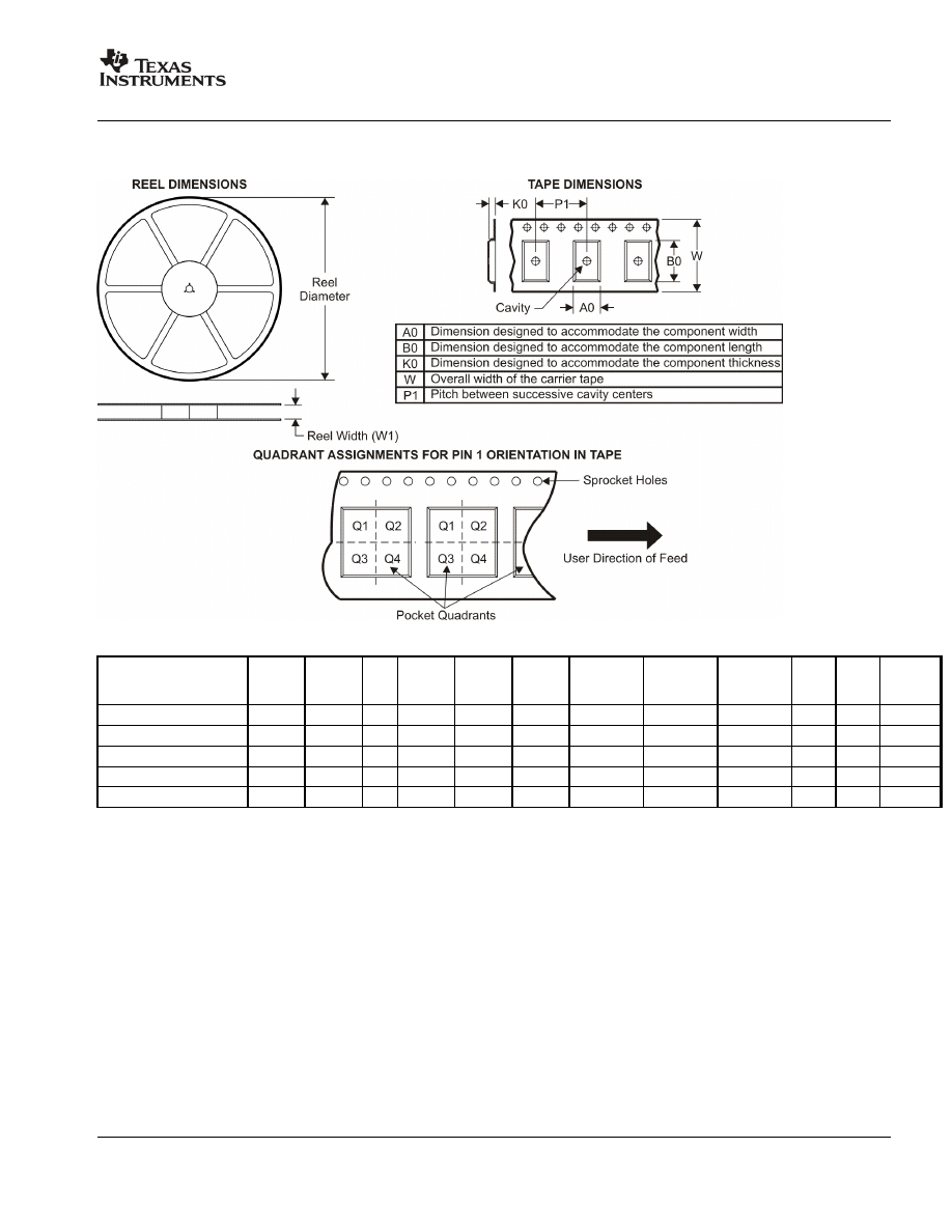
TAPE AND REEL INFORMATION
*All dimensions are nominal
Device
Package
Type
Package
Drawing
Pins
SPQ
Reel
Diameter
(mm)
Reel
Width
W1 (mm)
A0 (mm)
B0 (mm)
K0 (mm)
P1
(mm)
W
(mm)
Pin1
Quadrant
TLC7528CDWR
SOIC
DW
20
2000
330.0
24.4
10.8
13.1
2.65
12.0
24.0
Q1
TLC7528CPWR
TSSOP
PW
20
2000
330.0
16.4
6.95
7.1
1.6
8.0
16.0
Q1
TLC7528EDWR
SOIC
DW
20
2000
330.0
24.4
10.8
13.1
2.65
12.0
24.0
Q1
TLC7528IDWR
SOIC
DW
20
2000
330.0
24.4
10.8
13.1
2.65
12.0
24.0
Q1
TLC7528IPWR
TSSOP
PW
20
2000
330.0
16.4
6.95
7.1
1.6
8.0
16.0
Q1
PACKAGE MATERIALS INFORMATION
www.ti.com
11-Mar-2008
Pack Materials-Page 1
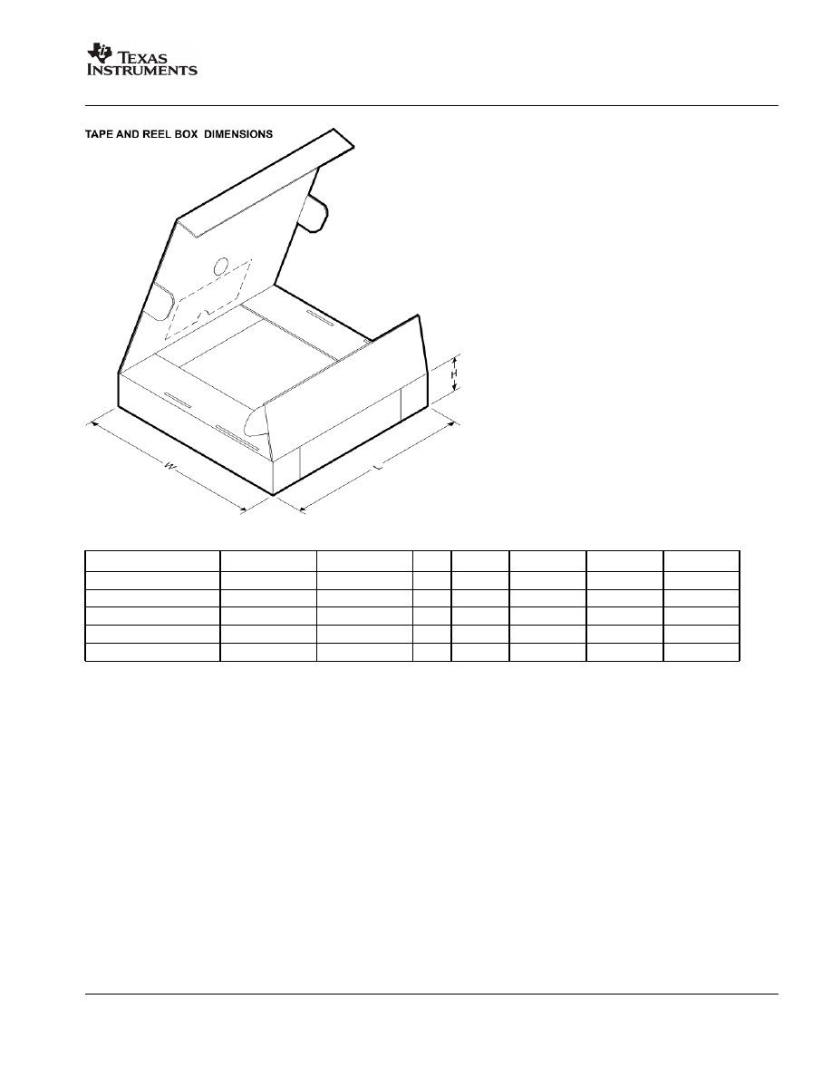
*All dimensions are nominal
Device
Package Type
Package Drawing
Pins
SPQ
Length (mm)
Width (mm)
Height (mm)
TLC7528CDWR
SOIC
DW
20
2000
346.0
346.0
41.0
TLC7528CPWR
TSSOP
PW
20
2000
346.0
346.0
33.0
TLC7528EDWR
SOIC
DW
20
2000
346.0
346.0
41.0
TLC7528IDWR
SOIC
DW
20
2000
346.0
346.0
41.0
TLC7528IPWR
TSSOP
PW
20
2000
346.0
346.0
33.0
PACKAGE MATERIALS INFORMATION
www.ti.com
11-Mar-2008
Pack Materials-Page 2
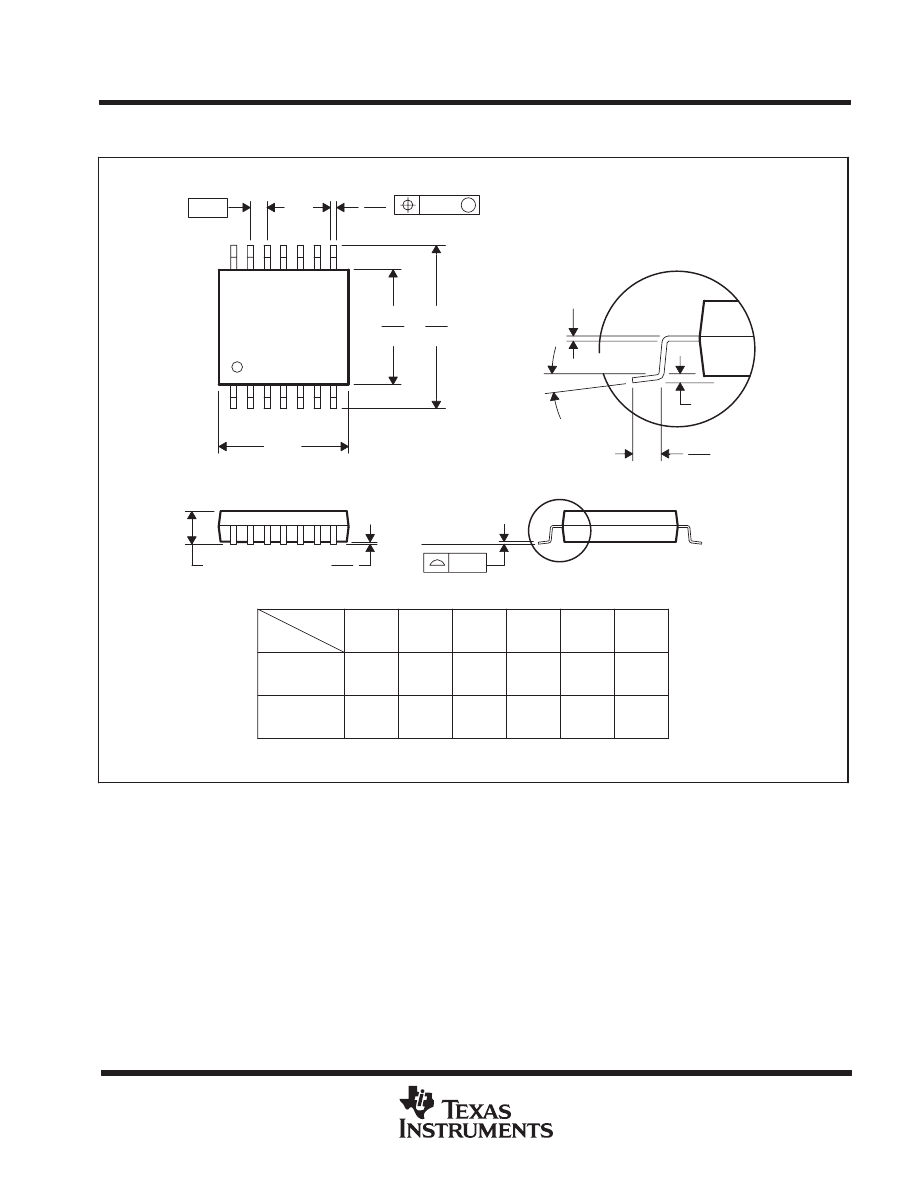
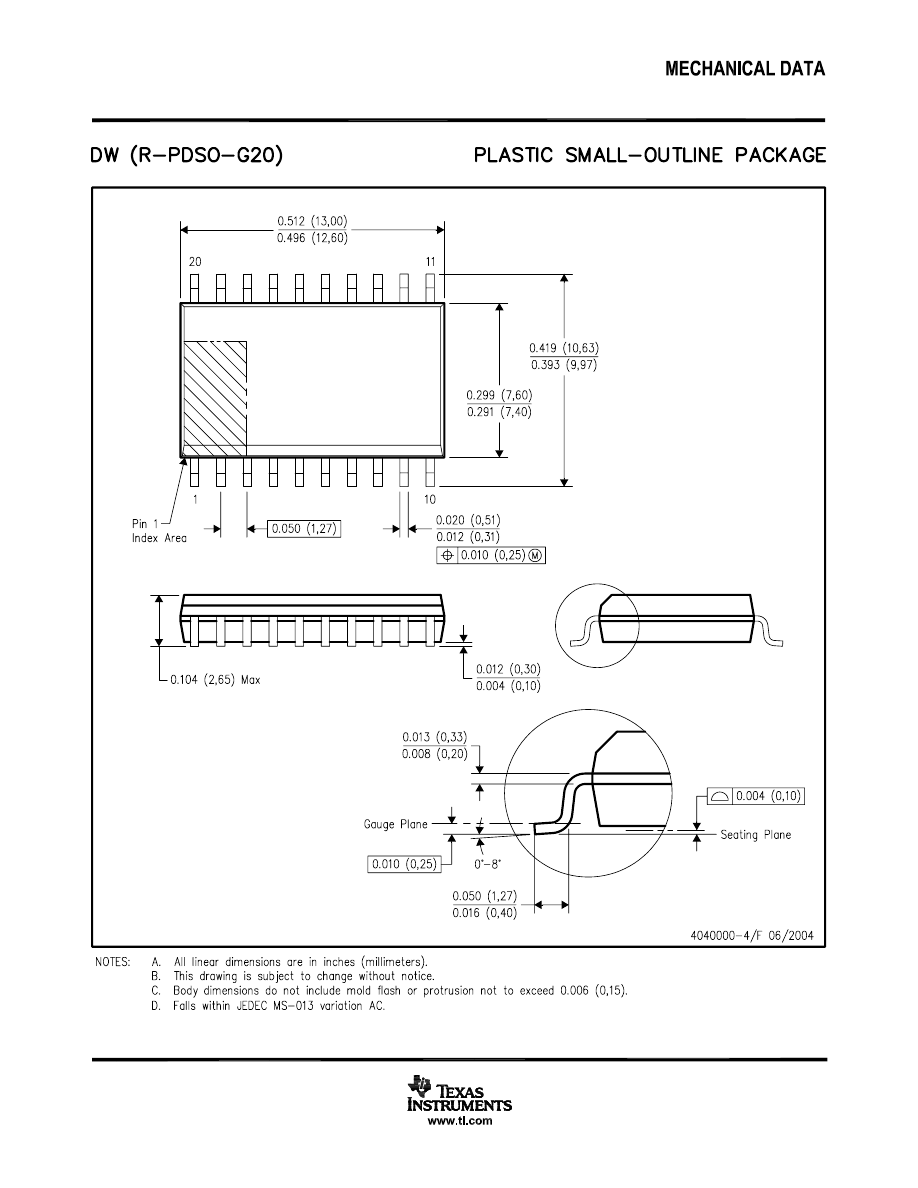
MECHANICAL DATA
MTSS001C – JANUARY 1995 – REVISED FEBRUARY 1999
POST OFFICE BOX 655303
•
DALLAS, TEXAS 75265
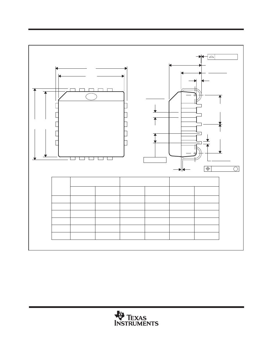
PW (R-PDSO-G**)
PLASTIC SMALL-OUTLINE PACKAGE
14 PINS SHOWN
0,65
M
0,10
0,10
0,25
0,50
0,75
0,15 NOM
Gage Plane
28
9,80
9,60
24
7,90
7,70
20
16
6,60
6,40
4040064/F 01/97
0,30
6,60
6,20
8
0,19
4,30
4,50
7
0,15
14
A
1
1,20 MAX
14
5,10
4,90
8
3,10
2,90
A MAX
A MIN
DIM
PINS **
0,05
4,90
5,10
Seating Plane
0
°
– 8
°
NOTES: A. All linear dimensions are in millimeters.
B. This drawing is subject to change without notice.
C. Body dimensions do not include mold flash or protrusion not to exceed 0,15.
D. Falls within JEDEC MO-153
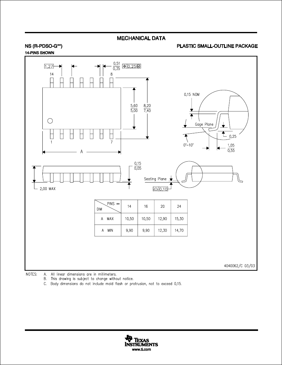
MECHANICAL DATA
MPLC004A – OCTOBER 1994
1
POST OFFICE BOX 655303
•
DALLAS, TEXAS 75265
FN (S-PQCC-J**)
PLASTIC J-LEADED CHIP CARRIER
4040005 / B 03/95
20 PIN SHOWN
0.026 (0,66)
0.032 (0,81)
D2 / E2
0.020 (0,51) MIN
0.180 (4,57) MAX
0.120 (3,05)
0.090 (2,29)
D2 / E2
0.013 (0,33)
0.021 (0,53)
Seating Plane
MAX
D2 / E2
0.219 (5,56)
0.169 (4,29)
0.319 (8,10)
0.469 (11,91)
0.569 (14,45)
0.369 (9,37)
MAX
0.356 (9,04)
0.456 (11,58)
0.656 (16,66)
0.008 (0,20) NOM
1.158 (29,41)
0.958 (24,33)
0.756 (19,20)
0.191 (4,85)
0.141 (3,58)
MIN
0.441 (11,20)
0.541 (13,74)
0.291 (7,39)
0.341 (8,66)
18
19
14
13
D
D1
1
3
9
E1
E
4
8
MIN
MAX
MIN
PINS
**
20
28
44
0.385 (9,78)
0.485 (12,32)
0.685 (17,40)
52
68
84
1.185 (30,10)
0.985 (25,02)
0.785 (19,94)
D / E
0.395 (10,03)
0.495 (12,57)
1.195 (30,35)
0.995 (25,27)
0.695 (17,65)
0.795 (20,19)
NO. OF
D1 / E1
0.350 (8,89)
0.450 (11,43)
1.150 (29,21)
0.950 (24,13)
0.650 (16,51)
0.750 (19,05)
0.004 (0,10)
M
0.007 (0,18)
0.050 (1,27)
NOTES: A. All linear dimensions are in inches (millimeters).
B. This drawing is subject to change without notice.
C. Falls within JEDEC MS-018

IMPORTANT NOTICE
Texas Instruments Incorporated and its subsidiaries (TI) reserve the right to make corrections, modifications, enhancements, improvements,
and other changes to its products and services at any time and to discontinue any product or service without notice. Customers should
obtain the latest relevant information before placing orders and should verify that such information is current and complete. All products are
sold subject to TI’s terms and conditions of sale supplied at the time of order acknowledgment.
TI warrants performance of its hardware products to the specifications applicable at the time of sale in accordance with TI’s standard
warranty. Testing and other quality control techniques are used to the extent TI deems necessary to support this warranty. Except where
mandated by government requirements, testing of all parameters of each product is not necessarily performed.
TI assumes no liability for applications assistance or customer product design. Customers are responsible for their products and
applications using TI components. To minimize the risks associated with customer products and applications, customers should provide
adequate design and operating safeguards.
TI does not warrant or represent that any license, either express or implied, is granted under any TI patent right, copyright, mask work right,
or other TI intellectual property right relating to any combination, machine, or process in which TI products or services are used. Information
published by TI regarding third-party products or services does not constitute a license from TI to use such products or services or a
warranty or endorsement thereof. Use of such information may require a license from a third party under the patents or other intellectual
property of the third party, or a license from TI under the patents or other intellectual property of TI.
Reproduction of TI information in TI data books or data sheets is permissible only if reproduction is without alteration and is accompanied
by all associated warranties, conditions, limitations, and notices. Reproduction of this information with alteration is an unfair and deceptive
business practice. TI is not responsible or liable for such altered documentation. Information of third parties may be subject to additional
restrictions.
Resale of TI products or services with statements different from or beyond the parameters stated by TI for that product or service voids all
express and any implied warranties for the associated TI product or service and is an unfair and deceptive business practice. TI is not
responsible or liable for any such statements.
TI products are not authorized for use in safety-critical applications (such as life support) where a failure of the TI product would reasonably
be expected to cause severe personal injury or death, unless officers of the parties have executed an agreement specifically governing
such use. Buyers represent that they have all necessary expertise in the safety and regulatory ramifications of their applications, and
acknowledge and agree that they are solely responsible for all legal, regulatory and safety-related requirements concerning their products
and any use of TI products in such safety-critical applications, notwithstanding any applications-related information or support that may be
provided by TI. Further, Buyers must fully indemnify TI and its representatives against any damages arising out of the use of TI products in
such safety-critical applications.
TI products are neither designed nor intended for use in military/aerospace applications or environments unless the TI products are
specifically designated by TI as military-grade or "enhanced plastic." Only products designated by TI as military-grade meet military
specifications. Buyers acknowledge and agree that any such use of TI products which TI has not designated as military-grade is solely at
the Buyer's risk, and that they are solely responsible for compliance with all legal and regulatory requirements in connection with such use.
TI products are neither designed nor intended for use in automotive applications or environments unless the specific TI products are
designated by TI as compliant with ISO/TS 16949 requirements. Buyers acknowledge and agree that, if they use any non-designated
products in automotive applications, TI will not be responsible for any failure to meet such requirements.
Following are URLs where you can obtain information on other Texas Instruments products and application solutions:
Products
Applications
Amplifiers
Audio
Data Converters
Automotive
DSP
Broadband
Clocks and Timers
Digital Control
Interface
Medical
Logic
Military
Power Mgmt
Optical Networking
Microcontrollers
Security
RFID
Telephony
RF/IF and ZigBee® Solutions
Video & Imaging
Wireless
Mailing Address: Texas Instruments, Post Office Box 655303, Dallas, Texas 75265
Copyright © 2008, Texas Instruments Incorporated
Wyszukiwarka
Podobne podstrony:
4063 (Texas Instruments) id 384 Nieznany (2)
NE555 Texas Instruments id 3161 Nieznany
ma741 Texas Instruments id 2757 Nieznany
TLC5945 (Texas Instruments)
TLC5922 (Texas Instruments)
TLC5923 (Texas Instruments)
TLC548, TLC549 (Texas Instruments)
NE555 Texas Instruments
TLC5941 (Texas Instruments)
TLC5921 (Texas Instruments)
TLC5920 (Texas Instruments)
TI89 TI92 Symbolic Math Guide Texas Instruments (2001) WW
LMV358 Texas Instruments
TIP74 (Texas Instruments)
ICL7135, TLC7135 (Texas Instruments)
więcej podobnych podstron