SLFS022E − SEPTEMBER 1973 − REVISED MARCH 2004
1
POST OFFICE BOX 655303
•
DALLAS, TEXAS 75265
D
Timing From Microseconds to Hours
D
Astable or Monostable Operation
D
Adjustable Duty Cycle
D
TTL-Compatible Output Can Sink or Source
Up To 200 mA
description/ordering information
These devices are precision timing circuits
capable of producing accurate time delays or
oscillation. In the time-delay or monostable mode
of operation, the timed interval is controlled by a
single external resistor and capacitor network. In
the astable mode of operation, the frequency and
duty cycle can be controlled independently with
two external resistors and a single external
capacitor.
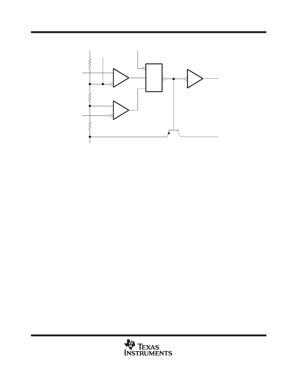
The threshold and trigger levels normally are
two-thirds and one-third, respectively, of V
CC
.
These levels can be altered by use of the
control-voltage terminal. When the trigger input
falls below the trigger level, the flip-flop is set and
the output goes high. If the trigger input is above
the trigger level and the threshold input is above
the threshold level, the flip-flop is reset and
the output is low. The reset (RESET) input can override all other inputs and can be used to initiate a new timing
cycle. When RESET goes low, the flip-flop is reset and the output goes low. When the output is low, a
low-impedance path is provided between discharge (DISCH) and ground.
The output circuit is capable of sinking or sourcing current up to 200 mA. Operation is specified for supplies of
5 V to 15 V. With a 5-V supply, output levels are compatible with TTL inputs.
Copyright
2004, Texas Instruments Incorporated
!
" #
$%! & %
& !
1
2
3
4
8
7
6
5
GND
TRIG
OUT
RESET
V
CC
DISCH
THRES
CONT
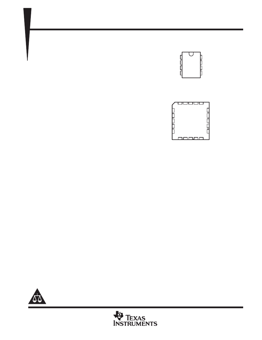
NE555 . . . D, P, PS, OR PW PACKAGE
SA555 . . . D OR P PACKAGE
SE555 . . . D, JG, OR P PACKAGE
(TOP VIEW)
3
2
1 20 19
9 10 11 12 13
4
5
6
7
8
18
17
16
15
14
NC
DISCH
NC
THRES
NC
NC
TRIG
NC
OUT
NC
SE555 . . . FK PACKAGE
(TOP VIEW)
NC
GND
NC
CONT
NC
VCC
NC
NC
RESET
NC
NC − No internal connection
'()(*+*
"$ ! "
& % & !
Please be aware that an important notice concerning availability, standard warranty, and use in critical applications of
Texas Instruments semiconductor products and disclaimers thereto appears at the end of this data sheet.
SLFS022E − SEPTEMBER 1973 − REVISED MARCH 2004
2
POST OFFICE BOX 655303
•
DALLAS, TEXAS 75265
description/ordering information (continued)
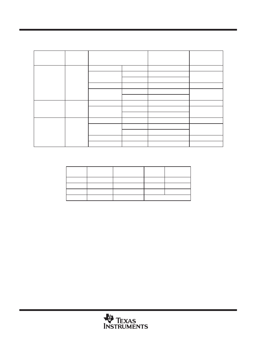
ORDERING INFORMATION
TA
VTHRES
MAX
VCC = 15 V
PACKAGE†
ORDERABLE
PART NUMBER
TOP-SIDE
MARKING
PDIP (P)
Tube of 50
NE555P
NE555P
SOIC (D)
Tube of 75
NE555D
NE555
0
°
C to 70
°
C
11.2 V
SOIC (D)
Reel of 2500
NE555DR
NE555
0
°
C to 70
°
C
11.2 V
SOP (PS)
Reel of 2000
NE555PSR
N555
TSSOP (PW)
Tube of 150
NE555PW
N555
TSSOP (PW)
Reel of 2000
NE555PWR
N555
PDIP (P)
Tube of 50
SA555P
SA555P
−40
°
C to 85
°
C
11.2 V
SOIC (D)
Tube of 75
SA555D
SA555
−40 C to 85 C
11.2 V
SOIC (D)
Reel of 2000
SA555DR
SA555
PDIP (P)
Tube of 50
SE555P
SE555P
SOIC (D)
Tube of 75
SE555D
SE555D
− 55
°
C to 125
°
C
10.6 V
SOIC (D)
Reel of 2500
SE555DR
SE555D
− 55 C to 125 C
10.6 V
CDIP (JG)
Tube of 50
SE555JG
SE555JG
LCCC (FK)
Tube of55
SE555FK
SE555FK
† Package drawings, standard packing quantities, thermal data, symbolization, and PCB design guidelines are available at
www.ti.com/sc/package.
FUNCTION TABLE
RESET
TRIGGER
VOLTAGE‡
THRESHOLD
VOLTAGE‡
OUTPUT
DISCHARGE
SWITCH
Low
Irrelevant
Irrelevant
Low
On
High
<1/3 VDD
Irrelevant
High
Off
High
>1/3 VDD
>2/3 VDD
Low
On
High
>1/3 VDD
<2/3 VDD
As previously established
‡ Voltage levels shown are nominal.
SLFS022E − SEPTEMBER 1973 − REVISED MARCH 2004
3
POST OFFICE BOX 655303
•
DALLAS, TEXAS 75265
functional block diagram
1
S
R
R1
TRIG
THRES
VCC
CONT
RESET
OUT
DISCH
GND
ÎÎ
Î
Î
Î
Î
Î
Î
Î
Pin numbers shown are for the D, JG, P, PS, and PW packages.
NOTE A: RESET can override TRIG, which can override THRES.
4
8
5
6
2
1
7
3
SLFS022E − SEPTEMBER 1973 − REVISED MARCH 2004
4
POST OFFICE BOX 655303
•
DALLAS, TEXAS 75265
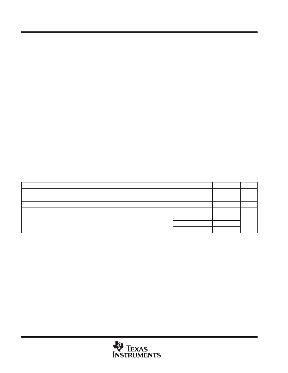
absolute maximum ratings over operating free-air temperature range (unless otherwise noted)
†
Supply voltage, V
CC
(see Note 1)
18 V
. . . . . . . . . . . . . . . . . . . . . . . . . . . . . . . . . . . . . . . . . . . . . . . . . . . . . . . . . . . .
Input voltage (CONT, RESET, THRES, and TRIG)
V
CC
. . . . . . . . . . . . . . . . . . . . . . . . . . . . . . . . . . . . . . . . . . . . . .
Output current
±
225 mA
. . . . . . . . . . . . . . . . . . . . . . . . . . . . . . . . . . . . . . . . . . . . . . . . . . . . . . . . . . . . . . . . . . . . . . . . .
Package thermal impedance,
θ
JA
(see Notes 2 and 3): D package
97
°
C/W
. . . . . . . . . . . . . . . . . . . . . . . . . . . .
P package
85
°
C/W
. . . . . . . . . . . . . . . . . . . . . . . . . . . .
PS package
95
°
C/W
. . . . . . . . . . . . . . . . . . . . . . . . . . .
PW package
149
°
C/W
. . . . . . . . . . . . . . . . . . . . . . . . .
Package thermal impedance,
θ
JC
(see Notes 4 and 5): FK package
5.61
°
C/W
. . . . . . . . . . . . . . . . . . . . . . . . .
JG package
14.5
°
C/W
. . . . . . . . . . . . . . . . . . . . . . . . .
Operating virtual junction temperature, T
J
150
°
C
. . . . . . . . . . . . . . . . . . . . . . . . . . . . . . . . . . . . . . . . . . . . . . . . . . .
Case temperature for 60 seconds: FK package
260
°
C
. . . . . . . . . . . . . . . . . . . . . . . . . . . . . . . . . . . . . . . . . . . . . .
Lead temperature 1,6 mm (1/16 inch) from case for 60 seconds: JG package
300
°
C
. . . . . . . . . . . . . . . . . . .
Storage temperature range, T
stg
−65
°
C to 150
°
C
. . . . . . . . . . . . . . . . . . . . . . . . . . . . . . . . . . . . . . . . . . . . . . . . . . .
† Stresses beyond those listed under “absolute maximum ratings” may cause permanent damage to the device. These are stress ratings only, and
functional operation of the device at these or any other conditions beyond those indicated under “recommended operating conditions” is not
implied. Exposure to absolute-maximum-rated conditions for extended periods may affect device reliability.
NOTES:
1. All voltage values are with respect to GND.
2. Maximum power dissipation is a function of TJ(max),
θ
JA, and TA. The maximum allowable power dissipation at any allowable
ambient temperature is PD = (TJ(max) − TA)/
θ
JA. Operating at the absolute maximum TJ of 150
°
C can affect reliability.
3. The package thermal impedance is calculated in accordance with JESD 51-7.
4. Maximum power dissipation is a function of TJ(max),
θ
JC, and TC. The maximum allowable power dissipation at any allowable case
temperature is PD = (TJ(max) − TC)/
θ
JC. Operating at the absolute maximum TJ of 150
°
C can affect reliability.
5. The package thermal impedance is calculated in accordance with MIL-STD-883.
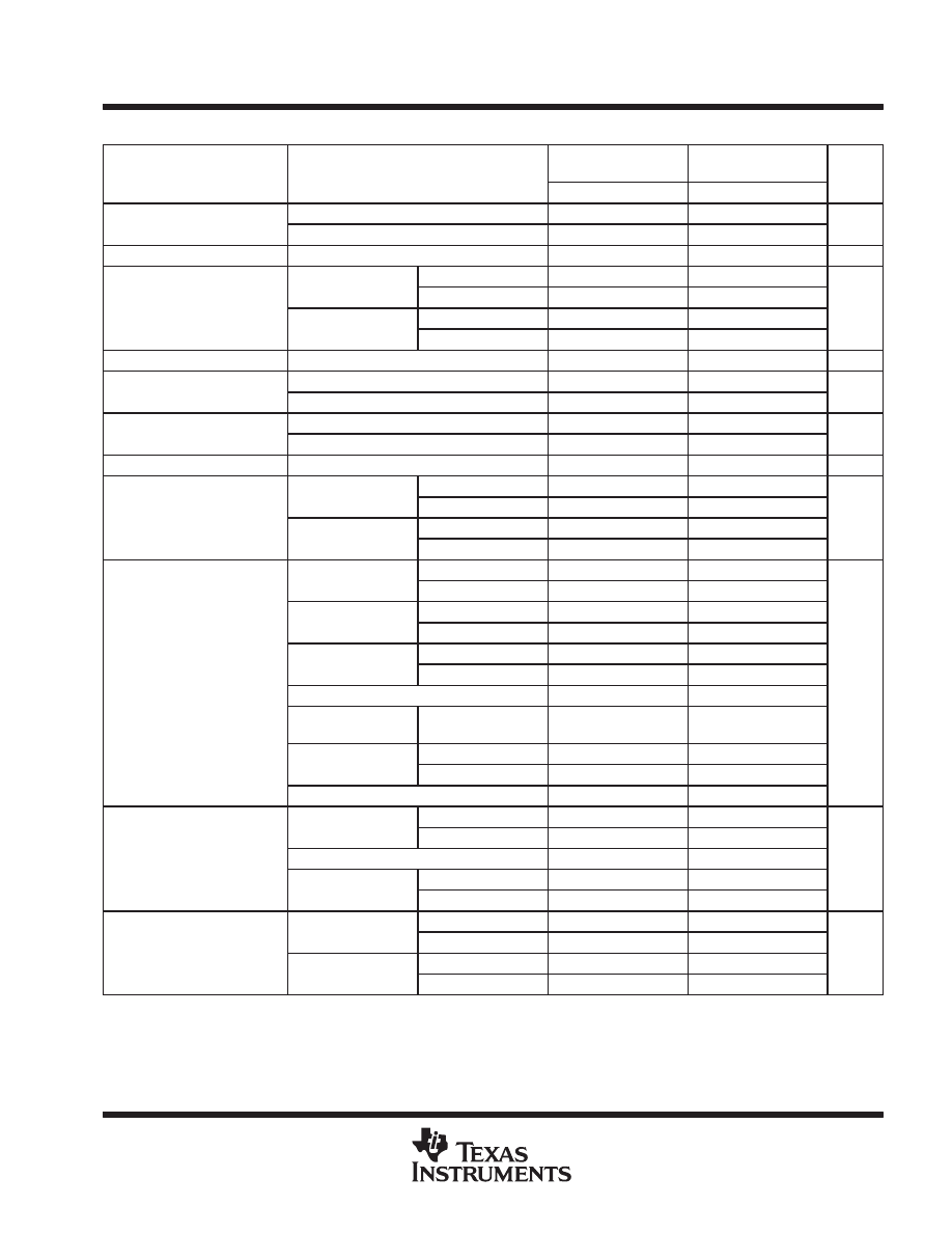
recommended operating conditions
MIN
MAX
UNIT
VCC
Supply voltage
SA555, NE555
4.5
16
V
VCC
Supply voltage
SE555
4.5
18
V
VI
Input voltage (CONT, RESET, THRES, and TRIG)
VCC
V
IO
Output current
±
200
mA
NE555
0
70
TA
Operating free-air temperature
SA555
−40
85
°
C
TA
Operating free-air temperature
SE555
−55
125
C
SLFS022E − SEPTEMBER 1973 − REVISED MARCH 2004
5
POST OFFICE BOX 655303
•
DALLAS, TEXAS 75265
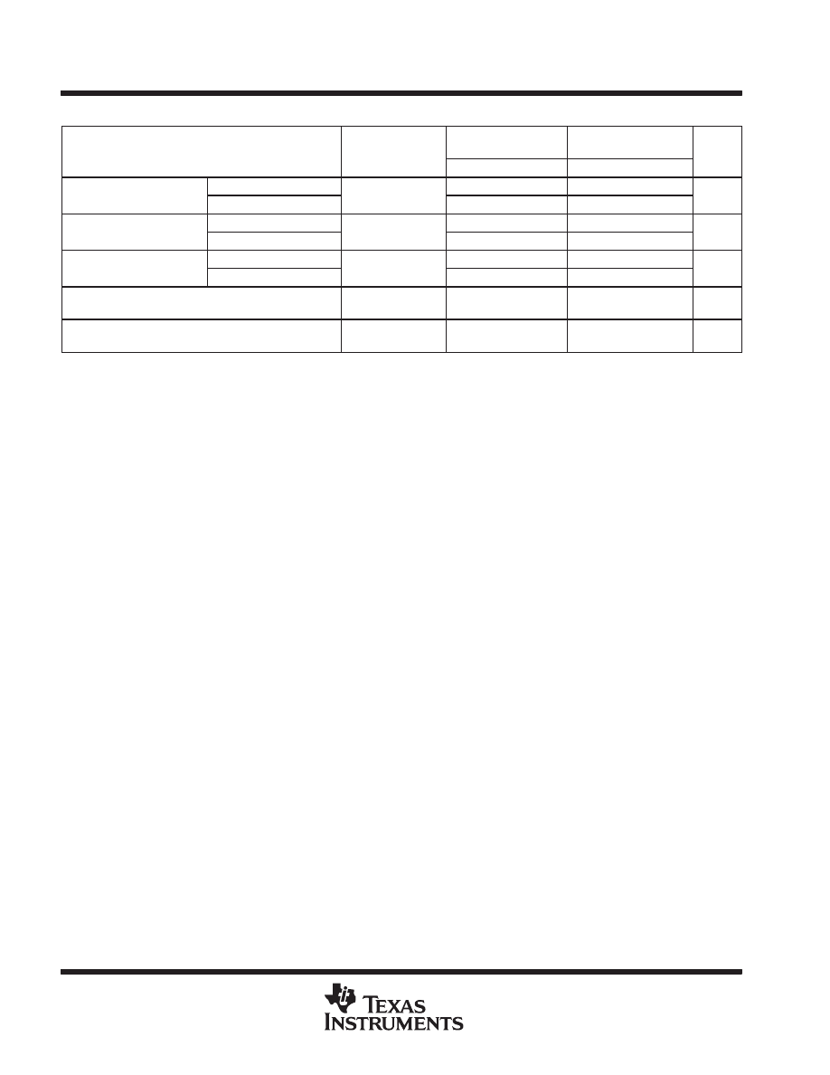
electrical characteristics, V
CC
= 5 V to 15 V, T
A
= 25
°
C (unless otherwise noted)
PARAMETER
TEST CONDITIONS
SE555
NE555
SA555
UNIT
PARAMETER
TEST CONDITIONS
MIN
TYP
MAX
MIN
TYP
MAX
UNIT
THRES voltage level
VCC = 15 V
9.4
10
10.6
8.8
10
11.2
V
THRES voltage level
VCC = 5 V
2.7
3.3
4
2.4
3.3
4.2
V
THRES current (see Note 6)
30
250
30
250
nA
VCC = 15 V
4.8
5
5.2
4.5
5
5.6
TRIG voltage level
VCC = 15 V
TA = −55
°
C to 125
°
C
3
6
V
TRIG voltage level
VCC = 5 V
1.45
1.67
1.9
1.1
1.67
2.2
V
VCC = 5 V
TA = −55
°
C to 125
°
C
1.9
TRIG current
TRIG at 0 V
0.5
0.9
0.5
2
µ
A
RESET voltage level
0.3
0.7
1
0.3
0.7
1
V
RESET voltage level
TA = −55
°
C to 125
°
C
1.1
V
RESET current
RESET at VCC
0.1
0.4
0.1
0.4
mA
RESET current
RESET at 0 V
−0.4
−1
−0.4
−1.5
mA
DISCH switch off-state current
20
100
20
100
nA
VCC = 15 V
9.6
10
10.4
9
10
11
CONT voltage (open circuit)
VCC = 15 V
TA = −55
°
C to 125
°
C
9.6
10.4
V
CONT voltage (open circuit)
VCC = 5 V
2.9
3.3
3.8
2.6
3.3
4
V
VCC = 5 V
TA = −55
°
C to 125
°
C
2.9
3.8
VCC = 15 V,
0.1
0.15
0.1
0.25
VCC = 15 V,
IOL = 10 mA
TA = −55
°
C to 125
°
C
0.2
VCC = 15 V,
0.4
0.5
0.4
0.75
VCC = 15 V,
IOL = 50 mA
TA = −55
°
C to 125
°
C
1
VCC = 15 V,
2
2.2
2
2.5
Low-level output voltage
VCC = 15 V,
IOL = 100 mA
TA = −55
°
C to 125
°
C
2.7
V
Low-level output voltage
VCC = 15 V,
IOL = 200 mA
2.5
2.5
V
VCC = 5 V,
IOL = 3.5 mA
TA = −55
°
C to 125
°
C
0.35
VCC = 5 V,
0.1
0.2
0.1
0.35
VCC = 5 V,
IOL = 5 mA
TA = −55
°
C to 125
°
C
0.8
VCC = 5 V,
IOL = 8 mA
0.15
0.25
0.15
0.4
VCC = 15 V,
13
13.3
12.75
13.3
VCC = 15 V,
IOH = −100 mA
TA = −55
°
C to 125
°
C
12
High-level output voltage
VCC = 15 V,
IOH = −200 mA
12.5
12.5
V
High-level output voltage
VCC = 5 V,
3
3.3
2.75
3.3
V
VCC = 5 V,
IOH = −100 mA
TA = −55
°
C to 125
°
C
2
Output low,
VCC = 15 V
10
12
10
15
Supply current
Output low,
No load
VCC = 5 V
3
5
3
6
mA
Supply current
Output high,
VCC = 15 V
9
10
9
13
mA
Output high,
No load
VCC = 5 V
2
4
2
5
NOTE 6: This parameter influences the maximum value of the timing resistors RA and RB in the circuit of Figure 12. For example, when
VCC = 5 V, the maximum value is R = RA + RB
≈
3.4 M
Ω
, and for VCC = 15 V, the maximum value is 10 M
Ω.
SLFS022E − SEPTEMBER 1973 − REVISED MARCH 2004
6
POST OFFICE BOX 655303
•
DALLAS, TEXAS 75265
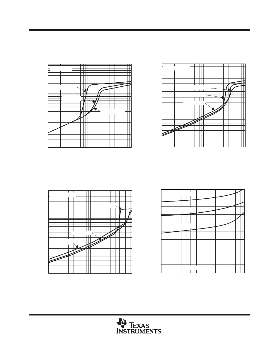
operating characteristics, V
CC
= 5 V and 15 V
PARAMETER
TEST
CONDITIONS†
SE555
NE555
SA555
UNIT
PARAMETER
CONDITIONS†
MIN
TYP
MAX
MIN
TYP
MAX
UNIT
Initial error
‡
Each timer, monostable§
TA = 25
°
C
0.5
1.5*
1
3
%
Initial error
of timing interval‡
Each timer, astable¶
TA = 25
°
C
1.5
2.25
%
Temperature coefficient
Each timer, monostable§
TA = MIN to MAX
30
100*
50
ppm/
°
C
Temperature coefficient
of timing interval
Each timer, astable¶
TA = MIN to MAX
90
150
ppm/
°
C
Supply-voltage sensitivity
Each timer, monostable§
TA = 25
°
C
0.05
0.2*
0.1
0.5
%/V
Supply-voltage sensitivity
of timing interval
Each timer, astable¶
TA = 25
°
C
0.15
0.3
%/V
Output-pulse rise time
CL = 15 pF,
TA = 25
°
C
100
200*
100
300
ns
Output-pulse fall time
CL = 15 pF,
TA = 25
°
C
100
200*
100
300
ns
* On products compliant to MIL-PRF-38535, this parameter is not production tested.
† For conditions shown as MIN or MAX, use the appropriate value specified under recommended operating conditions.
‡ Timing interval error is defined as the difference between the measured value and the average value of a random sample from each process
run.
§ Values specified are for a device in a monostable circuit similar to Figure 9, with the following component values: RA = 2 k
Ω
to 100 k
Ω
,
C = 0.1
µ
F.
¶ Values specified are for a device in an astable circuit similar to Figure 12, with the following component values: RA = 1 k
Ω
to 100 k
Ω
,
C = 0.1
µ
F.
SLFS022E − SEPTEMBER 1973 − REVISED MARCH 2004
7
POST OFFICE BOX 655303
•
DALLAS, TEXAS 75265
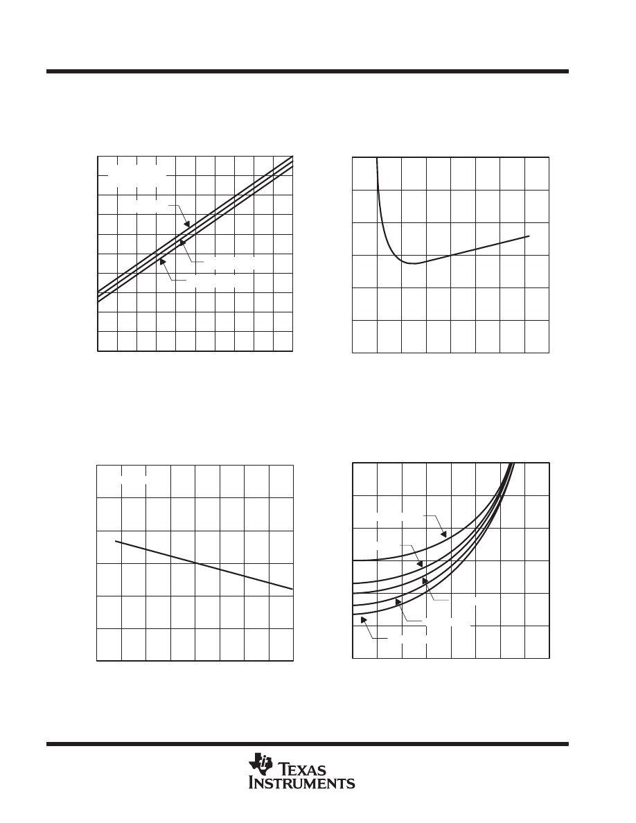
TYPICAL CHARACTERISTICS
†
Figure 1
ÏÏÏÏ
TA = 125
°
C
ÏÏÏ
TA = 25
°
C
IOL − Low-Level Output Current − mA
ÏÏÏÏ
VCC = 5 V
LOW-LEVEL OUTPUT VOLTAGE
vs
LOW-LEVEL OUTPUT CURRENT
ÏÏÏÏÏ
ÏÏÏÏÏ
TA = −55
°
C
0.1
0.04
0.01
1
2
4
7
10
20
40
70 100
0.07
1
0.4
0.7
10
4
7
0.02
0.2
2
− Low-Level Output V
o
ltage − V
V
OL
Figure 2
ÏÏÏÏÏ
ÏÏÏÏÏ
VCC = 10 V
LOW-LEVEL OUTPUT VOLTAGE
vs
LOW-LEVEL OUTPUT CURRENT
− Low-Level Output V
o
ltage − V
V
OL
IOL − Low-Level Output Current − mA
0.1
0.04
0.01
1
2
4
7
10
20
40
70 100
0.07
1
0.4
0.7
10
4
7
0.02
0.2
2
ÏÏÏÏ
ÏÏÏÏ
TA = 125
°
C
ÏÏÏÏ
ÏÏÏÏ
TA = 25
°
C
ÏÏÏÏ
ÏÏÏÏ
TA= −55
°
C
Figure 3
TA = 125
°
C
TA = 25
°
C
TA = −55
°
C
ÏÏÏÏÏ
ÏÏÏÏÏ
VCC = 15 V
LOW-LEVEL OUTPUT VOLTAGE
vs
LOW-LEVEL OUTPUT CURRENT
− Low-Level Output V
o
ltage − V
V
OL
IOL − Low-Level Output Current − mA
0.1
0.04
0.01
1
2
4
7
10
20
40
70 100
0.07
1
0.4
0.7
10
4
7
0.02
0.2
2
Figure 4
1
0.6
0.2
0
1.4
1.8
2.0
0.4
1.6
0.8
1.2
−
IOH − High-Level Output Current − mA
ÏÏÏÏ
TA = 125
°
C
ÏÏÏÏ
ÏÏÏÏ
TA = 25
°
C
100
70
40
20
10
7
4
2
1
ÏÏÏÏÏÏ
ÏÏÏÏÏÏ
VCC = 5 V to 15 V
ÏÏÏÏ
TA = −55
°
C
DROP BETWEEN SUPPLY VOLTAGE AND OUTPUT
vs
HIGH-LEVEL OUTPUT CURRENT
V
CC
V
OH
−
V
oltage Drop − V
)
(
†Data for temperatures below 0
°
C and above 70
°
C are applicable for SE555 circuits only.
SLFS022E − SEPTEMBER 1973 − REVISED MARCH 2004
8
POST OFFICE BOX 655303
•
DALLAS, TEXAS 75265
TYPICAL CHARACTERISTICS
†
Figure 5
5
4
2
1
0
9
3
5
6
7
8
9
10
11
− Supply Current − mA
7
6
8
SUPPLY CURRENT
vs
SUPPLY VOLTAGE
10
12
13
14
15
TA = 25
°
C
TA = 125
°
C
TA = −55
°
C
Output Low,
No Load
CCI
VCC − Supply Voltage − V
Figure 6
1
0.995
0.990
0.985
0
5
10
1.005
1.010
NORMALIZED OUTPUT PULSE DURATION
(MONOSTABLE OPERATION)
vs
SUPPLY VOLTAGE
1.015
15
20
CC
V
Pulse Duration Relative to V
alue at = 10 V
VCC − Supply Voltage − V
Figure 7
1
0.995
0.990
0.985
−75
−25
25
1.005
1.010
NORMALIZED OUTPUT PULSE DURATION
(MONOSTABLE OPERATION)
vs
FREE-AIR TEMPERATURE
1.015
75
125
Pulse Duration Relative to V
alue at = 25
TA − Free-Air Temperature −
°
C
−50
0
50
100
VCC = 10 V
T A
C
°
Figure 8
150
100
50
0
200
250
300
− Propagation Delay T
ime − ns
PROPAGATION DELAY TIME
vs
LOWEST VOLTAGE LEVEL
OF TRIGGER PULSE
Lowest Voltage Level of Trigger Pulse
TA = −55
°
C
TA = 125
°
C
TA = 25
°
C
t PD
TA = 0
°
C
TA = 70
°
C
0
0.1 x VCC
0.2 x VCC 0.3 x VCC
0.4 x VCC
†Data for temperatures below 0
°
C and above 70
°
C are applicable for SE555 series circuits only.
SLFS022E − SEPTEMBER 1973 − REVISED MARCH 2004
9
POST OFFICE BOX 655303
•
DALLAS, TEXAS 75265
APPLICATION INFORMATION
monostable operation
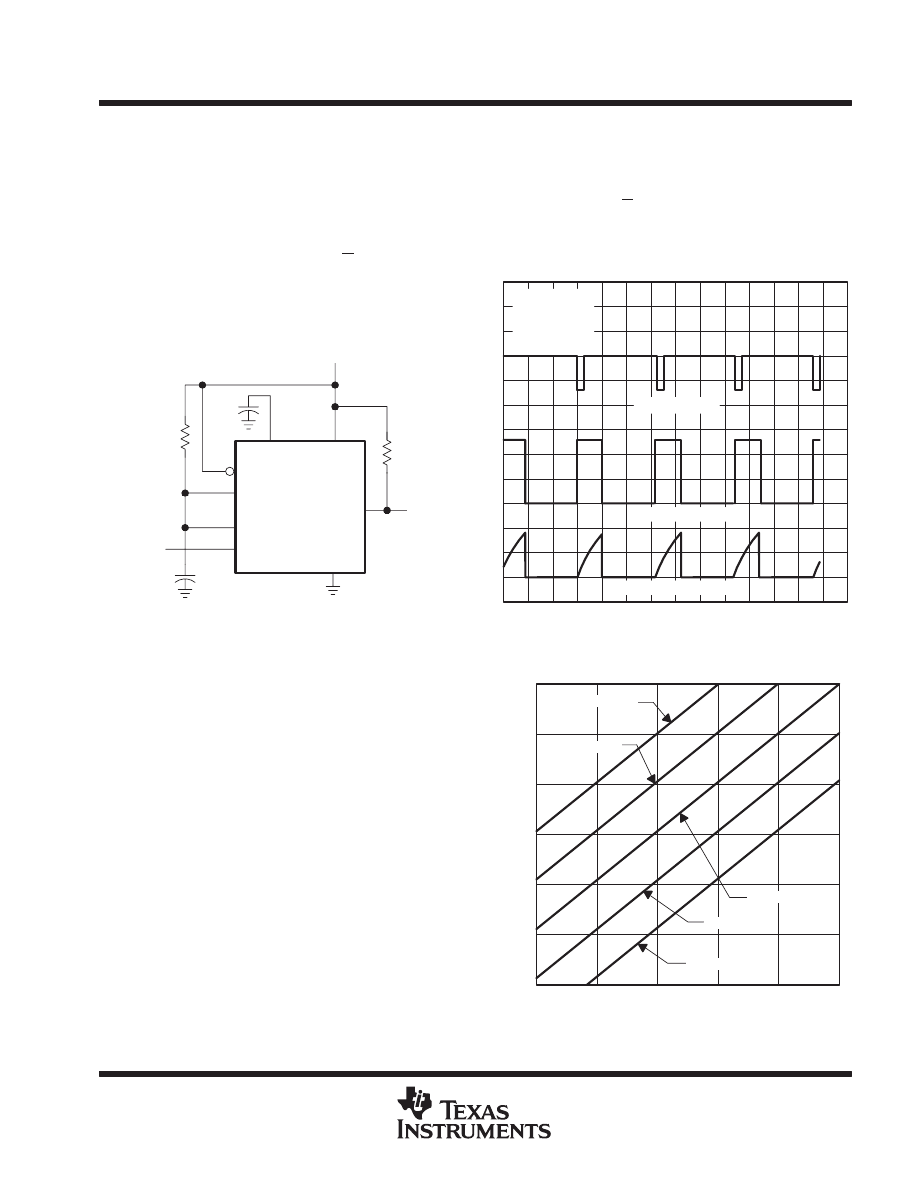
For monostable operation, any of these timers can be connected as shown in Figure 9. If the output is low,
application of a negative-going pulse to the trigger (TRIG) sets the flip-flop (Q goes low), drives the output high,
and turns off Q1. Capacitor C then is charged through R
A
until the voltage across the capacitor reaches the
threshold voltage of the threshold (THRES) input. If TRIG has returned to a high level, the output of the threshold
comparator resets the flip-flop (Q goes high), drives the output low, and discharges C through Q1.
VCC
(5 V to 15 V)
RA
RL
Output
GND
OUT
VCC
CONT
RESET
DISCH
THRES
TRIG
Input
ÎÎ
5
8
4
7
6
2
3
1
Pin numbers shown are for the D, JG, P, PS, and PW packages.
Figure 9. Circuit for Monostable Operation
V
oltage − 2 V/div
Time − 0.1 ms/div
ÏÏÏÏÏÏ
Capacitor Voltage
Output Voltage
Input Voltage
ÏÏÏÏÏ
ÏÏÏÏÏ
ÏÏÏÏÏ
ÏÏÏÏÏ
RA = 9.1 k
Ω
CL
= 0.01
µ
F
RL = 1 k
Ω
See Figure 9
Figure 10. Typical Monostable Waveforms
Monostable operation is initiated when TRIG
voltage falls below the trigger threshold. Once
initiated, the sequence ends only if TRIG is high
at the end of the timing interval. Because of the
threshold level and saturation voltage of Q1,
the output pulse duration is approximately
t
w
= 1.1R
A
C. Figure 11 is a plot of the time
constant for various values of R
A
and C. The
threshold levels and charge rates both are directly
proportional to the supply voltage, V
CC.
The timing
interval is, therefore, independent of the supply
voltage, so long as the supply voltage is constant
during the time interval.
Applying a negative-going trigger pulse
simultaneously to RESET and TRIG during the
timing interval discharges C and reinitiates the
cycle, commencing on the positive edge of the
reset pulse. The output is held low as long as the
reset pulse is low. To prevent false triggering,
when RESET is not used, it should be connected
to V
CC
.
− Output Pulse Duration − s
C − Capacitance −
µ
F
10
1
10−1
10−2
10−3
10−4
100
10
1
0.1
0.01
10−5
0.001
t w
RA = 10 M
Ω
RA = 10 k
Ω
RA = 1 k
Ω
RA = 100 k
Ω
RA = 1 M
Ω
Figure 11. Output Pulse Duration vs Capacitance
SLFS022E − SEPTEMBER 1973 − REVISED MARCH 2004
10
POST OFFICE BOX 655303
•
DALLAS, TEXAS 75265
APPLICATION INFORMATION
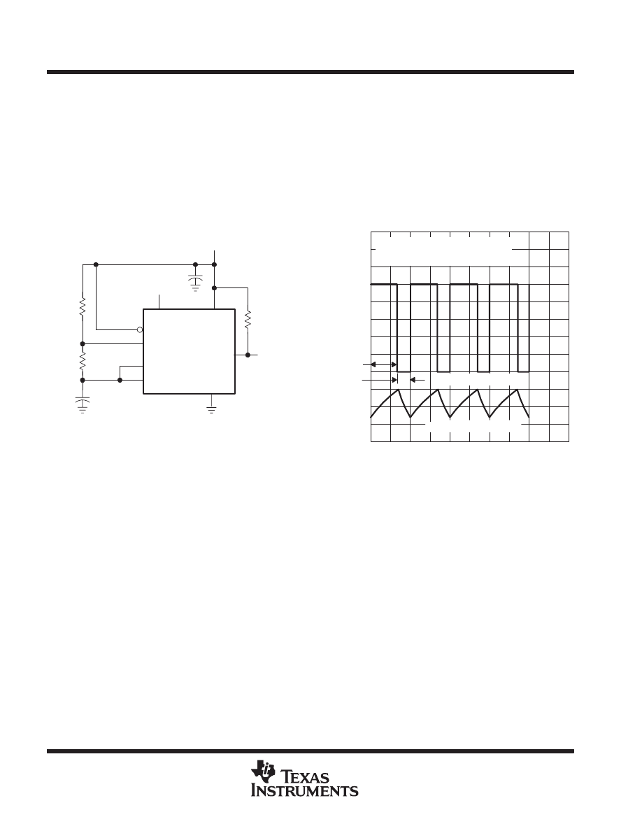
astable operation
As shown in Figure 12, adding a second resistor, R
B,
to the circuit of Figure 9 and connecting the trigger input
to the threshold input causes the timer to self-trigger and run as a multivibrator. The capacitor C charges through
R
A
and R
B
and then discharges through R
B
only. Therefore, the duty cycle is controlled by the values of R
A
and
R
B.
This astable connection results in capacitor C charging and discharging between the threshold-voltage level
(
≈
0.67
×
V
CC
) and the trigger-voltage level (
≈
0.33
×
V
CC
). As in the monostable circuit, charge and discharge
times (and, therefore, the frequency and duty cycle) are independent of the supply voltage.
GND
OUT
VCC
CONT
RESET
DISCH
THRES
TRIG
C
RB
RA
Output
RL
0.01
µ
F
VCC
(5 V to 15 V)
(see Note A)
Î
NOTE A: Decoupling CONT voltage to ground with a capacitor can
improve operation. This should be evaluated for individual
applications.
Open
5
8
4
7
6
2
3
1
Pin numbers shown are for the D, JG, P, PS, and PW packages.
Figure 12. Circuit for Astable Operation
V
oltage − 1 V/div
Time − 0.5 ms/div
t
H
Capacitor Voltage
Output Voltage
tL
ÏÏÏÏÏÏÏÏÏ
ÏÏÏÏÏÏÏÏÏ
ÏÏÏÏÏÏÏÏÏ
RA = 5 k
W
RL = 1 k
W
RB = 3 k
W
See Figure 12
C = 0.15
µ
F
Figure 13. Typical Astable Waveforms
SLFS022E − SEPTEMBER 1973 − REVISED MARCH 2004
11
POST OFFICE BOX 655303
•
DALLAS, TEXAS 75265
APPLICATION INFORMATION
astable operation (continued)
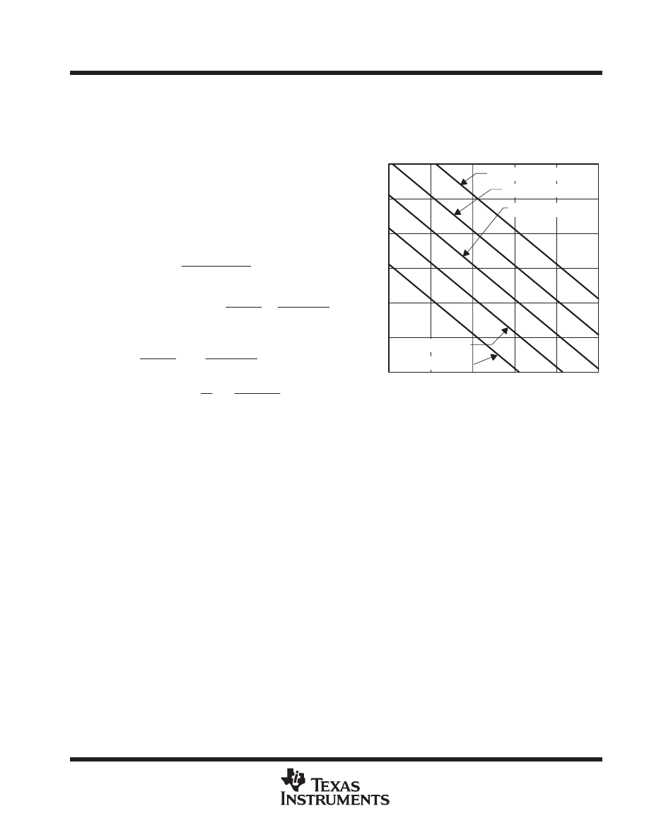
Figure 13 shows typical waveforms generated during astable operation. The output high-level duration t
H
and
low-level duration t
L
can be calculated as follows:
t
H
+
0.693 (R
A
)
R
B)
C
t
L
+
0.693 (R
B)
C
Other useful relationships are shown below.
period
+
t
H
)
t
L
+
0.693 (R
A
)
2R
B
) C
frequency
[
1.44
(R
A
)
2R
B
) C
Output driver duty cycle
+
t
L
t
H
)
t
L
+
R
B
R
A
)
2R
B
Output waveform duty cycle
+
t
L
t
H
+
R
B
R
A
)
R
B
Low-to-high ratio
+
t
H
t
H
)
t
L
+
1–
R
B
R
A
)
2R
B
f − Free-Running Frequency − Hz
C − Capacitance −
µ
F
100 k
10 k
1 k
100
10
1
100
10
1
0.1
0.01
0.1
0.001
RA + 2 RB = 10 M
Ω
RA + 2 RB = 1 M
Ω
RA + 2 RB = 100 k
Ω
RA + 2 RB = 10 k
Ω
RA + 2 RB = 1 k
Ω
Figure 14. Free-Running Frequency
SLFS022E − SEPTEMBER 1973 − REVISED MARCH 2004
12
POST OFFICE BOX 655303
•
DALLAS, TEXAS 75265
APPLICATION INFORMATION
missing-pulse detector
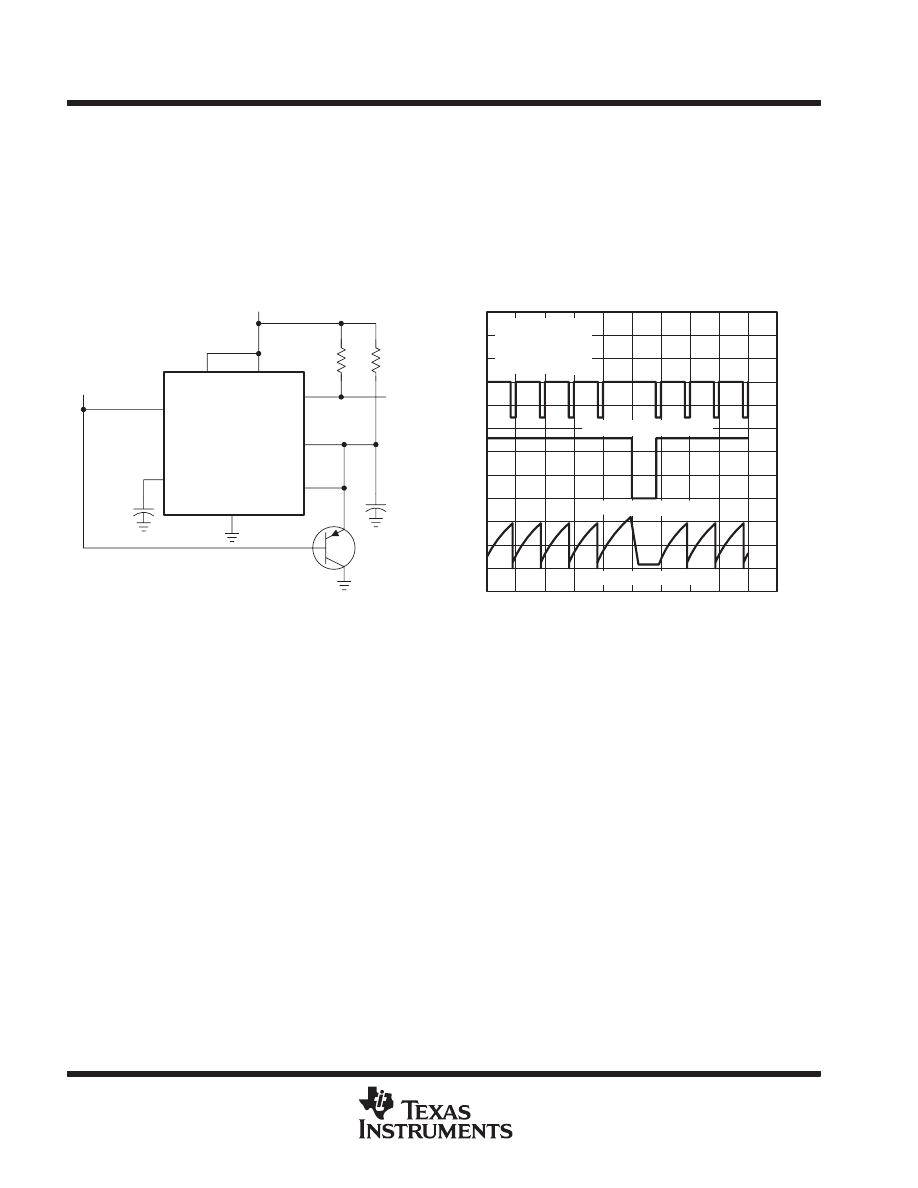
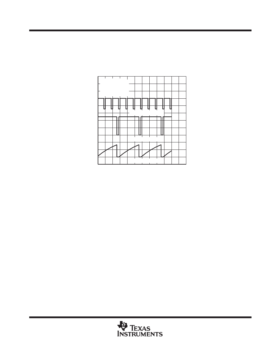
The circuit shown in Figure 15 can be used to detect a missing pulse or abnormally long spacing between
consecutive pulses in a train of pulses. The timing interval of the monostable circuit is retriggered continuously
by the input pulse train as long as the pulse spacing is less than the timing interval. A longer pulse spacing,
missing pulse, or terminated pulse train permits the timing interval to be completed, thereby generating an
output pulse as shown in Figure 16.
Figure 15. Circuit for Missing-Pulse Detector
VCC (5 V to 15 V)
DISCH
OUT
VCC
RESET
RL
RA
A5T3644
C
THRES
GND
CONT
TRIG
Input
0.01
µ
F
ÏÏÏ
Output
4
8
3
7
6
2
5
1
Pin numbers shown are shown for the D, JG, P, PS, and PW packages.
Figure 16. Completed-Timing Waveforms
for Missing-Pulse Detector
Time − 0.1 ms/div
V
oltage − 2 V/div
ÏÏÏÏÏ
ÏÏÏÏÏ
ÏÏÏÏÏ
ÏÏÏÏÏ
VCC = 5 V
RA = 1 k
Ω
C = 0.1
µ
F
See Figure 15
Capacitor Voltage
ÏÏÏÏÏ
ÏÏÏÏÏ
Output Voltage
Input Voltage
SLFS022E − SEPTEMBER 1973 − REVISED MARCH 2004
13
POST OFFICE BOX 655303
•
DALLAS, TEXAS 75265
APPLICATION INFORMATION
frequency divider
By adjusting the length of the timing cycle, the basic circuit of Figure 9 can be made to operate as a frequency
divider. Figure 17 shows a divide-by-three circuit that makes use of the fact that retriggering cannot occur during
the timing cycle.
V
oltage − 2 V/div
Time − 0.1 ms/div
Capacitor Voltage
Output Voltage
Input Voltage
ÏÏÏÏÏ
ÏÏÏÏÏ
ÏÏÏÏÏ
ÏÏÏÏÏ
VCC = 5 V
RA = 1250
Ω
C = 0.02
µ
F
See Figure 9
Figure 17. Divide-by-Three Circuit Waveforms
pulse-width modulation
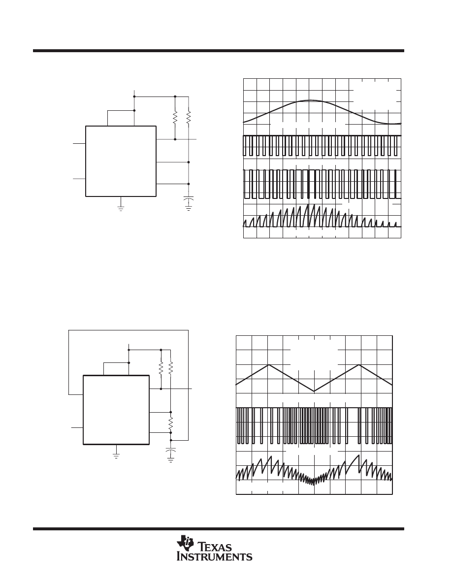
The operation of the timer can be modified by modulating the internal threshold and trigger voltages, which is
accomplished by applying an external voltage (or current) to CONT. Figure 18 shows a circuit for pulse-width
modulation. A continuous input pulse train triggers the monostable circuit, and a control signal modulates the
threshold voltage. Figure 19 shows the resulting output pulse-width modulation. While a sine-wave modulation
signal is shown, any wave shape could be used.
SLFS022E − SEPTEMBER 1973 − REVISED MARCH 2004
14
POST OFFICE BOX 655303
•
DALLAS, TEXAS 75265
APPLICATION INFORMATION
THRES
GND
C
RA
RL
VCC (5 V to 15 V)
Output
DISCH
OUT
VCC
RESET
TRIG
CONT
Modulation
Input
(see Note A)
Clock
Input
NOTE A: The modulating signal can be direct or capacitively coupled
to CONT. For direct coupling, the effects of modulation
source voltage and impedance on the bias of the timer
should be considered.
4
8
3
7
6
2
5
Pin numbers shown are for the D, JG, P, PS, and PW packages.
1
Figure 18. Circuit for Pulse-Width Modulation
V
oltage − 2 V/div
Time − 0.5 ms/div
ÏÏÏÏÏÏ
Capacitor Voltage
ÏÏÏÏÏ
ÏÏÏÏÏ
Output Voltage
ÏÏÏÏÏÏ
ÏÏÏÏÏÏ
Clock Input Voltage
ÏÏÏÏ
ÏÏÏÏ
ÏÏÏÏ
RA = 3 k
Ω
C = 0.02
µ
F
RL = 1 k
Ω
See Figure 18
ÏÏÏÏÏÏÏÏ
ÏÏÏÏÏÏÏÏ
Modulation Input Voltage
Figure 19. Pulse-Width-Modulation Waveforms
pulse-position modulation
As shown in Figure 20, any of these timers can be used as a pulse-position modulator. This application
modulates the threshold voltage and, thereby, the time delay, of a free-running oscillator. Figure 21 shows a
triangular-wave modulation signal for such a circuit; however, any wave shape could be used.
RB
Modulation
Input
(see Note A)
CONT
TRIG
RESET
VCC
OUT
DISCH
VCC (5 V to 15 V)
RL
RA
C
GND
THRES
NOTE A: The modulating signal can be direct or capacitively coupled
to CONT. For direct coupling, the effects of modulation
source voltage and impedance on the bias of the timer
should be considered.
Pin numbers shown are for the D, JG, P, PS, and PW packages.
4
8
3
7
6
2
5
Output
Figure 20. Circuit for Pulse-Position Modulation
Figure 21. Pulse-Position-Modulation Waveforms
V
oltage − 2 V/div
ÏÏÏÏÏ
ÏÏÏÏÏ
ÏÏÏÏÏ
ÏÏÏÏÏ
RA = 3 k
Ω
RB = 500
Ω
RL = 1 k
Ω
See Figure 20
ÏÏÏÏÏÏ
ÏÏÏÏÏÏ
Capacitor Voltage
ÏÏÏÏÏ
ÏÏÏÏÏ
Output Voltage
ÏÏÏÏÏÏÏÏ
ÏÏÏÏÏÏÏÏ
Modulation Input Voltage
Time − 0.1 ms/div
SLFS022E − SEPTEMBER 1973 − REVISED MARCH 2004
15
POST OFFICE BOX 655303
•
DALLAS, TEXAS 75265
APPLICATION INFORMATION
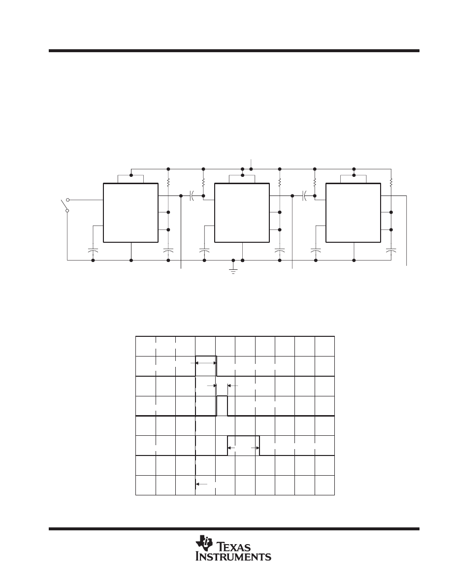
sequential timer
Many applications, such as computers, require signals for initializing conditions during start-up. Other
applications, such as test equipment, require activation of test signals in sequence. These timing circuits can
be connected to provide such sequential control. The timers can be used in various combinations of astable
or monostable circuit connections, with or without modulation, for extremely flexible waveform control. Figure 22
shows a sequencer circuit with possible applications in many systems, and Figure 23 shows the output
waveforms.
S
VCC
RESET
VCC
OUT
DISCH
GND
CONT
TRIG
4
8
3
7
6
1
5
2
THRES
RC
CC
0.01
CC = 14.7
µ
F
RC = 100 k
Ω
Output C
RESET
VCC
OUT
DISCH
GND
CONT
TRIG
4
8
3
7
6
1
5
2
THRES
RB 33 k
Ω
0.001
0.01
µ
F
CB = 4.7
µ
F
RB = 100 k
Ω
Output B
Output A
RA = 100 k
Ω
CA = 10
µ
F
µ
F
0.01
µ
F
0.001
33 k
Ω
RA
THRES
2
5
1
6
7
3
8
4
TRIG
CONT
GND
DISCH
OUT
VCC
RESET
µ
F
µ
F
CB
CA
Pin numbers shown are for the D, JG, P, PS, and PW packages.
NOTE A: S closes momentarily at t = 0.
Figure 22. Sequential Timer Circuit
V
oltage − 5 V/div
t − Time − 1 s/div
ÏÏÏÏÏ
See Figure 22
ÏÏÏÏ
Output A
ÏÏÏÏ
ÏÏÏÏ
Output B
ÏÏÏÏ
Output C
ÏÏ
ÏÏ
t = 0
ÏÏÏÏÏ
twC = 1.1 RCCC
ÏÏÏ
twC
ÏÏÏÏÏÏ
twB = 1.1 RBCB
ÏÏÏÏÏ
twA = 1.1 RACA
ÏÏ
ÏÏ
twA
ÏÏ
ÏÏ
twB
Figure 23. Sequential Timer Waveforms

PACKAGING INFORMATION
Orderable Device
Status
(1)
Package
Type
Package
Drawing
Pins Package
Qty
Eco Plan
(2)
Lead/Ball Finish
MSL Peak Temp
(3)
JM38510/10901BPA
ACTIVE
CDIP
JG
8
1
None
A42 SNPB
Level-NC-NC-NC
NE555D
ACTIVE
SOIC
D
8
75
Green (RoHS &
no Sb/Br)
CU NIPDAU
Level-1-260C-UNLIM
NE555DR
ACTIVE
SOIC
D
8
2500 Green (RoHS &
no Sb/Br)
CU NIPDAU
Level-1-260C-UNLIM
NE555P
ACTIVE
PDIP
P
8
50
Pb-Free
(RoHS)
CU NIPDAU
Level-NC-NC-NC
NE555PSLE
OBSOLETE
SO
PS
8
None
Call TI
Call TI
NE555PSR
ACTIVE
SO
PS
8
2000
Pb-Free
(RoHS)
CU NIPDAU
Level-2-260C-1 YEAR/
Level-1-235C-UNLIM
NE555PW
ACTIVE
TSSOP
PW
8
150
Pb-Free
(RoHS)
CU NIPDAU
Level-1-250C-UNLIM
NE555PWR
ACTIVE
TSSOP
PW
8
2000
Pb-Free
(RoHS)
CU NIPDAU
Level-1-250C-UNLIM
NE555Y
OBSOLETE
0
None
Call TI
Call TI
SA555D
ACTIVE
SOIC
D
8
75
Pb-Free
(RoHS)
CU NIPDAU
Level-2-260C-1 YEAR/
Level-1-235C-UNLIM
SA555DR
ACTIVE
SOIC
D
8
2500
Pb-Free
(RoHS)
CU NIPDAU
Level-2-260C-1 YEAR/
Level-1-235C-UNLIM
SA555P
ACTIVE
PDIP
P
8
50
Pb-Free
(RoHS)
CU NIPDAU
Level-NC-NC-NC
SE555D
ACTIVE
SOIC
D
8
75
None
CU NIPDAU
Level-1-220C-UNLIM
SE555DR
ACTIVE
SOIC
D
8
2500
None
CU NIPDAU
Level-1-220C-UNLIM
SE555FKB
ACTIVE
LCCC
FK
20
1
None
POST-PLATE
Level-NC-NC-NC
SE555JG
ACTIVE
CDIP
JG
8
1
None
A42 SNPB
Level-NC-NC-NC
SE555JGB
ACTIVE
CDIP
JG
8
1
None
A42 SNPB
Level-NC-NC-NC
SE555N
OBSOLETE
PDIP
N
8
None
Call TI
Call TI
SE555P
ACTIVE
PDIP
P
8
50
None
Call TI
Level-NC-NC-NC
(1)
The marketing status values are defined as follows:
ACTIVE: Product device recommended for new designs.
LIFEBUY: TI has announced that the device will be discontinued, and a lifetime-buy period is in effect.
NRND: Not recommended for new designs. Device is in production to support existing customers, but TI does not recommend using this part in
a new design.
PREVIEW: Device has been announced but is not in production. Samples may or may not be available.
OBSOLETE: TI has discontinued the production of the device.
(2)
Eco Plan - May not be currently available - please check
http://www.ti.com/productcontent
for the latest availability information and additional
product content details.
None: Not yet available Lead (Pb-Free).
Pb-Free (RoHS): TI's terms "Lead-Free" or "Pb-Free" mean semiconductor products that are compatible with the current RoHS requirements
for all 6 substances, including the requirement that lead not exceed 0.1% by weight in homogeneous materials. Where designed to be soldered
at high temperatures, TI Pb-Free products are suitable for use in specified lead-free processes.
Green (RoHS & no Sb/Br): TI defines "Green" to mean "Pb-Free" and in addition, uses package materials that do not contain halogens,
including bromine (Br) or antimony (Sb) above 0.1% of total product weight.
(3)
MSL, Peak Temp. -- The Moisture Sensitivity Level rating according to the JEDECindustry standard classifications, and peak solder
temperature.
Important Information and Disclaimer:The information provided on this page represents TI's knowledge and belief as of the date that it is
provided. TI bases its knowledge and belief on information provided by third parties, and makes no representation or warranty as to the
PACKAGE OPTION ADDENDUM
www.ti.com
18-Feb-2005
Addendum-Page 1

accuracy of such information. Efforts are underway to better integrate information from third parties. TI has taken and continues to take
reasonable steps to provide representative and accurate information but may not have conducted destructive testing or chemical analysis on
incoming materials and chemicals. TI and TI suppliers consider certain information to be proprietary, and thus CAS numbers and other limited
information may not be available for release.
In no event shall TI's liability arising out of such information exceed the total purchase price of the TI part(s) at issue in this document sold by TI
to Customer on an annual basis.
PACKAGE OPTION ADDENDUM
www.ti.com
18-Feb-2005
Addendum-Page 2
MECHANICAL DATA
MCER001A – JANUARY 1995 – REVISED JANUARY 1997
POST OFFICE BOX 655303
•
DALLAS, TEXAS 75265
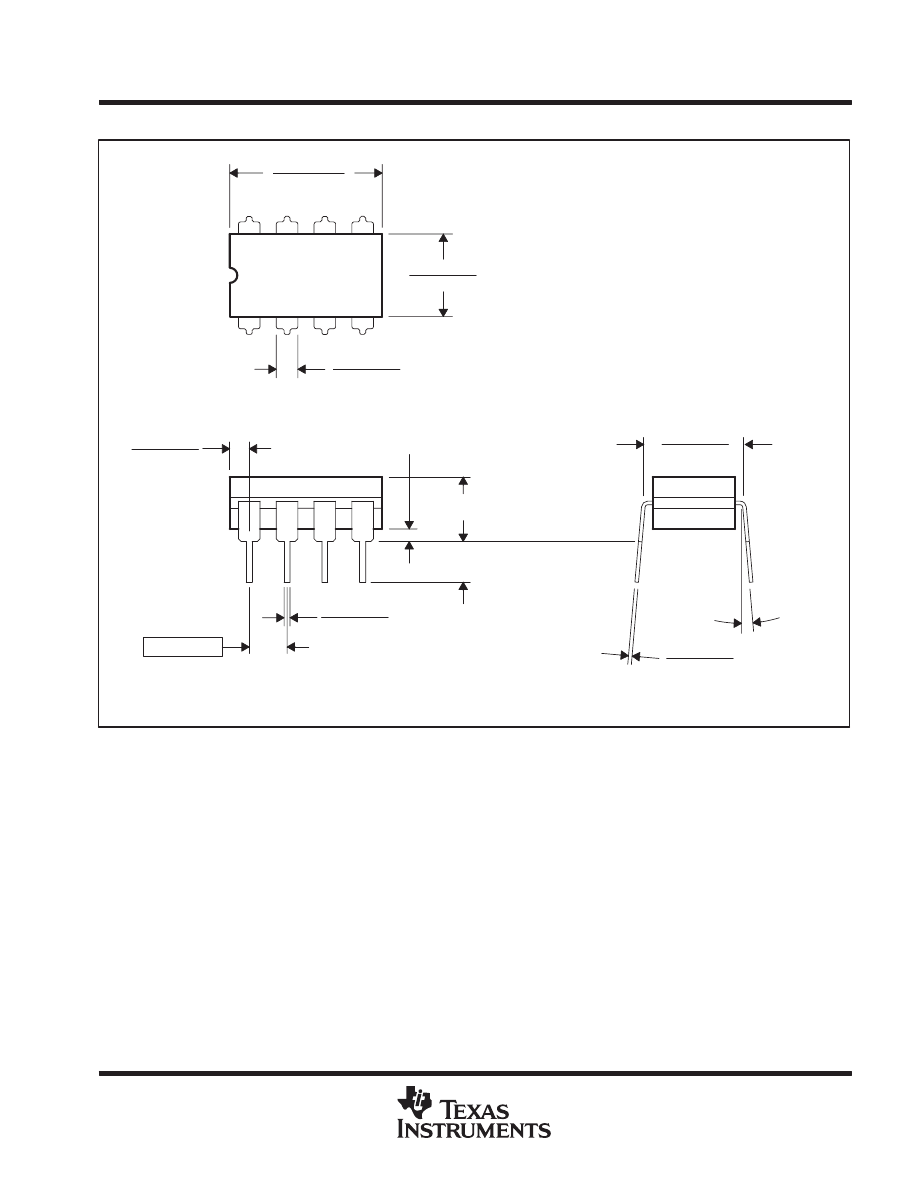
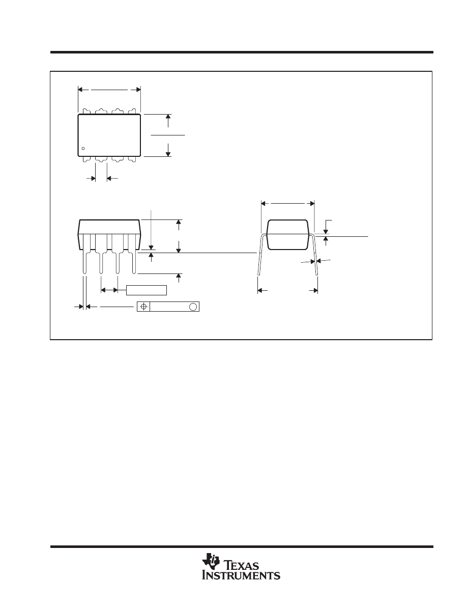
JG (R-GDIP-T8)
CERAMIC DUAL-IN-LINE
0.310 (7,87)
0.290 (7,37)
0.014 (0,36)
0.008 (0,20)
Seating Plane
4040107/C 08/96
5
4
0.065 (1,65)
0.045 (1,14)
8
1
0.020 (0,51) MIN
0.400 (10,16)
0.355 (9,00)
0.015 (0,38)
0.023 (0,58)
0.063 (1,60)
0.015 (0,38)
0.200 (5,08) MAX
0.130 (3,30) MIN
0.245 (6,22)
0.280 (7,11)
0.100 (2,54)
0
°
–15
°
NOTES: A. All linear dimensions are in inches (millimeters).
B. This drawing is subject to change without notice.
C. This package can be hermetically sealed with a ceramic lid using glass frit.
D. Index point is provided on cap for terminal identification.
E. Falls within MIL STD 1835 GDIP1-T8
MECHANICAL DATA
MLCC006B – OCTOBER 1996
POST OFFICE BOX 655303
•
DALLAS, TEXAS 75265
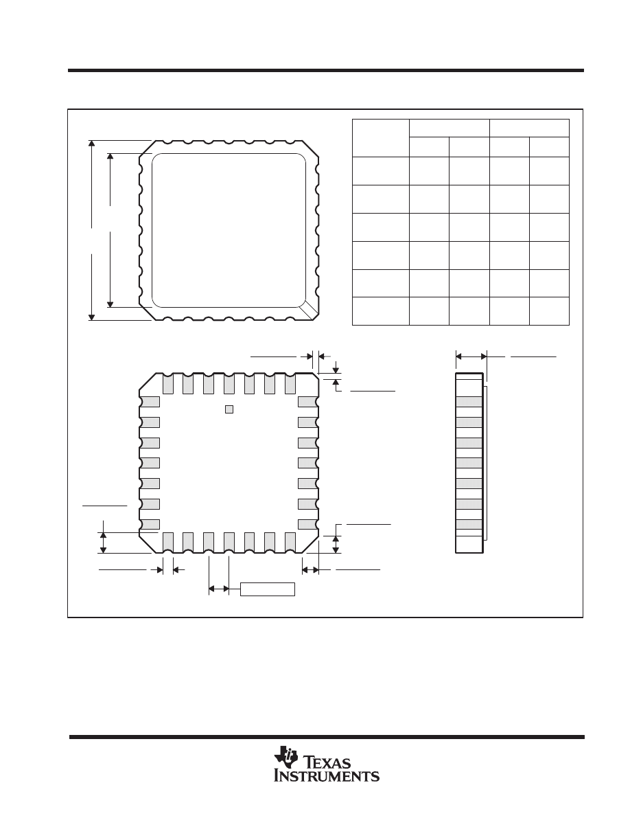
FK (S-CQCC-N**)
LEADLESS CERAMIC CHIP CARRIER
4040140 / D 10/96
28 TERMINAL SHOWN
B
0.358
(9,09)
MAX
(11,63)
0.560
(14,22)
0.560
0.458
0.858
(21,8)
1.063
(27,0)
(14,22)
A
NO. OF
MIN
MAX
0.358
0.660
0.761
0.458
0.342
(8,69)
MIN
(11,23)
(16,26)
0.640
0.739
0.442
(9,09)
(11,63)
(16,76)
0.962
1.165
(23,83)
0.938
(28,99)
1.141
(24,43)
(29,59)
(19,32)
(18,78)
**
20
28
52
44
68
84
0.020 (0,51)
TERMINALS
0.080 (2,03)
0.064 (1,63)
(7,80)
0.307
(10,31)
0.406
(12,58)
0.495
(12,58)
0.495
(21,6)
0.850
(26,6)
1.047
0.045 (1,14)
0.045 (1,14)
0.035 (0,89)
0.035 (0,89)
0.010 (0,25)
12
13
14
15
16
18
17
11
10
8
9
7
5
4
3
2
0.020 (0,51)
0.010 (0,25)
6
1
28
26
27
19
21
B SQ
A SQ
22
23
24
25
20
0.055 (1,40)
0.045 (1,14)
0.028 (0,71)
0.022 (0,54)
0.050 (1,27)
NOTES: A. All linear dimensions are in inches (millimeters).
B. This drawing is subject to change without notice.
C. This package can be hermetically sealed with a metal lid.
D. The terminals are gold plated.
E. Falls within JEDEC MS-004
MECHANICAL DATA
MPDI001A – JANUARY 1995 – REVISED JUNE 1999
POST OFFICE BOX 655303
•
DALLAS, TEXAS 75265
P (R-PDIP-T8)
PLASTIC DUAL-IN-LINE
8
4
0.015 (0,38)
Gage Plane
0.325 (8,26)
0.300 (7,62)
0.010 (0,25) NOM
MAX
0.430 (10,92)
4040082/D 05/98
0.200 (5,08) MAX
0.125 (3,18) MIN
5
0.355 (9,02)
0.020 (0,51) MIN
0.070 (1,78) MAX
0.240 (6,10)
0.260 (6,60)
0.400 (10,60)
1
0.015 (0,38)
0.021 (0,53)
Seating Plane
M
0.010 (0,25)
0.100 (2,54)
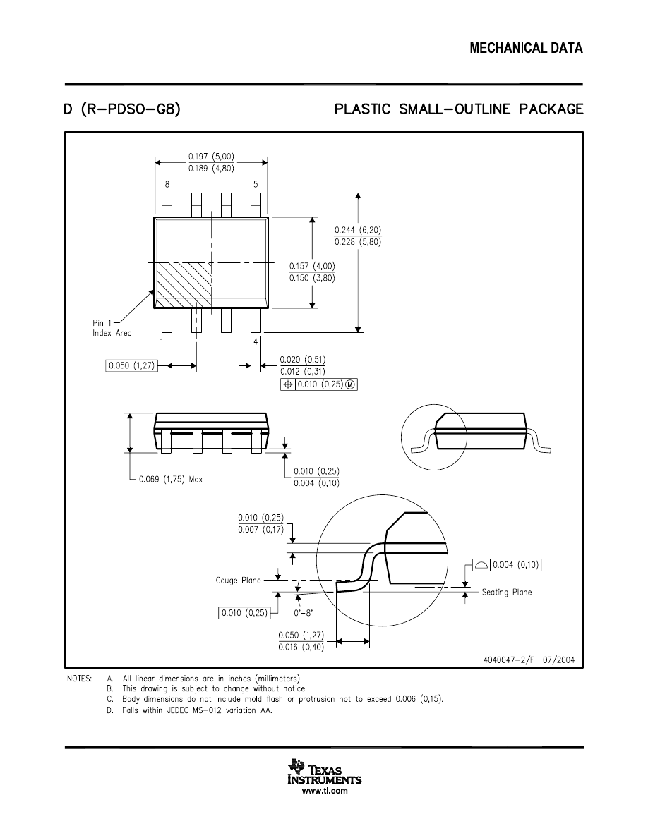
NOTES: A. All linear dimensions are in inches (millimeters).
B. This drawing is subject to change without notice.
C. Falls within JEDEC MS-001
For the latest package information, go to http://www.ti.com/sc/docs/package/pkg_info.htm
MECHANICAL DATA
MTSS001C – JANUARY 1995 – REVISED FEBRUARY 1999
POST OFFICE BOX 655303
•
DALLAS, TEXAS 75265
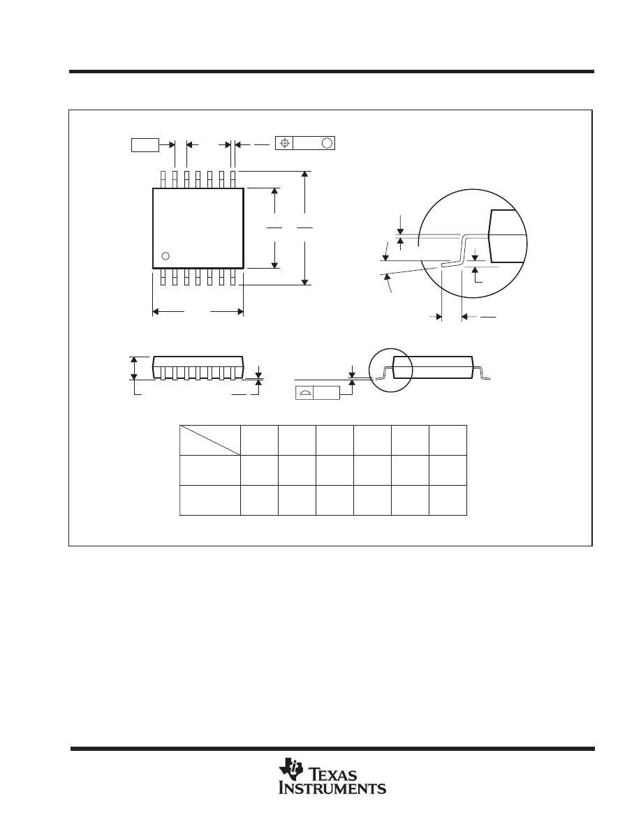
PW (R-PDSO-G**)
PLASTIC SMALL-OUTLINE PACKAGE
14 PINS SHOWN
0,65
M
0,10
0,10
0,25
0,50
0,75
0,15 NOM
Gage Plane
28
9,80
9,60
24
7,90
7,70
20
16
6,60
6,40
4040064/F 01/97
0,30
6,60
6,20
8
0,19
4,30
4,50
7
0,15
14
A
1
1,20 MAX
14
5,10
4,90
8
3,10
2,90
A MAX
A MIN
DIM
PINS **
0,05
4,90
5,10
Seating Plane
0
°
– 8
°
NOTES: A. All linear dimensions are in millimeters.
B. This drawing is subject to change without notice.
C. Body dimensions do not include mold flash or protrusion not to exceed 0,15.
D. Falls within JEDEC MO-153

IMPORTANT NOTICE
Texas Instruments Incorporated and its subsidiaries (TI) reserve the right to make corrections, modifications,
enhancements, improvements, and other changes to its products and services at any time and to discontinue
any product or service without notice. Customers should obtain the latest relevant information before placing
orders and should verify that such information is current and complete. All products are sold subject to TI’s terms
and conditions of sale supplied at the time of order acknowledgment.
TI warrants performance of its hardware products to the specifications applicable at the time of sale in
accordance with TI’s standard warranty. Testing and other quality control techniques are used to the extent TI
deems necessary to support this warranty. Except where mandated by government requirements, testing of all
parameters of each product is not necessarily performed.
TI assumes no liability for applications assistance or customer product design. Customers are responsible for
their products and applications using TI components. To minimize the risks associated with customer products
and applications, customers should provide adequate design and operating safeguards.
TI does not warrant or represent that any license, either express or implied, is granted under any TI patent right,
copyright, mask work right, or other TI intellectual property right relating to any combination, machine, or process
in which TI products or services are used. Information published by TI regarding third-party products or services
does not constitute a license from TI to use such products or services or a warranty or endorsement thereof.
Use of such information may require a license from a third party under the patents or other intellectual property
of the third party, or a license from TI under the patents or other intellectual property of TI.
Reproduction of information in TI data books or data sheets is permissible only if reproduction is without
alteration and is accompanied by all associated warranties, conditions, limitations, and notices. Reproduction
of this information with alteration is an unfair and deceptive business practice. TI is not responsible or liable for
such altered documentation.
Resale of TI products or services with statements different from or beyond the parameters stated by TI for that
product or service voids all express and any implied warranties for the associated TI product or service and
is an unfair and deceptive business practice. TI is not responsible or liable for any such statements.
Following are URLs where you can obtain information on other Texas Instruments products and application
solutions:
Products
Applications
Amplifiers
Audio
Data Converters
Automotive
DSP
Broadband
Interface
Digital Control
Logic
Military
Power Mgmt
Optical Networking
Microcontrollers
Security
Telephony
Video & Imaging
Wireless
Mailing Address:
Texas Instruments
Post Office Box 655303 Dallas, Texas 75265
Copyright
2005, Texas Instruments Incorporated

This datasheet has been download from:
Datasheets for electronics components.
Wyszukiwarka
Podobne podstrony:
NE555 Texas Instruments id 3161 Nieznany
4063 (Texas Instruments) id 384 Nieznany (2)
ma741 Texas Instruments id 2757 Nieznany
TLC5945 (Texas Instruments)
TLC5922 (Texas Instruments)
TLC5923 (Texas Instruments)
TLC548, TLC549 (Texas Instruments)
TLC5941 (Texas Instruments)
TLC5921 (Texas Instruments)
TLC5920 (Texas Instruments)
TI89 TI92 Symbolic Math Guide Texas Instruments (2001) WW
TLC7528 (Texas Instruments)
LMV358 Texas Instruments
TIP74 (Texas Instruments)
ICL7135, TLC7135 (Texas Instruments)
więcej podobnych podstron