regulate with shunt currents as low as 1
mA (at 1.24 V) and as high as 8 A (a 78-
dB dynamic range).
The circuits can be used anywhere a
power- zener diode function would be
utilized. Some typical applications are:
1) A high-current (up to 8 A) preci-
sion shunt-regulator (“power zener”).
2) A precise +3.3-V/8-A power supply
derived from regulated +5 V.
1
3) A precision, high-current voltage
clamp for overvoltage protection of dc
power supplies.
IDEAS FOR DESIGN
132
ELECTRONIC DESIGN • February 7, 2000
Robert N. Buono
Buono Consulting, 31 Upper Lakeview Ave., Ringwood, NJ 07456;
(973) 962-0553; fax (973) 962-0554; e-mail: bbengg@aol.com
High-Current, Low-Voltage
Shunt Regulator
CIRCLE 521
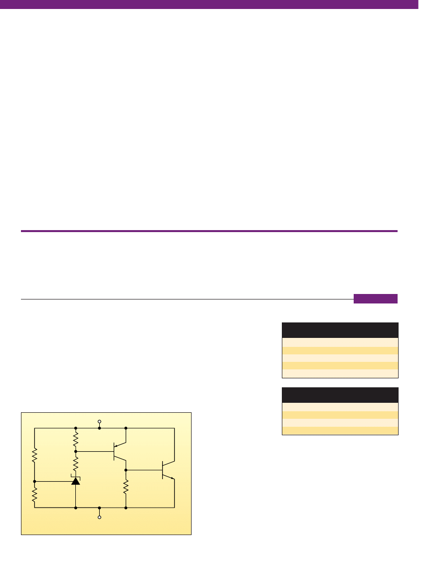
T
his design idea describes a high-
current (up to 8 A) shunt-regulator
built around the TLV431 low-volt-
age, adjustable, precision shunt-regula-
tor IC. Special attention was paid to
implementing this design as a “two-ter-
minal” circuit block, greatly increasing
the versatility of the design. The circuit
block can be conceptualized and imple-
mented in any application where a
power-zener diode would be used.
However, this circuit has much greater
precision, accuracy, and range of opera-
tional currents than such a diode.
Two circuit varieties are described,
based on the voltage range desired. For
shunt voltages ranging from 1.75 V to 6
V, the circuit in Figure 1 can be used; for
voltages between 1.24 V and 1.75 V, the
circuit of Figure 2 must be used.
Both circuits exploit
the best features of the
TLV431 shunt-regula-
tor—very low opera-
tional bias current levels
(80
µ
A max.), and a pre-
cision reference voltage
(1.24 V). These two fea-
tures allow the circuits to
regulate accurately over a
wide range of currents.
The circuit shown in Fig-
ure 1 will regulate pre-
cisely with shunt cur-
rents as low as 200
µ
A
and as high as 8 A. That’s
a 91.8-dB dynamic range.
The Figure 2 circuit will
1.
This high-current shunt-regulator is designed for applications
requiring shunt voltages ranging from 1.75 V to 6 V.
RA
1%
VREF
Q1
ZTX788B
RB
10k
1%
Q2
D44VH10
R1
1k
+
–
R3
1k
U1
TLV431C
TLV431AC
R2
100
All resistors are 1/8 W, 5%
except for RA and RB
V
SHUNT
R
B
(1%)
R
A
(1%)
1.24 V
OPEN
SHORT
1.50 V
10.0k
2.10k
1.70 V
10.0k
3.74k
TABLE 2: SUGGESTED
FIGURE 2 RESISTOR VALUES
V
SHUNT
R
B
(1%)
R
A
(1%)
R5 (1%)
1.75 V
10.0k
4.12k
100
2.00 V
10.0k
6.19k
100
2.50 V
10.0k
10.1k
100
5.00 V
10.0k
30.1k
100
TABLE 1: SUGGESTED
FIGURE 1 RESISTOR VALUES
The reason for the two different circuit
implementations (Figs. 1 and 2) is the
compliance voltage range of the cathode
terminal of the TLV431. The cathode ter-
minal can reach as high as 6 V, but can
only go approximately 200 mV below
the reference voltage (1.24 V) while
sinking current. For shunt voltages of
1.75 V up to 6 V, implemented using the
circuit of Figure 1, the cathode voltage
need only go as low as V
SHUNT
−
V
BE
. So
for V
SHUNT
= 1.75V, and V
BE
= 0.6V,
V
CATHODE
will be 1.15 V. This is within
the cathode’s operational voltage range.
Operation of the circuit in Figure 1 is
as follows: For voltages below the
shunt voltage, only the bias current of
the TLV431 will be drawn. The voltage
developed across R1, due to this bias
current, won’t be sufficient to turn on
Q1. Thus, Q1 and Q2 will be off. As
soon as the shunt voltage increases to
the point where V
REF
reaches 1.24 V
(defined by the resistive divider con-
sisting of R
A
and R
B
), the TLV431 will
begin to sink current at its cathode ter-
minal. This current will turn on Q1,
which in turn drives Q2. As a result, the
collector currents of both these transis-
tors are controlled by U1. The total
shunt current (I
SHUNT
)
∪
I
CATHODE
+
I
cQ1
+ I
cQ2
. Also, I
SHUNT
=
I
CATHODE
(
β
Q1)(
β
Q2). The high Beta (
β
= 400
min.) of Q1 makes a Darlington tran-
sistor unnecessary. It also allows lower
voltage operation, since the extra V
BE
drop of a Darlington is avoided.
For shunt voltages less than 1.75 V,
the circuit of Figure 2 should be used.
This circuit allows shunt voltages as low
as the reference voltage (1.24 V) to be
tightly regulated, with shunt currents
ranging from 1 mA up to 8 A. The main
difference between the two circuits is
that the current-mirror consisting of Q1
and Q2 allows Q3 and Q4 to be fully
driven with just a 150-mV range of cath-
ode voltage. Thus, the cathode voltage
of the TLV431 drops just 150 mV below
the reference voltage when regulating a
shunt voltage of 1.24 V.
Operation is as follows: For shunt
voltages below the set point, a bias cur-
rent will flow through Q1, R1, R2, and
R3. The bias current flowing through R2
creates an offset voltage that keeps Q2
off. This, in turn, keeps Q3 and Q4 off.
When the shunt voltage is high enough
so that V
REF
reaches 1.24 V (defined by
resistive divider R
A
and R
B
), U1 will start
to sink cathode current.
This cathode current will create a volt-
age drop across R1, causing Q1’s emitter
voltage to drop. The voltages on the
base and collector of Q1 will follow the
emitter. When the voltage at the collec-
tor of Q1 drops low enough, it will be-
gin to turn on Q2. Then Q3 and Q4 will
be driven just as Q1 and Q2 of Figure 1
were driven. (Note: Q3 and Q4 of Fig-
ure 2 are complementary devices to Q1
and Q2 of Figure 1). A drop across R1 of
150 mV maximum is sufficient to cause
8 A of shunt current to flow. Q2 of Fig-
ure 1 and Q4 of Figure 2 must have a
heat sink suitable for their level of
power dissipation, given by P
D
=
(I
SHUNT
)(V
SHUNT
).
Reference:
1. “Single IC in TO-220 Case Converts
5-V Rail to 3.3 V,”
ELECTRONIC DESIGN
, De-
cember 17, 1992, p. 37.
IDEAS FOR DESIGN
134
ELECTRONIC DESIGN • February 7, 2000
RA
1%
VREF
RB
10k
1%
R1
36
R2
68
R3
1k
R5
1k
+
–
U1
TLV431C
TLV431AC
All resistors are 1/8 W, 5%
except for RA and RB
R4
43
R6
1k
Q4
D45VH10
Q3
ZTX690B
Q1
2N3906
Q2
2N3906
1.70 V
3.3 V
1 mA min,
8 A max
+3.3 V @ 8 A
derived from +5.0 V
+
+
–
–
1 mA min
8 A max
VSHUNT
Precision shunt-regulator
or voltage clamp
5.0 V
+
–
VSHUNT
+
+
–
–
2.
When shunt voltages range from 1.24 V to 1.75 V, this circuit becomes a must.
3.
Shown are block-diagram representations of some possible design applications.
Wyszukiwarka
Podobne podstrony:
A Series Active Power Filter Based on a Sinusoidal Current Controlled Voltage Source Inverter
High Current Series Amplifiers id 201315
A Series Active Power Filter Based on Sinusoidal Current Controlled Voltage Source Inverter
Mike Holt Guide to Low Voltage Systems
A Series Active Power Filter Based on Sinusoidal Current Controlled Voltage Source Inverter
Home Power Magazine Extract Low Voltage Battery Disconnect
Build a Low Voltage Tube Hybrid Headphone Amp
Low Voltage Power Supply Circuits
[Ebook] Forex Optionetics High Profit Low Risk Trading
High Performance, Low Cost Photovoltaic Concentrator System
MCP16301 High Voltage Input Integrated Switch Step Down Regulator
Designing With Low Dropout Voltage Regulators
Induction Generator Based System Providing Regulated Voltage With Constant Frequency
dm7407 Hex Buffer Driver with High Voltage Open Collector Outputs
A Low Speed, High Torque, Direc Nieznany (2)
Ir2111 High Voltage High Speed Power Mosfet And Igbt Driver
więcej podobnych podstron