1 0 - 1
Chapter 10 FBs-PLC High-Speed Counter and Timer
10.1 FBs-PLC High-Speed Counter
The counting frequency of an ordinary PLC’s software counter can only reach tens of Hz (depending on the scan
time). If the frequency of input signal is higher than that, it is necessary to utilize high-speed counter (HSC), otherwise
loss count or even out of counting may occur. There are usually two types of HSC implemented for PLC. The hardware
high-speed counter (HHSC) employed special hardware circuit and the software high-speed counter (SHSC) which when
counting signal changes state will interrupt CPU to perform the increment/decrement counting operation. FBs-PLC
provides up to 4 HHSCs (in SoC chips) and 4 SHSCs. All of them are all 32-bit high speed counter.
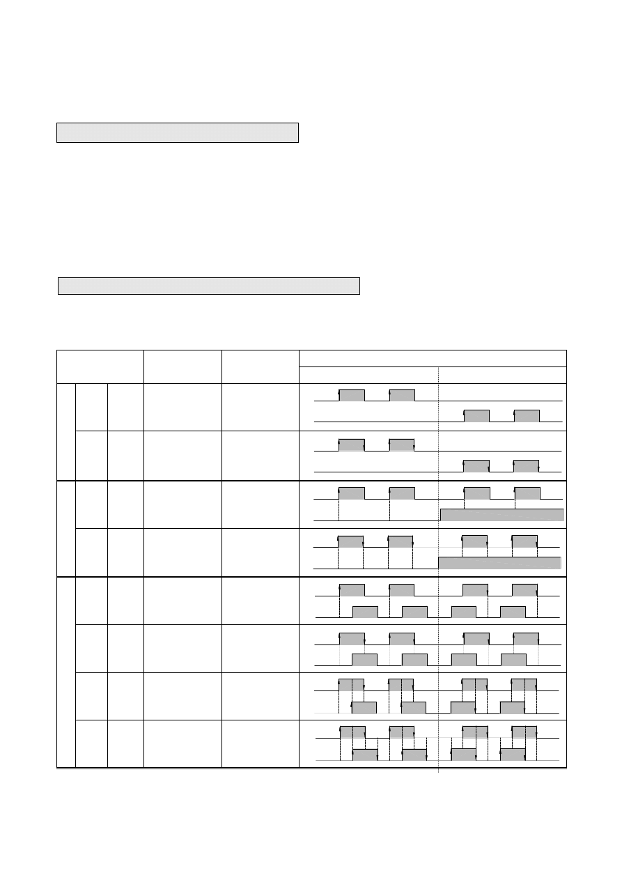
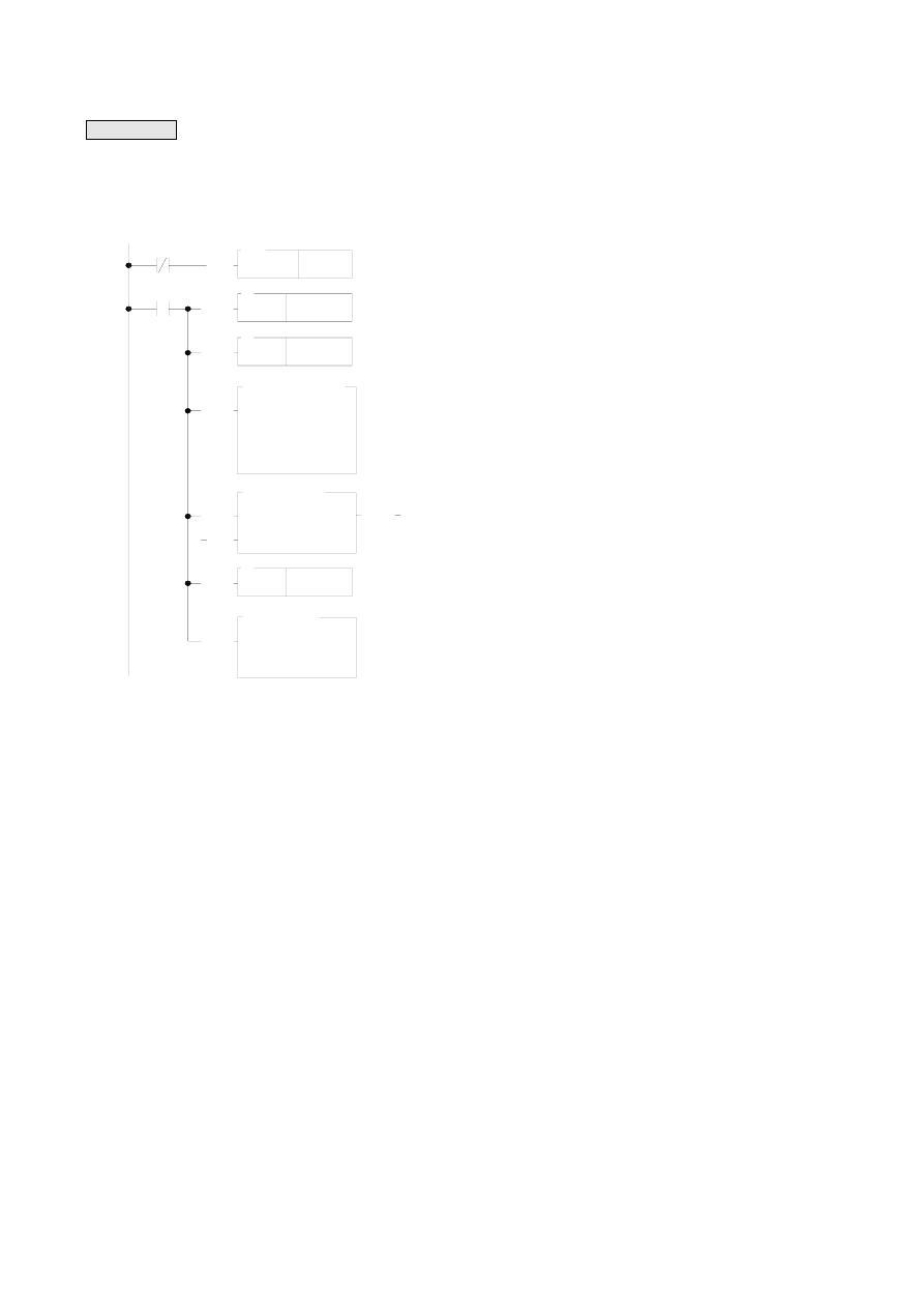
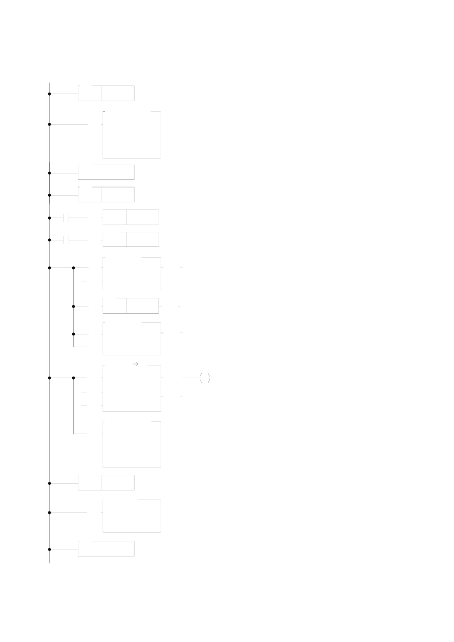
10.1.1 Counting Modes of FBs-PLC High-Speed Counter
As shown in the table below, each of the four FBs-PLC HHSCs and SHSCs provides 8 and 3, respectively, kind of
counting modes to choose from:
Counting Mode
HHSC
(HSC0~HSC3)
SHSC
(HSC4~HSC7)
Counting Waveform
Up Counting(+1)
Down Counting(
−1)
U
p
-d
ow
n
pu
ls
e
MD 0 U/D
○
○
U
D
MD 1 U/D
×2
○
U
D
Pu
ls
e
-di
re
cti
on
MD 2 P/R
○
○
R
P
MD 3 P/R
×2
○
R
P
AB phase
MD 4 A/B
○
○
B
A
MD 5 A/B
×2
○
A
B
MD 6 A/B
×3
○
A
B
MD 7 A/B
×4
○
A
B
• The up/down arrow (↑,↓) on the positive/negative edge in the waveform represents where counting (+1 or –1) occurs.
1 0 - 2
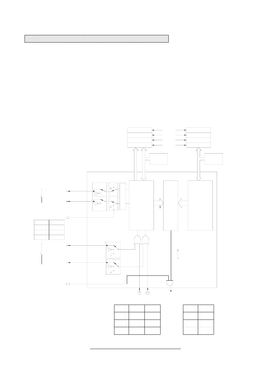
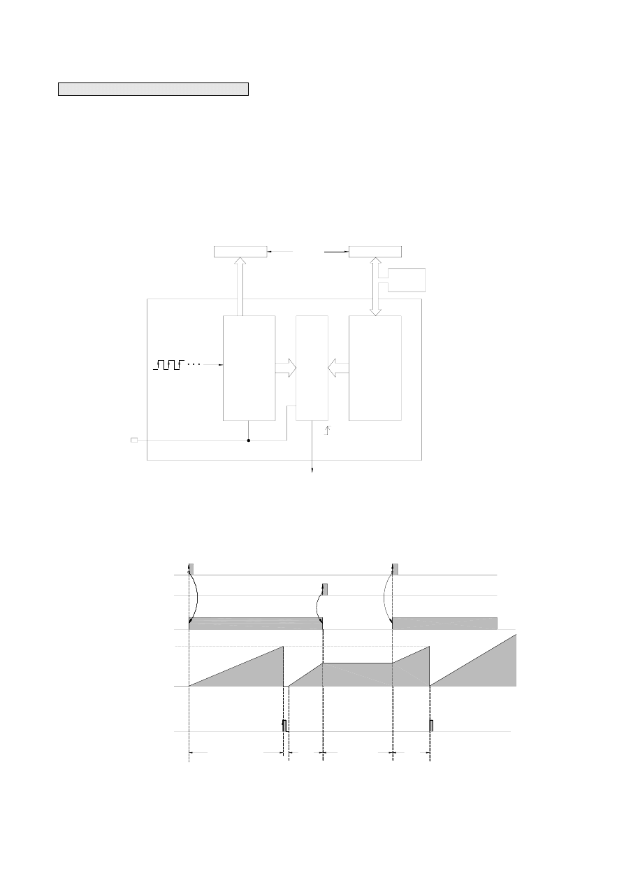
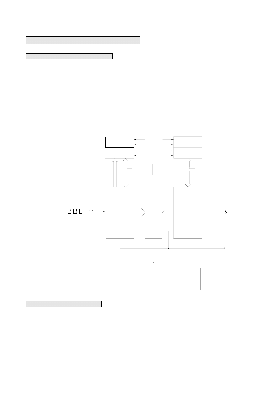
10.2 System Architecture of FBs-PLC High-Speed Counter
The diagrams below are the system architecture for FBs-PLC HHSC and SHSC where each one of them has
multi-purpose input and counting functions. Some of the functions are built-in (such as CV register number, PV register
number, interrupt label and relay number for software MASK, CLEAR and direction selection) that user need not to assign
for configuration. However, some functions, with a “*” marked in the diagrams below, must use the programming tool to
configure the HSC (such as HSC application selection, counting mode, application of each function input, inverse polarity
and appointment of corresponding input point number Xn) etc. For detailed structure and operation of the 8 kind of
counting modes that assigned in configuration, please refer to section 10.2.1~10.2.3 for explanation.
Note: CV (Current Value); PV (Preset Value).
CV Register
(CPU Intermal Memory)
PV Register
(CPU Internal Memory)
DR4096
DR4100
DR4104
DR4108
(HSC0)
(HSC1)
(HSC2)
(HSC3)
DR4098
DR4102
DR4106
DR4110
FUN92
(HSCTR)
FUN93
(HSCTW)
(SoC Chip)
CV
Register
(X0,X4,X8,X12)*
(X1,X5,X9,X13)*
D,R,B
(HSC0)
(HSC1)
(HSC2)
(HSC3)
M1942
M1948
M1978
M1981
0:UP
1:DN
(MD2,3 ONLY)
Counting
input
x1
x2
x3
x4
Software direction selection
M
C
Mask control
Clear control
Controlling
input
(X2,X6,X10,X14)*
(X3,X7,X11,X15)*
EN(FUN145)/
DIS(FUN146)
M
C
Com
parator
(HSC0)
(HSC1)
(HSC2)
(HSC3)
M1940
M1946
M1976
M1979
M1941
M1947
M1977
M1980
(HSC0)
(HSC1)
(HSC2)
(HSC3)
HSC0I
HSC1I
HSC2I
HSC3I
Software
Mask
Software
Clear
TO CPU
Interruput
Interrupt Mask
PV=CV
*
*
*
*
*
*
FUN93
(HSCTW)
PV
Register
U,P,A
System
Architecture
of HHSC(HSC0~HSC3)
z Use FUN92 to read out current counting value
from SoC chip hardware counter to put it into
CPU internal CV register.
z Use FUN93 to write CV register content to SoC
chip. Resets and updates the CV of hardware
counter in SoC chip.
z Use FUN93 to write
PV register of
hardware counter of
SoC chip.
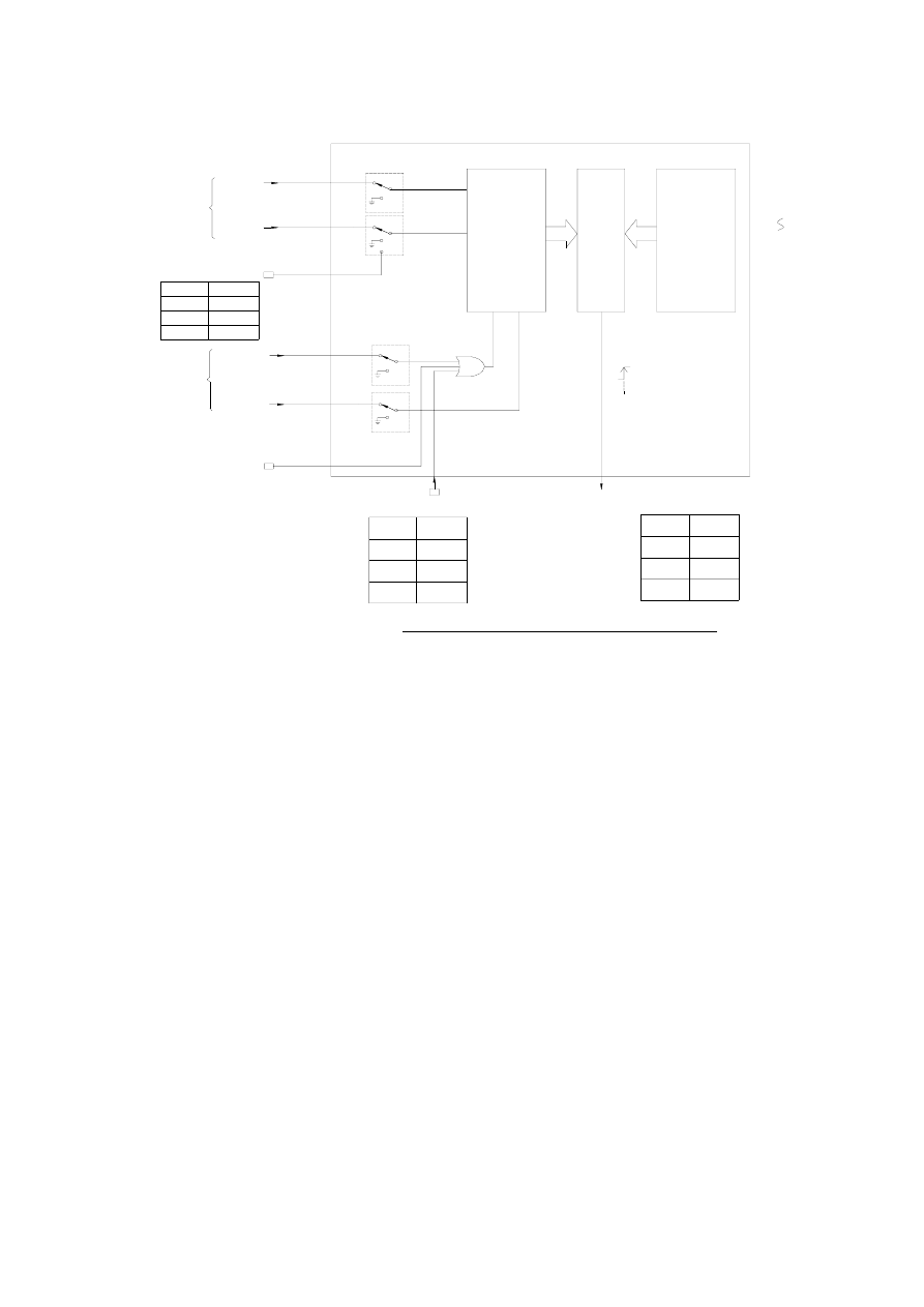
1 0 - 3
(
CPU Internal Memory)
PV Register
(X0~X15)*
(D,R,B)*
(HSC4)
(HSC5)
(HSC6)
(HSC7)
M1983
M1985
M1987
M 1989
0:UP
1:DN
(MD2 ONLY)
Counting
input
Software direction selection
M
C
Mask control
Clear control
Controlling
input
EN(FUN145)/
DIS(FUN146)
M
C
M 1982
M1984
M1986
M1988
HSC4I
HSC5I
HSC6I
HSC7I
Software Mask
Interrupt
Interrupt Mask
PV=CV
CV Register
DR4112(HSC4)
or
DR4116(HSC5)
or
DR4120(HSC6)
or
DR4124(HSC7)
(X0~X15)*
(X0~X15)*
(X0~X15)*
(HSC4)
(HSC5)
(HSC6)
(HSC7)
(HSC4)
(HSC5)
(HSC6)
(HSC7)
DR4114(HSC4)
or
DR4118(HSC5)
or
DR4122(HSC6)
or
DR4126(HSC7)
(HSC4)
(HSC7)
*
*
*
*
Co
mpar
ator
(U,P,A)*
System
Architecture
of SHSC(HSC4~HSC7)
z All control signals of HHSC and SHSC are default as Active High (i.e. Status =1 for active and 0 for non-active). In
order to cooperate with the sensor’s polarity, the HHSC counting inputs (U, D, P, R, A and B) and control inputs
(M and C) can be selected for polarity inverse.
z By default when the MASK control signal, M is 1, the HSC counting pulse will be masked without any counting
being performed and all HSC internal status (such as CV and PV) will remain unchanged. The HSC will function
normally only when M returns to “0”. Some sensors have Enable outputs which function is on the contrary to
MASK. Counters will not count when Enable = 0 and can only start functioning when Enable = 1. Then, function of
inverse polarity input of MASK can be selected to cooperate with the sensors having Enable output.
z When the CLEAR control signal, C is 1, the HSC internal CV register will be cleared to 0 and no counting will be
performed. The HSC will start counting from 0 when C returns to 0. Ladder program can also directly clear the CV
register (DR4112, DR4116, DR4120, and DR4124), so as to clear the current counting value to 0.
z The four sets of FBs-PLC HHSC are located in the SoC chips where the CV or the PV registers the user can’t
access directly. What the user can access are the CV registers (DR4096~DR4110) located in the CPU internal
memory. Ideally, the contents of CV and PV registers in the chips should be updated simultaneously with the CV
and PV registers in the CPU internal memory. However, to keep the correspondence between the two must be
loaded or read by the CPU when they, in fact, belong to two different hardware circuits. It is necessary to use
FUN93 to load the CV and the PV registers inside the CPU to the respective CV and PV registers (to allow HHSC
to start counting from this initial value. Then, FUN92 can be used to read back the counting value of the HHSC CV
register in the chips to the CV register in the CPU (i.e. the CV register in the CPU has the bi-direction function).
Since read can only be carried out when FUN92 is executed (so-called “sampling” reading), it might result in
difference between the HHSC CV value in the chips and the CV value in the CPU, the deviation will getting greater
especially when the counting frequency is high.

1 0 - 4
z When the counting frequency is not high or the demand for positioning precision is not so much, using FUN92 in
the main program to read the current counting value and then incorporate comparator instruction is adequate for a
simple counting positioning control.
z When the demand for positioning precision is higher, or in the multi-zone count setting control, it may use the
FUN92 to read the current counting value while in the time base interrupt routine and incorporate compare
instruction to perform more precise counting positioning control.
z As the demand for positioning precision is extremely high, it must use the preset interrupt function of hardware
counter. The preset value can load by FUN93 into the PV register of HHSC in the chipset. When CV value of
HHSC reaches this preset value, the hardware comparator in the HHSC will send interrupt to CPU at the very
moment CV=PV, and jump to interrupt subroutine to do real time control or procession.
z SHSC, on the other hand, uses the interrupt method to request an interrupt signal to the CPU when the counting
input is on the rising edge. Then, the CPU will determine whether it should decrease or increase the internal CV
register (since the CV register itself in the CPU is a SHSC CV register, no FUN92 or FUN93 is required). Each
time when CV is updated, if the CPU find that it is equal to the PV register value, the CPU will jump immediately to
the corresponding SHSC interrupt service routine for processing. Whenever there has a change in SHSC counting
or control input can cause the CPU to be interrupted. The higher the counting frequency, the more of CPU time
will be occupied. The CPU responding time will be considerably increased or even Watchdog time-out will be
caused to force the PLC to stop operating. Therefore, it is preferred to use HHSC first; if it needs to use SHSC, the
sum of all FBs-PLC SHSC input frequencies should not exceed 5KHz.
z None of the special relay controls, such as software MASK, CLEAR and direction control, is real time. This means
that although MASK, CLEAR or direction change has been set during routine scanning, the signal will only be
transmitted to HSC when I/O updating is under way after the completion of routine scanning. Hence, it is not
suitable for the real time control in HSC operation (which should be mainly used for initial setting before HSC
operation). Should real time control be required, please use hardware to control input or apply the FUN145(EN),
FUN146(DIS), FUN92(HSCTR), and FUN93(HSCTW) etc. instructions for control.
z Every HSC is equipped with the functions, ENable(FUN145) and DISable(FUN146), when SHSC is disabled, it will
stop counting and without the interrupt function ; when HHSC is disabled, the counting still works but the interrupt
function being disabled.
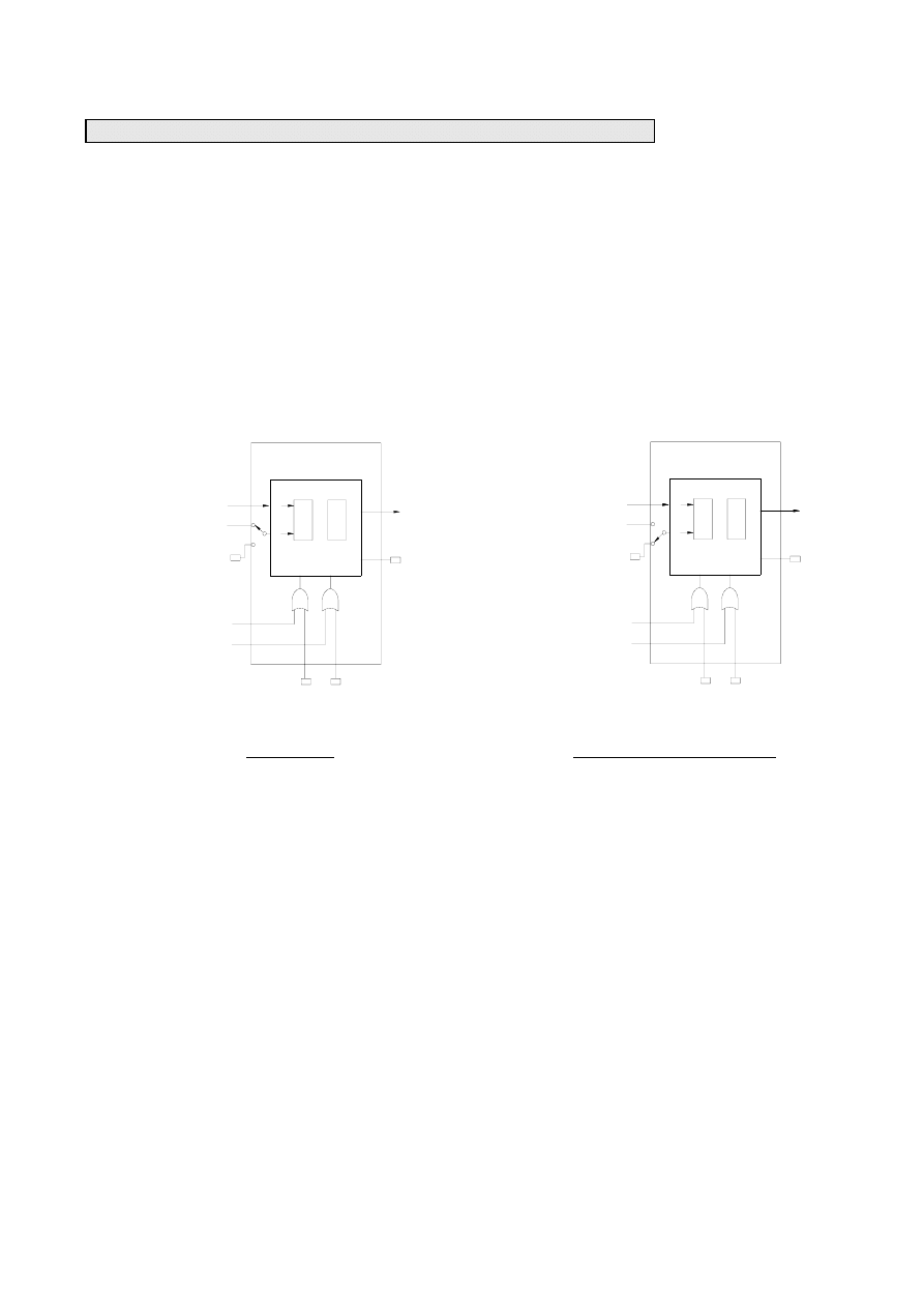
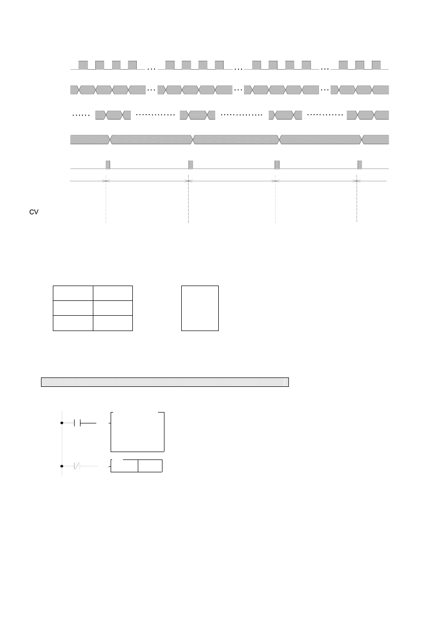
10.2.1 The Up/Down Pulse Input Mode of High-Speed Counter (MD0,MD1)
The up/down pulse input of high-speed counter has up counting pulse input (U) and down counting pulse input (D)
that are independent to each other without any phase relationship. Each of them will +1 (U) or –1 (D) on the CV value
when the rising edge of the pulse input occurs (both positive and negative edge for MD1). This also applies when the
rising (or falling) edge of the U and D pulse occur simultaneously (it will offset with each other). Both of the two modes
have the built-in software MASK and CLEAR (CLEAR is not available for SHSC) control functions, when the control
function are not in use should keep the status (such as M1940 and M1941) as “0”. Apart from the built-in software
MASK and CLEAR, the controls of hardware MASK and CLEAR can also be configured. The MASK control is first
performed by the OR operation of the hardware and software control, then the result is send to the HSC MASK control M,
and so does CLEAR. Taking HSC0 as an example, the function schematic diagrams for MD0 and MD1 configured
separately are shown as below.
1 0 - 5
HSC0
CV
PV
U
D
M
C
x1
EN/DIS
EN(FUN145)/
DIS(FUN146)
M1940 M1941
Up pulse X0
HSC0I
Interrupt
Down pulse X1
Hardware mask X2
Hardware clear X3
Software mask
Software clear
Down pulse X1
Hardware mask X2
Hardware clear X3
Software mask
Up pulse X0
PV
CV
Software clear
HSC0I
Interrupt
EN(FUN145)/
DIS(FUN146)
M1940 M1941
D
M
U
x2
EN/DIS
C
HSC0
MD0(U/D)
MD1(U/D
×2)(HHSC Only)
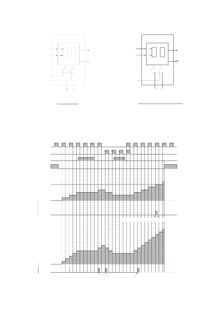
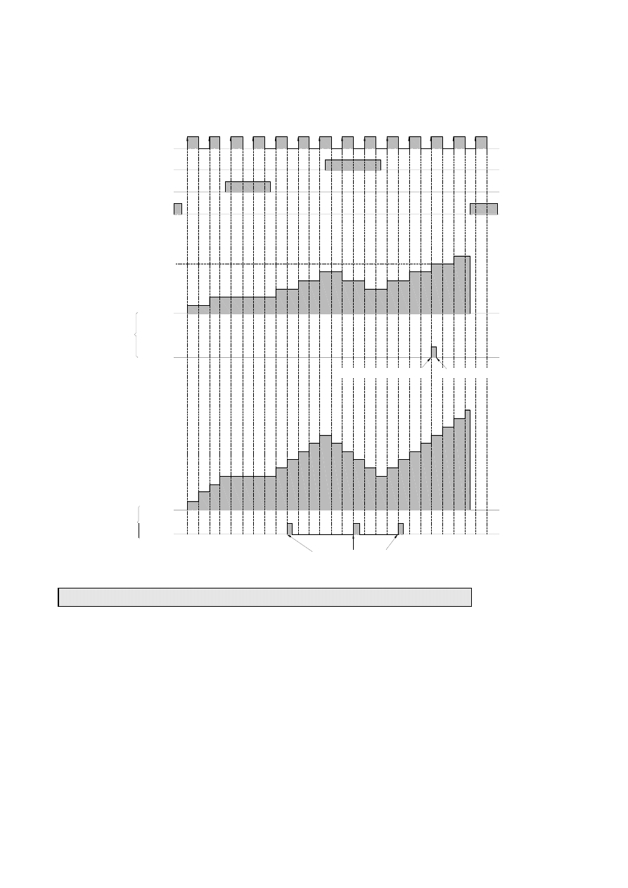
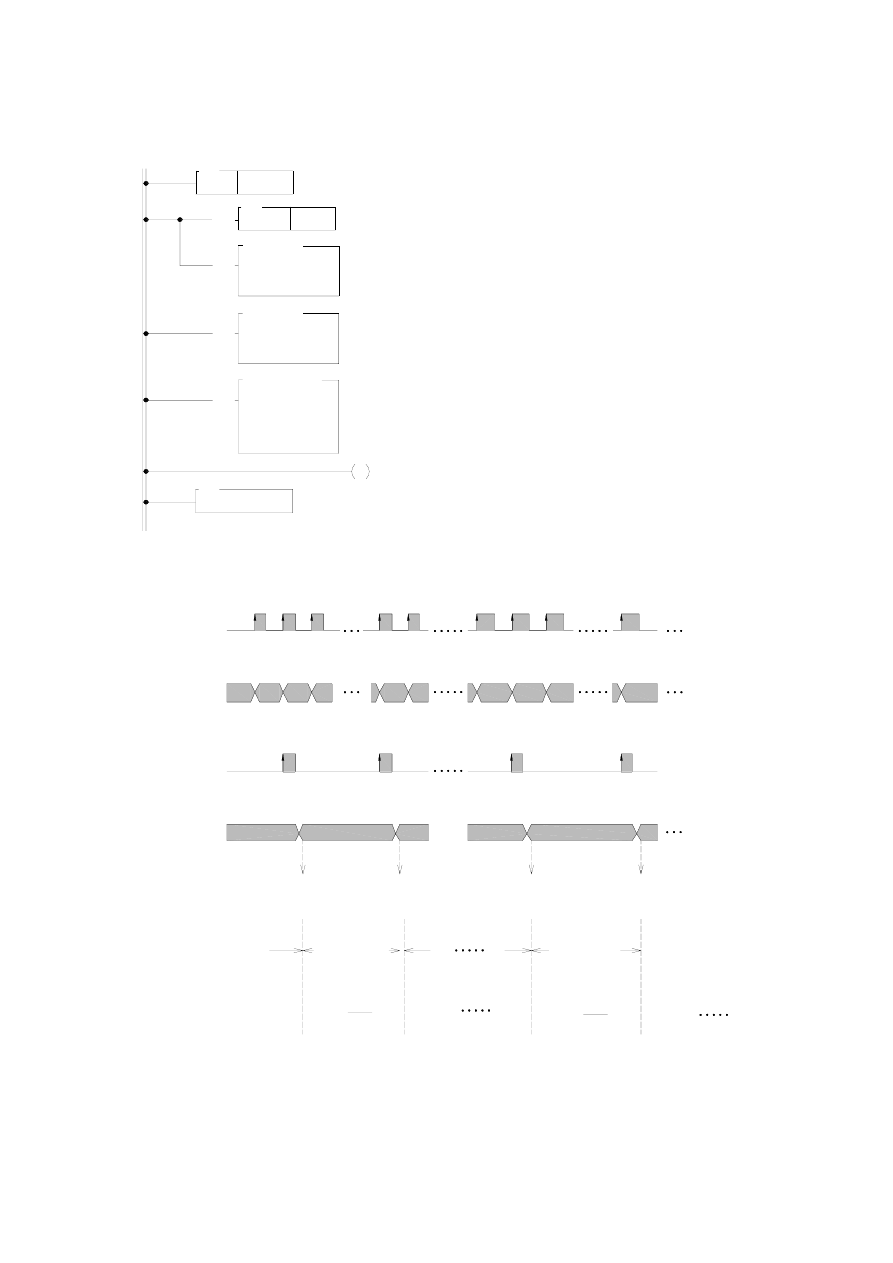
The Waveforms of the HSC, which is configured as up/down pulse input mode, and PV value is preset to 6:
X0(U)
X1(D)
M1940 or X2 (M)
M1941 or X3 (C)
PV=6
CV (x1)
HSC0I
MD0
CV (x2)
HSC0I
MD1
0
1
2
3
4
3
2
3
4
5
6
0
1
2
3
4
5
6
7
6
5
4
5
6
7
8
9
10
11
12
HSC0 sends interrupt to CPU CPU receives and handles this interrupt
HSC0 sends interrupt to CPU
1 0 - 6
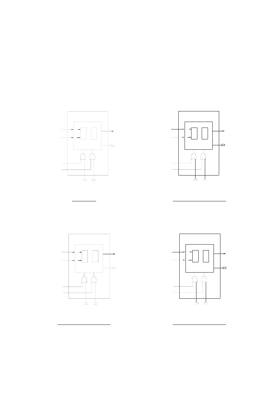
10.2.2 Pulse/Direction Input Mode of High-Speed Counter (MD2, MD3)
The pulse-direction input mode high-speed counter only has one counting pulse input P (pulse). It requires
another direction input R (Direction) to decide whether the CV value should +1 (R=0) or –1 (R=1) when the rising edge
(both rising and falling edges for MD3) of counting pulse arrives. The same applies to counting of MD2 and MD3 except
that MD2 only counts on the rising edge (+1 or –1) and MD3 counts on both rising and falling edges of PS pulse (twice the
counts of MD2). These two modes have built-in software MASK, software CLEAR (SHSC does not have clear). When
control function is not in use, it must keep the status (such as M1946 and M1947 in this example) to be 0. Apart from the
built-in software MASK and CLEAR, the controls of hardware MASK and CLEAR can also be configured. The MASK
control is first performed by the OR operation of the hardware and software control, then the result is send to the HSC
MASK control M, and so does CLEAR. The function schematic diagrams of HSC1 configured individually for MD2 and
MD3 are shown as below.
HSC1
Pulse input X4
Direction selecrion X5
CV
PV
P
R
M
C
x1
EN/DIS
Hardware mask X6
Hardware clear X7
Software mask
HSC1I
Interrupt
EN(FUN145)/
DIS(FUN146)
Software clear
M1946 M1947
HSC1
CV
PV
P
R
M
C
x2
EN/DIS
EN(FUN145)/
DIS(FUN146)
Software direction
selection
M1948
M1946 M1947
M1948
Pulse input X4
Hardware mask X6
Hardware clear X7
Software mask
HSC1I
Interrupt
Software clear
Software direction
selection
Direction selection X5
MD2(P/R)
MD3(P/R
×2)(HHSC Only)
Direction selection of MD2 and MD3 HHSC, for HSC or SHSC, can be come from the external inputs (such as X5 in
this example) or the special relay in CPU (such as M1948 in this example) to reduce the usage of external input points.
1 0 - 7
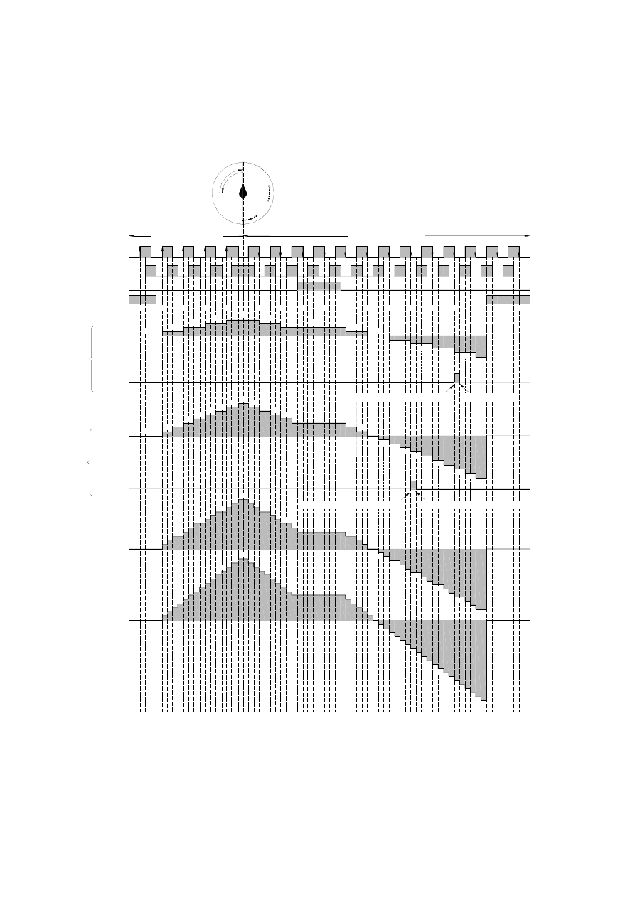
The diagram below is the waveform diagram for the relationship between counting and control of the two HSC. In
this example the PV value is to 6.
CV (x1)
HSC1I
MD2
CV (x2)
HSC1I
MD3
HSC1 sends interrupt to CPU
HSC1 sends interrupt to CPU
CPU receives and handles this interrupt
X6(M)
X7(C)
PV=6
1
2
3
4
4
5
5
5
6
7
8
9
8
7
6
6
7
8
9
10
11
12
1
2
3
4
4
5
5
3
4
6
7
0
X4(P)
X5(R)
10.2.3 AB Phase Input Mode of High-Speed Counter (MD4,MD5,MD6,MD7)
The AB phase high-speed counter is equipped with phase A and phase B pulse input with counting value +1 or –1,
depending on the phase relationship between the two, i.e. the related counting of the two phases. If phase A is ahead of
phase B, the CV value should be +1, else, the CV value should be –1. The counting of the four modes, MD4 (A/B), MD5
(A/B
×2), MD6 (A/B×3) and MD7 (A/B×4), of AB phase HSC are similar. Their differences are:
c
MD4 (A/B)
: The rising edge of A is +1 when A is ahead of B and the falling edge of A is –1 when A is behind B.
d
MD5 (A/B
×2) : The rising and falling edges of A are +1 when A is ahead of B, and –1 when A is behind B (twice the
counts of MD4).
e
MD6 (A/B
×3) : The rising and falling edges of A and rising edge of B are +1 when A is ahead of B. The rising and
falling edges of A and the falling edge of B are –1 when A is behind
B (three times the
counts of
MD4).
f
MD7 (A/B
×4) : The rising and falling edges of A and B are +1 when A is ahead of B and the rising and falling edges
of A and B are –1 when A is behind B (four times the counts of MD4).
1 0 - 8
Other MD4~MD7 HSC modes also have built-in software MASK, software CLEAR (SHSC does not have clear).
When control function is not in use, it must keep the status (such as M1946 and M1947 in this example) to be 0. Apart
from the built-in software MASK and CLEAR, the controls of hardware MASK and CLEAR can also be configured. The
MASK control is first performed by the OR operation of the hardware and software control, then the result is send to the
HSC MASK control M, and so does CLEAR
.
The function schematic diagrams of HSC2 for the four MD4~MD7 HSC
modes are shown as below.
HSC2
CV
PV
A
B
M
C
x1
EN/DIS
EN(FUN145)/
DIS(FUN146)
M1976 M1977
B phase pulse X9
A phase pulse X8
Hardware mask X0
Hardeare clear X11
Hardware clear
Software mask
HSC2I
Interrupt
A phase pulse X8
B phase pulse X9
Software mask
Hardware mask X0
Hardeare clear X11
PV
CV
HSC2I
Interrupt
Hardware clear
EN(FUN145)/
DIS(FUN146)
M1976 M1977
B
M
A
x2
EN/DIS
C
HSC2
MD4(A/B)
MD5(A/B
×2)(HHSC Only)
HSC2
CV
PV
A
B
M
C
x3
EN/DIS
EN(FUN145)/
DIS(FUN146)
M1976 M1977
Software mask
Hardeare clear X11
Hardware clear
B phase pulse X9
A phase pulse X8
HSC2I
Interrupt
Hardware mask X10
A phase pulse X8
B phase pulse X9
Hardware mask X10
Hardeare clear X11
Software mask
PV
CV
HSC2I
Interrupt
Hardware clear
EN(FUN145)/
DIS(FUN146)
M1976 M1977
B
M
A
x4
EN/DIS
C
HSC2
MD6(A/B
×3)(HHSC Only)
MD7(A/B
×4)(HHSC Only)
1 0 - 9
The diagram below is the waveform diagram for the relationship between counting and control of the four HSC modes in
this example when the PV value is set as at -4.
t
s
r
u v
q
p
o
m
n
w
x
y
ef
g
h
i
j
k
l
Rotary encoder
X8(A)
Down counting
(B phase ahead A phase)
Up counting
(A phase ahead B phase)
X9(B)
X10(M)
X11(C)
CV(x1)
PV=-4
HSC2I
MD4
CV(x2)
PV=-4
HSC2I
MD5
MD6:CV(x3)
MD7:CV(x4)
o
p
q
r
s
1
2
3
4
s
0
3
2
1
0
r
q
p
o
n
m
0
l
k
j
i
h
g
-1
-2
-3
-4
-5
CPU receives and handles this interrupt
HSC2 sends interrupt to CPU
0
0
0
0
0
0
-1
-2
-3
-4
-5
1
1
2
2
3
3
4
4
5
6
7
8
7
6
5
-6
-7
-8
-9
-10
CPU receives and handles this interrupt
HSC2 sends interrupt to CPU
1
2
3
4
5
6
1
2
3
6
9
9
12
-1
-2
-3
-6
-9
-12
-15
1
3
5
6
9
12
12
9
6
3
2
1
15
-1
-3
-6
-9
-12
-20
0
Retraced point
1 0 - 1 0
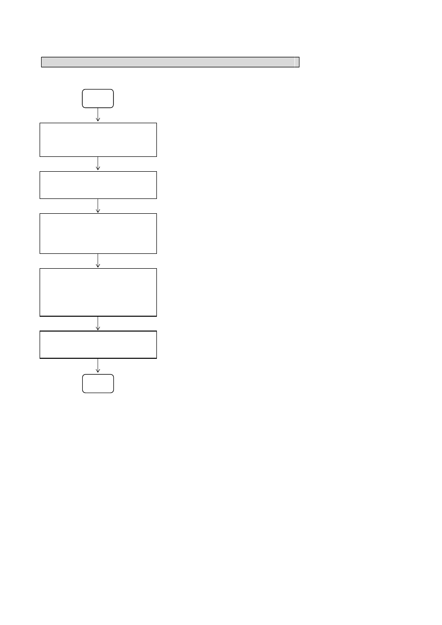
10.3 Procedure for FBs-PLC High-Speed Counter Application
Start
z Configure HSC counting mode and
respective input
(by FP-08 or WinProladder)
-------------
1. Please refer to Section 10.2 for respective HSC counting modes and
principles.
2. Please refer to Section 10.4 for setting examples.
z Complete hardware wiring
according to the previous input
assignment
-------------
1. Please refer to “Digital Input Circuit” in Chapter 6 “Hardware Manual”
for hardware wiring.
z Set HSC initial CV value and
interrupt PV value in the main
program
-------------
1. If the HSC is HHSC, it is necessary to apply FUN93 to load it into the
HHSC CV and PV in the SoC chip.
2. Please refer to Section 10.5 for program examples.
z Write necessary handling
procedures to be taken during
interrupt and condition for next
interrupt in sub program area
-------------
1. Please refer to Section 9.1 for subroutine structure.
2. Please refer to Section 10.5 “Actual Examples” for program
examples.
z Start the operation
-------------. Please refer to Section 10.5 for program examples and description.
End

1 0 - 1 1
10.4 HSC/HST Configuration
10.4.1 HSC/HST Configuration (Using FP-08)
The screen of FP-08 will be taken as an example to describe HSC Configuration in this section. The HSC
Configuration, in sequence, includes the following 5 items:
c
Select assignment for HSC/HST (only HHSC provides this item selection function). Proceed to next item if selection is
HSC. No other items are required if configured as HST.
d
Assign respective HSC counting modes (MD0~MD7). After keying in the mode number, FP-08 will automatically
display the HSC counting and control input names of the mode and reserve space for users to key in the external
input point number Xn. The blank mode field indicates the HSC is not in use.
e
Determine whether the respective counting inputs (U, D, P, R, A and B) and control inputs (M and C) are to be
applied or not (reserve the space if not in use and fill in the Xn value if it is to be applied. As respective Xn input
values of HHSC are fixed, it requires only to key in alphabet “X” and FP-08 will automatically make up the preset
number n).
f
Select whether the polarity of each HHSC counting input (U, D, P, R, A and B) is inverse or not, so as to match the
polarity of the encoder (0: Not inverse, 1: Inverse. Preset as 0).
g
Select whether the polarity of each HHSC control input (M and C) is inverse or not, so as to match the polarity of the
encoder (0: Not inverse, 1: Inverse. Preset as 0).
1 0 - 1 2
Examples applying FP-08 to perform the above mentioned
c~g
configurations
【Key Operation】
【LCD Display】
a
b
y HSC0 is preset as HSC
y HSC1 is preset as HSC
y HSC1 is used as a high-speed counter
HST1
y HSC2 is preset as HSC
y HSC3 is preset as HSC
y MD field is blank indicating that HSC0 is not
in use
y There is no need to configured HSC1 as it
has been set to HST (No Display).
y MD field of HSC2 is blank indicating MD is
not in use
*
y After 7 is keyed in, the respective MD7
input names will be displayed and the
preset values for A and B (X8 and X9) will
be filled automatically
y If MASK is required, just key in X and it will
automatically fills number 10
C
1 0 - 1 3
【Key Operation】
【LCD Display】
*
b
y Key in 2 and the preset number of P will
be filled automatically
y Move the cursor to R and key in “X”, it
will immediately change to X13 and
change it to be hardware direction
control
y HSC4 is not in use
y HSC5 is not in use
y HSC6 is set as MD0 and respective
input names of MD0 SHSC will be
displayed automatically
y Assign X10 as the up counting pulse
“U” for HSC6
y Assign X2 as the down counting pulse
“D” for HSC6
y HSC7 is not in use
y All counting inputs of every
HHSC(HSC0~HSC3)are preset as
non-inverse
y All MASK controls of HHSC are preset
as non-inverse
y Change all MASK inputs of HHSC to
inverse (i.e. the MASK function
becomes ENable)
y All CLEAR controls of HHSC are preset
as non-inverse
y Complete configuration and return to
the initial screen display (HSC0/HST0
Item Selection)
z Input value modification can be made by directly key in the new value to overwrite. Use
key to delete any input
value, if required.
z A blank field (without any value input) indicates the application of the HSC or the input is not required.
z “pulse” in the previous example represents the “Counting Input”, i.e. U and D, P and R or A and B, of HHSC.
z “POLAR” represents “POLARITY”, i.e. selection of inverse or non-inverse.
C
1 0 - 1 4
z The input point for respective HHSC counting and control inputs are fixed. Therefore, in the “Configuration Examples”
of the previous example, it needs only to key in “X” for each HHSC input to indicate that the input is to be applied and
FP-08 or WinProladder will automatically make up the preset number for X, to which no change will be allowed. The
user may assign respective SHSC counting or control inputs between X0~X15 freely. Hence, it is necessary to key in
both the “X” and the number n for SHSC input point number to make it complete.
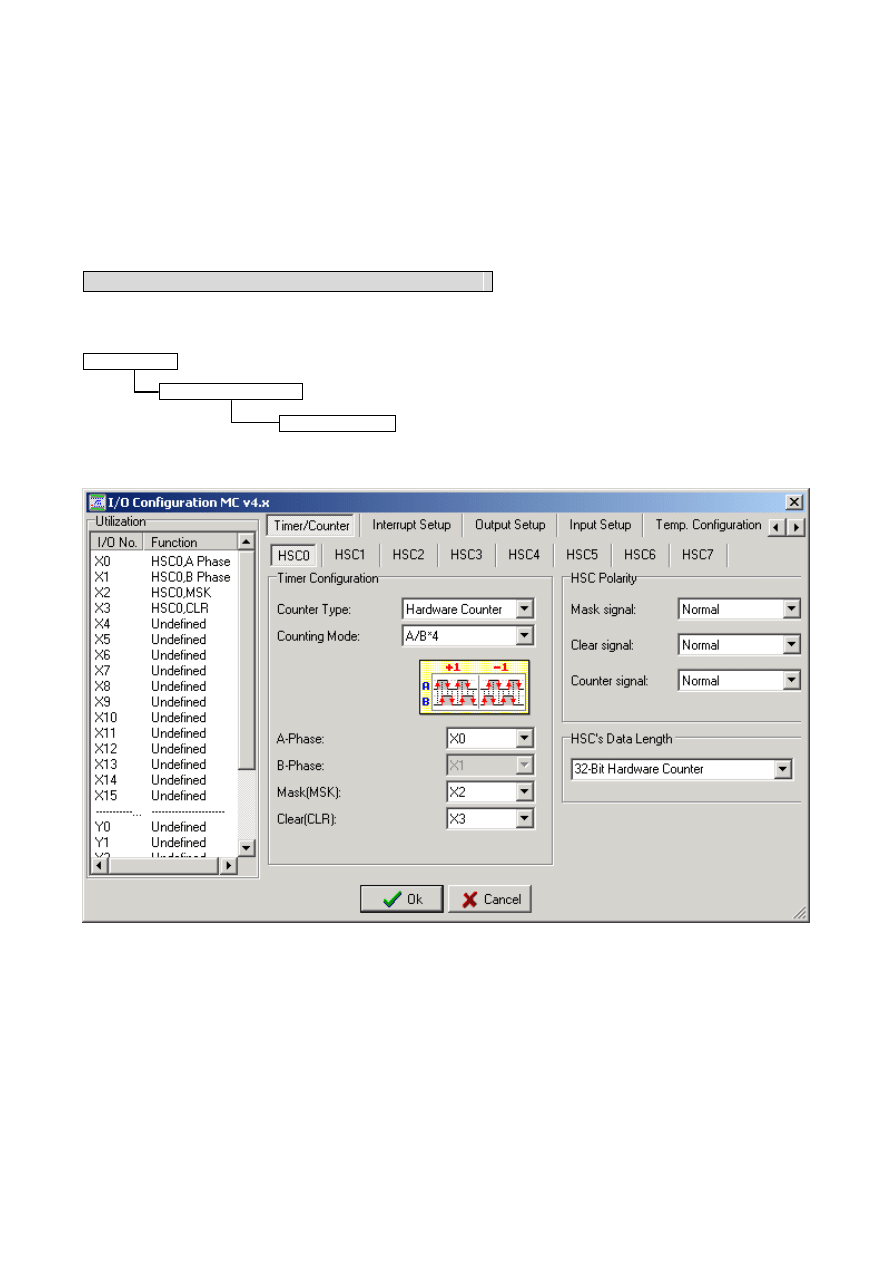
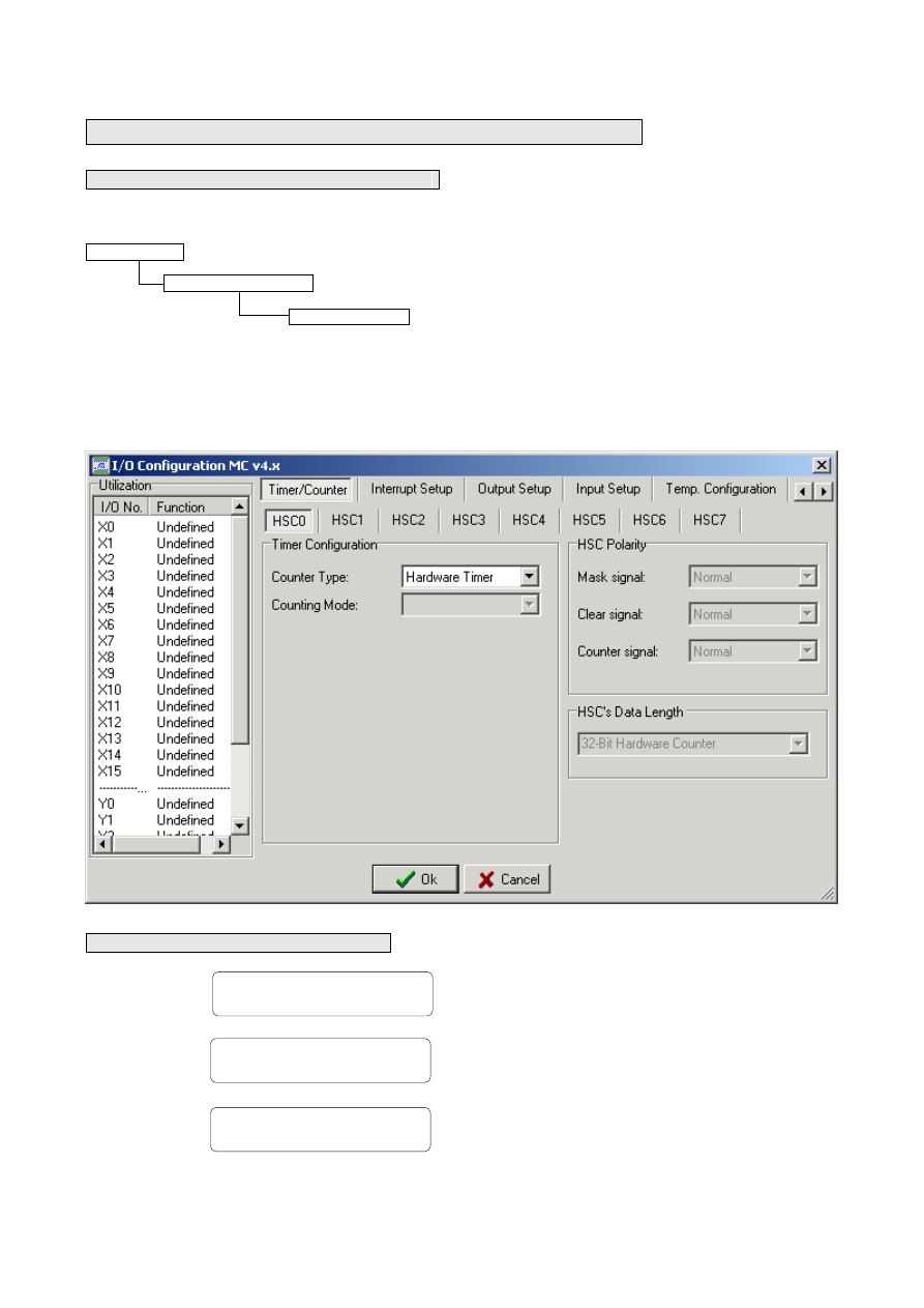
10.4.2 HSC/HST Configuration (Using WinProladder)
Click the item “I/O Configuration” which in Project Windows :
Project name
System Configuration
I/O Configuration
Æ Select “Timer/Counter”
When “Timer/Counter” window appear then you can choose the Timer or Counter which you want.
---《Timer/Counter Configuration》---
【 Counter Type 】: It can select Hardware Counter or Hardware Timer.
【 Counting Mode 】: It can select the Counting Mode( Example: U/D、P/R、A/B……)
【 A-Phase 】: Select the up pulse input signal. If the Mode is P/R Counting Mode ,and this item will be “PLS”; If the
Mode is U/D Counting Mode ,and this item will be “UP”.
【 B-Phase 】: Select the down pulse input signal. If the Mode is P/R Counting Mode ,and this item will be “DIR”; If the
Mode is U/D Counting Mode ,and this item will be “DN”.
【 Mask[MSK] 】: It can select Mask input.
1 0 - 1 5
【 Clear[CLR] 】: It can select Clear input.
---《HSC Polarity》area ---
【 Mask signal 】: Determining Mask signal is positive or negative.
【 Clear signal 】: Determining Clear signal is positive or negative.
【 Counter signal 】: Determining Counter signal is positive or negative.
---《HSC’s Data Length》area ---
It can choose 32-bit Hardware Counter mode or 16-bit Timer + 16-bit Counter mode. 32-bit Hardware Counter mode
means using two register to record the Counting value. The 16-bit Timer + 16-bit Counter mode means using one register
to record Counting value and the other register will be cyclic Timer.
All preset or selectable input point numbers, software MASK, software CLEAR, direction selection and other related
numbers of HHSC and SHSC are summarized in the table below:
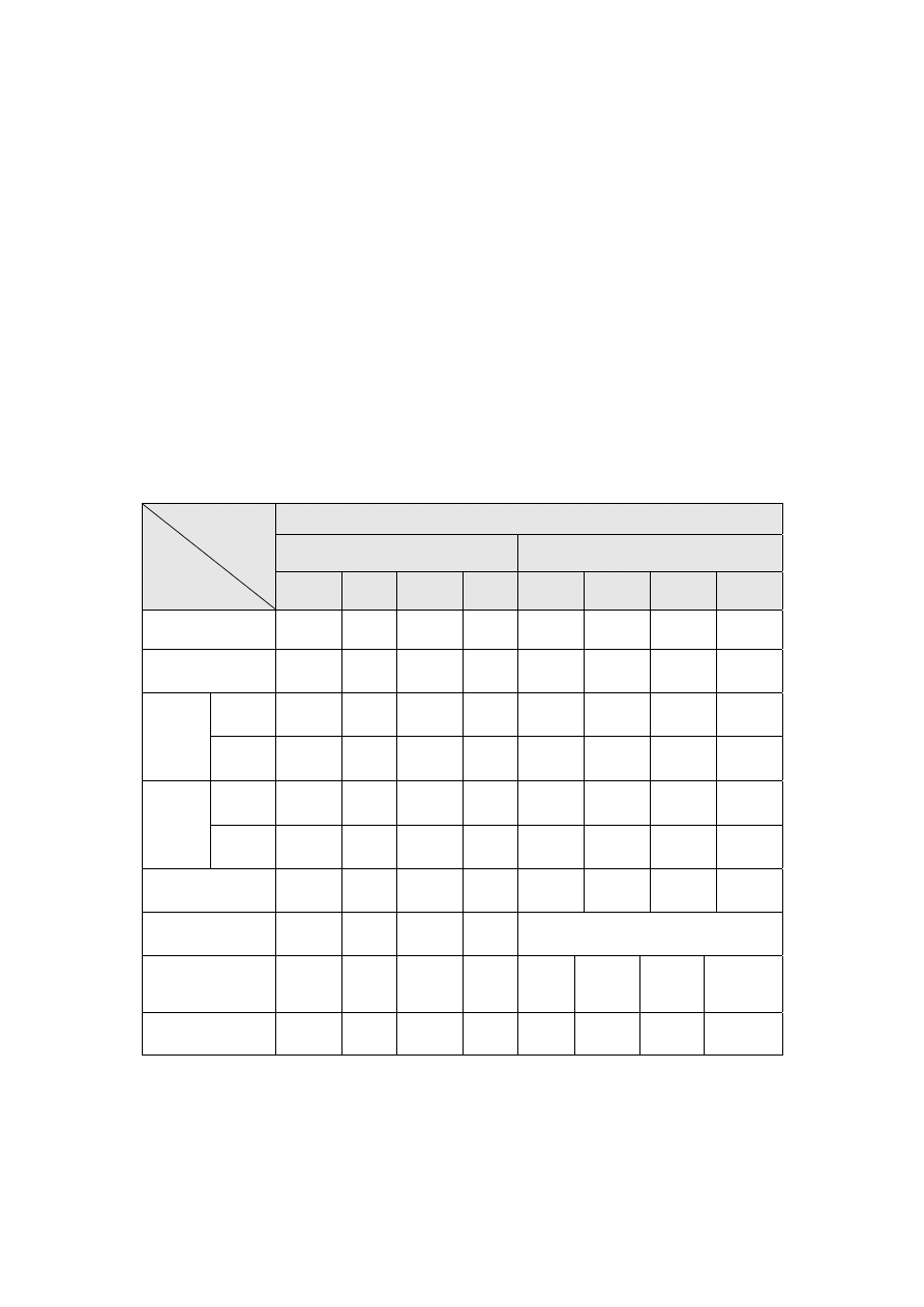
Type
Signal
Allowed
M A / M C / M N
HHSC
SHSC
HSC0
HSC1
HSC2
HSC3
HSC4
HSC5
HSC6
HSC7
CV Register
DR4096 DR4100 DR4104 DR4108 DR4112
DR4116
DR4120 DR4124
PV Register
DR4098 DR4102 DR4106 DR4110 DR4114
DR4118
DR4122 DR4126
Counting
Input
U,P or A
X0
X1/X4
X4/X5/X8 X5/X12
X0~X15
X0~X15
X0~X15 X0~X15
D,R or B
X1
X5
X9
X13
X0~X15* X0~X15* X0~X15* X0~X15*
Control
Input
Mask
X2
X6
X10
X14
X0~X15
X0~X15
X0~X15 X0~X15
Clear X3 X7 X11 X15
X0~X15
X0~X15
X0~X15 X0~X15
Software MASK
Relay
M1940 M1946
M1976
M1979
M1982
M1984
M1986 M1988
Software CLEAR
Relay
M1941 M1947
M1977
M1980
Clear the Current Value Register directly
Software Direction
Selection(MD2,3
Only)
M1942 M1948
M1978
M1981
M1983
M1985
M1987 M1989
Interrupt Subroutine
Label
HSC0I HSC1I
HSC2I
HSC3I
HSC4I
HSC5I
HSC6I HSC7I
* When SHSC works in MD2(P/R), direction chose by special relay M1983、M1985、M1987 and M1989.
z When working in A-B Mode(HHSC as MD4~MD7、SHSC as MD4), whose A/B input must be used in pair, as X8
and X9.(even number is A-Phase and odd number is B-Phase)
z The input point of X0~X15 in the table above can only be assigned once (i.e. used as one function), which can’t
repeat to be used.

1 0 - 1 6
z FB
s
-MN’s frequency can reach up to 460 KHz.( single phase and AB phase)
z FB
s
-MC’s frequency can reach up to 100 KHz. ( single phase and AB phase)
z FBs-MA’s frequency can reach up to 20KHz (single phase), and 10KHz (double phase).
z The total input frequencies of SHSC can’t be exceed 8 KHz; the higher the frequency, the more it occupy the system
(CPU) time, and the scanning duration will be extended abruptly.
z MA only support SHSC.
1 0 - 1 7
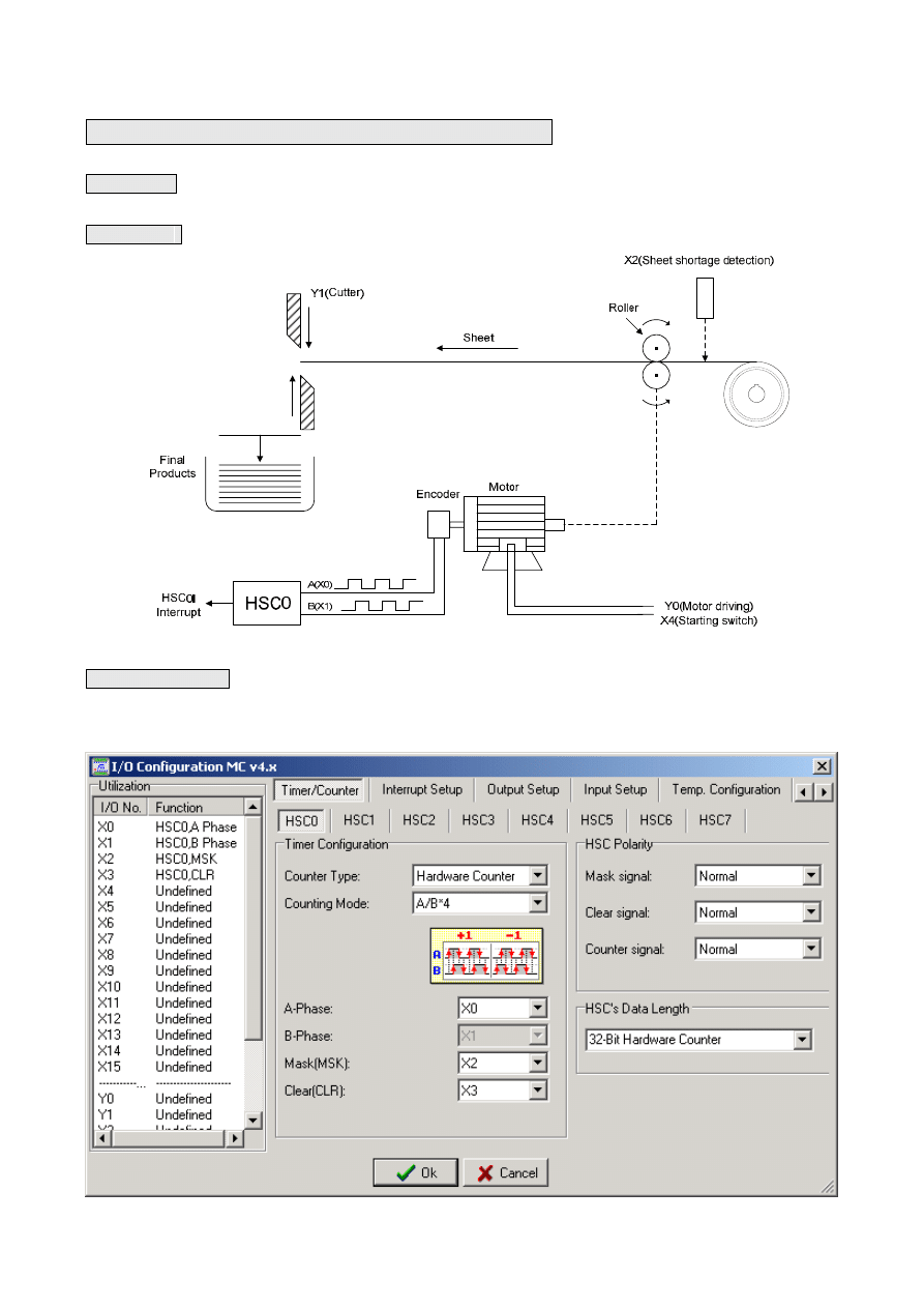
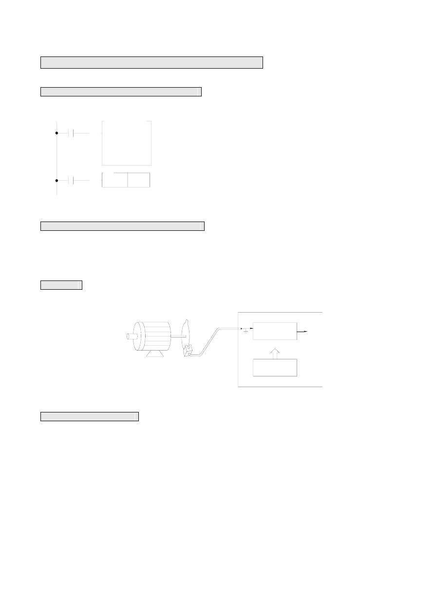
10.5 Examples for Application of High-Speed Counter
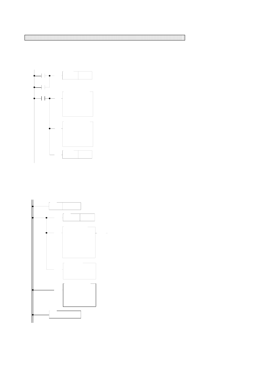
Example 1
This example uses high-speed counter for equal-length cutting control.
Mechanism
HSC configuration
(Just set HSC0 to MD7 and complete the configuration)
1 0 - 1 8
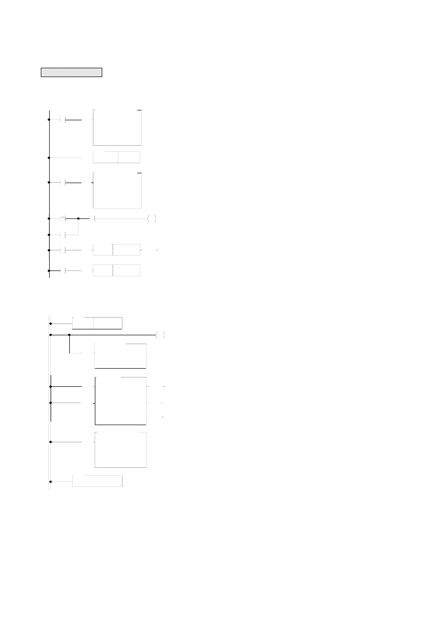
Control program
【Main Program】
EN
EN
EN
T0
Y1
Y0
X4
X4
X4
Y1
R ST
10
.01S
T0
X2
TUP
Y0
R0
HSC0
PV
H SC 0
S :
D :
C N:
H SCTR
92
CV
0
H SC 0
S :
C N:
D :
EN
EN
93DP.HSCTW
93DP.HSCTW
• Use FUN 93 to write the contents of the current value
register into the CV register of HSC0 in the SoC chip
CN =0 indicates HSC0
D
=0 indicates CV
• Use FUN 92 to read the counting value of the HSC0 CV
register in the SoC chip (store into DR4096)
• Store the counting of cutting length DR0 into DR4098 and
use FUN93 to store the value into the PV register of HSC0
in the SoC chip
CN =0 indicates HSC0
D
=1 indicates PV
• Start the motor
• Turn the cutter Y1 ON for 0.1 second
【Subroutine】
1 1 D .(+ )
7 4 .IM D I0
L B L
U /S
E N
E N
R 0
S b :
R 4 0 9 8
D :
B R
C Y
R 4 0 9 8
S a :
N :
D :
1
Y 1
D = 0
H S C 0 I
Y 1
6 5
6 9
R T I
9 3 D .H S C T W
C N :
D :
E N
S :
H S C 0
P V
R 4 0 9 8
• When HSC0 CV=PV in the SoC chip, the hardware will
automatically execute the interrupt subroutine labeled HSC0I
• When counting is up, turn Y1 ON (to cut materials)
• Output Y1 immediately to reduce the error caused by scan
time
• Calculate new cutting position and load HSC0 PV
【Description】
1. The main program will initialize the HSC0 CV (CV=0) in advance and move the cropping length (DR0) to the HSC0 PV
before starts Y0 to turn on the motor for material conveying.
2. When CV reaches PV, the length of R0 is added to the PV before being reloaded into HSC0 PV.
3. When all materials are rolled out, the material shortage detector X2 will be ON and stop the motor.
1 0 - 1 9
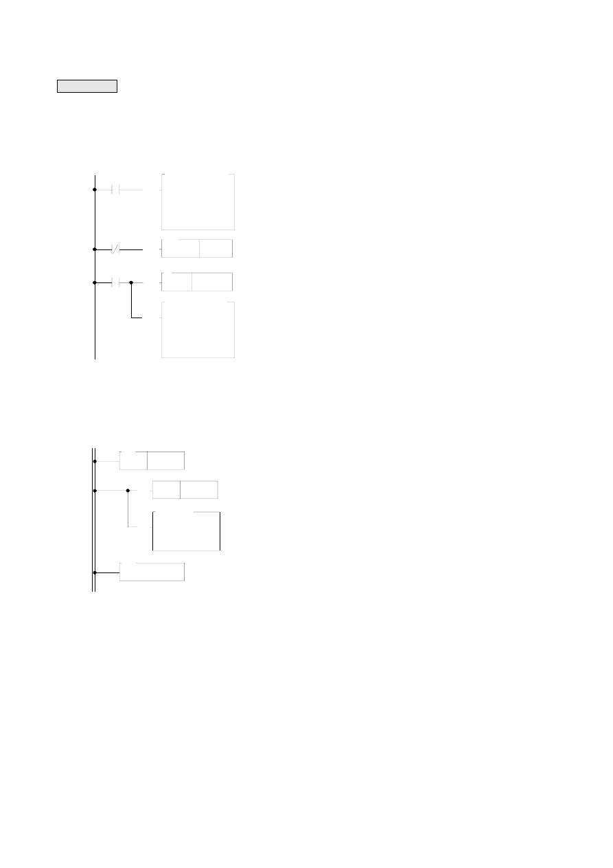
Example 2
Example of high speed counting up action processed by Interrupt
【Main Program】
M100
M101
M100
PV
D :
92
93DP.HSCTW
HSC0
HSC0
S :
CN:
EN
P
SET
HSCTR
EN
EN
R0
Y0
HSC0
93DP.HSCTW
S :
EN
CN:
D :
0
CV
•
Employ FUN93 to write the content of current value register into the
CV of HSC0 in SoC chip (reset)
CN =0,
represents
HSC0
D =0,
represents
CV
•
Employ FUN92 to read out the current counting value of HSC0
in SoC chip, and store it into the CV register (DR4096)
CN=0, represents HSC0
•
As M101 change from 0→1, start Y0 ON (begin to operate)
•
Employ FUN93 to write the content of preset register into HSC0 PV
in SoC chip, which serves as setting value of counting up interrupt
CN=0, represents HSC0
D
=1, represents PV
【Subroutine】
RTI
69
65
74.IMDI0
EN
D :
N :
EN RST
LBL
Y0
1
Y0
HSC0I
• Hardware high speed counter #0 interrupt label
• When time up, it sets Y0 OFF (stop)
• Let Y0 out immediately, so as to stop promptly
(otherwise Y0 will have a scan time output delay)
1 0 - 2 0
Example 3
Example of Immediate response of multi-zone high speed counting up by Interrupt Processing
【Main program】
M 101
X3
N :
8
S ET
D :
D :
N :
Y 8
Y8
8
Y8
E R R
R S T
M 110
H SC 1
R 200
C N :
D :
S :
PV
R 100
H SC 1
EN H SC TR
R S T
92
1/0
E N
E N
E N
E N
E N
E N
P
P
P
93D P .H SC TW
114P.Z-W R
74P.IM D I0
• Employ FUN92 to read out the current value of HSC1 in SoC
chip, and store it into current value register DR4100
CN =1, represents HSC1
• As M101 change from 0→1, clears the pointer register to 0
• Clears the flag of the last zone to be OFF
• Employ FUN93 to write preset register content into HSC1
PV in SoC chip, which serve as counting up setting value.
CN =1,
represents
HSC1
D =1,
represents
PV
• Clear Y8~Y15 to be OFF
• Set Y8 ON, it represents that it is at the zone 0 currently
• Set Y8~Y15 output t immediately
1 0 - 2 1
【Subroutine】
RTI
69
RST
66
D :
JMP
41.BITWR
15
(+1)
N :
D :
41.BITWR
N :
Ts :
Pr :
L :
S :
Rd :
93D.HSCTW
D :
N :
D :
74.IMDI0
CN:
101D.T R
LBL
EN
65
CLR
EN
INC
EN
INB
INB
EN
EN
M110
M110
EN
EN
EN
HSC1
110
Y8
8
PV
R4102
R4102
R100
R200
8
ERR
END
R100
R100
WY8
R100
ERR
OVF
110
WY8
Y15
ERR
X3+I
93D.HSCTW
D :
CN:
RTI
HSC1I
S :
EN
69
65
LBL
LBL
65
0
HSC1
CV
M110
• Label name for the X3 rising edge interrupt service
subroutine of X3+1
(it must assign X3 to be the rising edge interrupt input)
• When X3 changes from 0→1,employ FUN93 to write the
current register content to the HSC1 CV in SoC chip (reset).
CN = 1, represents HSC1
D = 1, represents CV
• Labeled as HSC1I hardware high speed counter interrupt
service subroutine.
• Turn Y15 OFF when the last zone finished.
• Make the previous zone output OFF
• Set the pointer point to the next zone
• Set the output of next zone to be ON
• Move the counting value of next zone (beginning from
DR200 pointer pointed register) to the preset register
DR4102
• When it’s the last zone, the M110 is ON
• Employ the FUN93 to write the preset value into the HSC1
PV in the SoC chip, which serves as counting up interrupt
setting point.
CN =1,
represents
HSC1
D =1,
represents
PV
• Y8~Y15 output transmitting immediately

1 0 - 2 2
10.6 FBs-PLC High-Speed Timer
The minimum timing unit (time base) of an ordinary PLC can only reach 1mS, on which the deviation in scan time
should also be added. Therefore, it is necessary to apply high-speed timer (HST) if a more precise timing (e.g. using timer
to cooperate with HSC for frequency measurement) is required.
FBs-PLC is built in a high-speed timer (HSTA) with a time base of 16-bits/0.1mS and, as described previously, four
32-bit high-speed counters (HSC0~HSC3) of HHSC that can work as the high speed timer (HST0~HST3) with a time
base of 32-bit/0.1mS for using. Thus, FBs-PLC can have up to five high-speed timers. As HSC and INT, all HST can be
enabled or disabled (default as enable) by the instructions EN (FUN145) and DIS (FUN146). HSTA and HST0~HST3 are
respectively described as below.
The finest time base for most of the ordinary PLC is 10mS. Though some PLC may have HST with a time base of
1mS. When deviations in the PLC scan time is taken into consideration (e.g. if the scan time is 10mS when the time base
is 1mS, the total deviation still exceeds 10mS), the figure of 1mS becomes meaningless. Therefore, these PLCs can’t be
applied in high precision timing. FBs-PLC, having a time base of 0.1mS, has no deviation in scan time for its time up is
sent out by interrupt to provide a precision 100 times better than ordinary PLCs’ timer application and can be used for
many applications demanding precision timing.
10.6.1 HSTA High-Speed Timer
HSTA is a 16-bit hardware timer built in the SoC chip. As HHSC, it must use the instruction FUN93 (HSCTW) to
load the PV to the HSTA PV in the chip, and with the instruction FUN92 (HSCTR) to read for CV. HSTA can be used as
a timer having two different functions. FBs-PLC will use it as a general 16-bit delay timer when PV
≥
2 and as a 32-bit
cyclic timer when PV=0.
1 0 - 2 3
A. HSTA 16-bit high-speed delay timer
(Timely interrupt timer)
After HSTA starts timing, the delay timer will delay for a time of PVx0.1mS before sending an interrupt out. When
PV>0, HSTA served as a delay timer which is 16-bit and its PV value can be set as 0002H~FFFFH. i.e. the delay time
can be set as 0.2mS~6.5535 seconds. Except that having a more precise time base and being able to send an interrupt
out immediately at time-up to provide a much higher timing precision, the applications of HSTA are the same as an
ordinary delay timer. The diagram below is the structure diagram for HSTA being used as a delay timer. Please refer to
Section 10.6.3 “Program Examples” for detailed function and application.
PV=CV
R4152
R4154
(HSTA)
CV Register
PV Register
FUN92
(HSCTR)
16 bit
16 bit
CV
PV
UP
0.1mS time base
EN(FUN145)/
DIS(FUN146)
Comparator
Interrupt label
HSTAI
EN/DIS
EN/DIS
FUN93
(HSCTW)
(SoC Chip)
EN(FUN145)
DIS(FUN146)
Timing/Non-timing
PV
CV
(R4152)
HSTAI
Td1
Non-timing
Td2
Td=Td1 + Td2
Td=0.1mS x PV
z Apply FUN93 to write the
PV into preset register of
HSTA high speed timer in
SoC chip, which serves as
timely interrupt timer (for
every set point of timer it
perform once the timely
interrupt subroutine with
label name of “HSTAI”).
PV
2
≧
1 0 - 2 4
B. HSTA 32-bit high-speed cyclic timer
The so-called “Cyclic Timer” is a timer that add 1 to its current value for every fixed interval and will persistently
carry out up counting cyclic timing. Its CV value will cycle around as 0, 1, 2, … 2147483647, 2147483648,
2147483649, …… 4294967295, 0, 1, 2, … (as the time base is 0.1mS, CV value x 0.1mS will be its accumulative time). In
fact, the cyclic timer is an up counting cyclic timing clock having a time base of 0.1mS that can operate endlessly and be
used to read any two events at the time when they occurred and to calculate the time interval between the occurrence of
the said two events. The Diagram B as shown below is the structure diagram for HSTA being used as a 32-bit cyclic timer.
As shown in diagram, when cyclic timer PV=0, it will not send out the interrupt. To obtain the timing value, it is necessary
to use FUN92 to access the CV value from the SoC chip and save it to the 32-bit CV register (DR4152) in the PLC. The
typical application of the cyclic timer is for more precision of turning speed (RPM) detection under the circumstances when
the change in turning speed (RPM) is huge or when it is extremely low. Please refer to Example of Section 10.6.3 for
description.
DR4152
R4154
(HSTA)
FUN92
(HSCTR)
(SoC Chip)
16 bit
16 bit
CV
PV
UP
EN(FUN145)/
DIS(FUN146)
EN/DIS
FUN93
(HSCTW)
0.1mS Time base
2147483647
0.1mS
0
1
2147483649
2147483648
2
4294967295
4294967295
0
z Employ FUN92 to read out the CV
of HSTA high speed counter in SoC
chip and store it into CV register
(DR4152) so as to let the user know
the value for time lapsed.
z Employ FUN93 to write the PV=0 to
HSTA high speed timer set point
register to make it serve as 32-bit
cyclic timer.
1 0 - 2 5
10.6.2 HST0~HST3 High-Speed Delay Timer
A. HST0~HST3 high-speed delay timer
(Timely interrupt timer)
HHSC (HSC0~HSC3) can be configured as four 32-bit high-speed delay timers, HST0~HST3. They have the
same functions and time base as a 16-bit HSTA delay timer except that HST0~HST3 are 32-bit to plan HHSC as HST
only needs to select “1” in the HSC/HST Item Selection under Item 8 “HSC/HST/INT” of FP-08 or WinProladder
“Configuration”. Please refer to the example (to configure HSC1 as HST1) in Section 10.4 “HSC/HST Configuration”. The
diagram below is the function structure diagram for HHSC being planned as a HST. Its applications are the same as that
of a 16-bit HSTA. Please refer to Section 10.6.4 “Program Examples”.
DR4108
DR4110
(HST3)
CV Register
(CPU Internal Memory)
PV Register
(CPU Internal Memory)
FUN92
(HSCTR)
CV
PV
UP
EN(FUN145)/
DIS(FUN146)
C
o
mparator
TO CPU
Interrupt
EN/DIS
EN/DIS
DR4106
DR4102
DR4098
DR4104
(HST2)
DR4100
(HST1)
DR4096
(HST0)
(HST0)
(HST3)
(HST3)
(HST2)
(HST1)
(HST0)
HST3I
HST2I
HST1I
HST0I
FUN93
(HSCTW)
FUN93
(HSCTW)
(SoC Chip)
0.1mS time base
Interrupt label
B. HST0~HST3 32-bit cyclic timer
According to demand, configured the HHSC(HSC0~HSC3) to be the 32-bit timers of HST0~HST3. For interval of
every 0.1mS, the current timing value register in SoC chip will be increased by 1. User may use FUN92 instruction to read
out the current timing value and store it into the CV registers (DR4096, DR4100, DR4104, and DR4108) of CPU.
Therefore the content of CV register of CPU become 0, 1, 2, ……, 7FFFFFFFH, 80000000H, ……., FFFFFFFFH, 0,
1, …… etc. variation of values for 32-bit. With the timing calculation technique to count the interval between two events,
it can obtain infinite number of 0.1mS 32-bit timers.
z Apply FUN93 to write
the PV into the SoC
chip which is served as
set point for timing up
interrupt.
z Employ FUN92 to read out the current
timing value in SoC chip and store it into
the CV register of CPU. So as to let
user know the current timing value.
z It may also employ FUN93 to write the
CV into the SoC chip so as to reset the
timing value.
Interrupt label
1 0 - 2 6
10.6.3 Examples for Application of High-Speed Timer HSTA
Example 1 HSTA serve as 32-bit cyclic timer
M1
EN
M1
0
S :
92
HSCTR HSTA
D :
CN:
PV
HSTA
EN
93DP.HSCTW
• Employ FUN93 to write the preset value into the HSTA PV in the SoC
chip
CN =4, represents HSTA
D =1,
represents
PV
• Employ FUN 92 to read out the current timing value of HSTA in SoC
chip and store it to DR4152
(DR4152 value change from 0,1,2, ……,FFFFFFFF,0,1,2,……cyclic
variation, the unit is 0.1mS)
• CN =4, represents HSTA
Example 2 Application example for cyclic timer
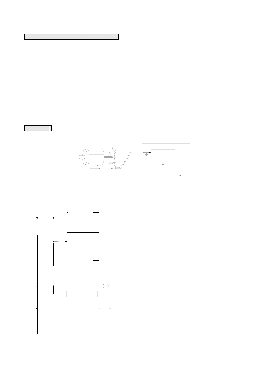
This example uses HSTA as a cyclic timer, cooperating with HSC0, to read the time interval for accumulation of 10
pulses and sending an interrupt out each time as 10 pulses are accumulated and, reciprocally, find out the required RPM
(the number of pulses is fixed when the time varies).
Mechanism
HSTA
HSC0
FUN92
U
X0
INT
PLC
Motor
(Y0 motor driving)
(X1 starting switch)
Light chopper
(1 pulse/revolution)
HSC and HST configuration
c
As HSTA is built in, no configuration is required. Simply make PV =0 to make it as a 32-bit cyclic timer.
d
To cooperate with the photo interrupter, set the HSC0 as an up counting counter having single input
(MD0, but use only U input).
※ All other settings (polarity of counting and control inputs) are preset (non-inverse) and should not be changed.
1 0 - 2 7
【
Main Program
】
1
JMP
EN
U/S
EN
R4
Sb :
D :
R6
Sa :
12D.(-)
R2
BR
CY
D=0
EN
M1
X1
M1924
EN
EN
HSCTR HSTA
R2
D :
66
08D.MOV
S :
R4152
Y0
CN:
HSTA
92
D :
PV
93D.HSCTW
S :
0
EN
EN
M1924
0
S :
93D.HSCTW
CN:
D :
S :
HSC0
PV
10
D :
CN:
CV
HSC0
93D.HSCTW
D=0
Sa : 6000000
EN
65
LBL
1
U/S
D :
Sb :
M1
R6
ERR
14D.( )
R100
•
Employ FUN93 to write current value 0 into the CV of HSC0 in
SoC chip (reset)
CN =0,
represents
HSC0
D =0,
represents
CV
• Write 10 into the preset register in SoC chip, which acts as
interrupt value for counting up;
FUN93 CN=0 indicates HSC0 and D=1 indicates PV
• Write 0 into the preset register, and HSTA is configured as a
32-bit high-speed cyclic timer
FUN93 CN=4 indicates HSTA and D=1 indicates PV
• Read the current timing value
• The initial value of HSTA CV register is stored to DR2
• Find interval for each HSC0 interrupt
•
RPM
60
T
N
speed
Rotating
×
∆
=
N=10,
S
10000
previousCV
currentCV
S
m
1
.
0
CV
T
)
(
-
∆
∆
=
×
=
Therefore
RPM
CV
6000000
speed
rotating
∆
=
• R100=RPM
• Clear the calculation flag of RPM
1 0 - 2 8
【Subroutine】
R TI
93D .H S C TW
69
E N
H S C 0
C N :
D :
C V
S :
0
M 1
08D .M O V
H S C 0I
08D .M O V
H S C TR
92
E N
E N
E N
65
LB L
R 4152
S :
D :
R 2
D :
S :
R 4
R 2
H S TA
• Each time when HSC0 accumulates 10 pulses, the
hardware will automatically run this interrupt subroutine
• Read the HSTA CV
• Reset the current value to 0
• M1=ON, RPM calculating flag
X0
HSC0I
∆
T =
8
9
10
1
10 1
9
10
1
10
10
10
10
10
10
=1200RPM
=10RPM
HSC0
CV value
PV value
10000
(1s)
V value of HSTA
1ms time basc)
15000
(1.5s)
200000
(20s)
800000
(80s)
DT = 0.5s
DT = 60s
N
RPM= x60
∆
T
N
RPM= x60
∆
T
RPM=
RPM=
CV value of HSTA
(0.1mS time base)
1 0 - 2 9
Example 3 HSTA serve as timely interrupt timer program
【Main Program】
M 0
5
PV
HSTA
CN:
D :
S :
93DP.HSCTW
EN
• Set up the period of timely interrupt time. S=5 represents
that it performs the interrupt service subroutine with the
label name of HSTAI every 0.5mS.
•
Employ FUN93 to write the preset value into HSTA PV in
SoC chip, which serve as time up for interrupt preset value.
CN =4, represents HSTA
D =1,
represents
PV
【Subroutine】
74.IMDI0
RTI
N :
69
EN
D :
Y0
1
17D.CMP
HSTAI
HSCTR
92
U/S
EN
EN
65
LBL
R4096
Sb :
Sa :
R0
a>b
a<b
Y0
a=b
HSC0
• Interrupt service subroutine with the label name of HSTA.
• Read the current value of hardware high speed counter HSC0
once every 0.5mS.
• To tell whether the current counting value is greater than or
equal to R0. if yes, then Y0 will be ON.
• Update output Y0 immediately, so as to reach the high speed
output reaction
(otherwise there will be introduced a delay in scan time)
1 0 - 3 0
10.6.4 Examples for Application of High-Speed Timer HST0~HST3
HSC and HST configuration(Using WinProladder)
Click the item “I/O Configuration” which in Project Windows :
Project name
System Configuration
I/O Configuration
Æ Select “Timer/Counter”
●
When “Timer/Counter” windows appear, then you can choose the “Hardware Timer” in Counter Type item, then HHSC
(Hardware High Speed Counter) can configure to be HHT.(Hardware High speed Timer)
●
User don’t have to configure the HSTA, because the HSTA is default. Only you want HHSC(Hardware High Speed
Counter) to be HHT.(Hardware High speed Timer) and you have to configure it.
HSC and HST configuration(Using FP-08)
• HSC0 is set as HST0
• HSC1 is preset as HSC
• HSC1 is set as MD0, an up counting counter with single
input. Other inputs will not be used.
•
All other settings (polarity of counting and control inputs) are default (Non-inverse) and should not be changed.
1 0 - 3 1
Example1 Application example for delay timer
This example configures HSC0 as a HST0 delay timer. At the same time, by connecting the high-speed counter
HSC1 with a rotary motor of an automatic wood drilling machine and sending out an interrupt at a fixed period. Each time
interrupt occur will read the counting value of the counter. Then, by comparing the change in speed between the number
of the motor’s rotation when no loading is applied (operating without drilling) and that when the drill head is pressing down
(drilling), the change of the motor’s RPM can be calculated. It is understood that resistance will be less and motor’s RPM
will be faster when the drill head is normal (sharp) than when the drill head is blunt. When the drill head is broken, it works
like operating without drilling that no resistance exists and RPM is the fastest. Usually the difference in rotating speed
among the three conditions is not significant and which cannot be sampled and detected by an ordinary timer having a
more than tens of ms of deviation. However, applied with an HST having a time base of 0.1mS that incorporating
interrupt, the drill head’s status (normal, blunt or broken) can be detected and, thus, warning can be given or operation
can be stopped in due time for drill head replacement.【The time is fixed and the number of pulses varies】
Mechanism
HST0
HSC1
FUN92
U
X4
INT
PLC
Motor
(Y0 motor driving)
(X1 starting switch)
Light chopper
(8 pulses/revolution)
【Main Program】
Y 8
D :
0
S :
E N
E N
E N
T 0
X 1
5 0 0
T 0
T U P
3
R 0
R 1 0 0
1 1 2 . B K C M P
R s :
L :
T s :
E R R
H S T 0
C V
. 0 1 S
C N :
D :
Y 0
E N
E N
M 1 9 2 4
9 3 D . H S C T W
H S T 0
5 0
9 3 D . H S C T W
P V
D :
C N :
S :
C V
H S C 1
0
9 3 D . H S C T W
C N :
D :
S :
• Employ FUN93 to reset current value register in SoC chip.
FUN93 CN=1 indicates HSC1 and D=0 indicates CV
• HST0 PV value is set as 50, i.e. one interrupt every 5mS
(50
×0.1mS)
• The initial value of HST0 CV register is 0
• Use FUN112 to compare the drill head’s RPM speed after
starting the motor for 5 seconds
R0: The number of HSC1 pulses obtained in every 5mS
1 0 - 3 2
【Subroutine】
R T I
6 9
D :
C N :
P V
H S T 0
1 1 D . ( + )
9 3 D . H S C T W
0 8 D . M O V
E N
U / S
E N
E N
5 0
S b :
R 4 0 9 8
S :
R 4 0 9 8
D :
B R
C Y
R 4 0 9 8
S a :
R 4 1 0 0
D :
S :
R 2
D = 0
H S T 0 I
1 2 D . ( - )
H S C T R
9 2
U / S
E N
E N
6 5
L B L
R 4 1 0 0
S b :
D :
S a :
R 2
R 0
B R
C Y
D = 0
H S C 1
• The hardware will execute this subroutine once every 5mS
• Read the current counting value of HSC1 and put it into
DR4100
• Find out the increment of HSC1 CV value in this 5mS
interval and store the value into DR0
• Calculate the new HSC0 PV
【Description】
Supposed that the drill head’s normal RPM is 18000rpm and the photo interrupter will generate 8 pulses in one
revolution, then the frequency of the pin U of HSC1 is 18000/60
×8=2400Hz, i.e. 12 pulses will be generated for
every 5mS. Therefore, HST0 can be used to send an interrupt and read the HSC1 CV value every 5mS to get
the RPM value.
1 0 - 3 3
X4
HST0I
∆T
DT = 5mS
(50 x 0.1mS)
DT = 5mS
(50 x 0.1mS)
DT = 5mS
(50 x 0.1mS)
∆
CV=12
(24 - 12)
∆
CV=12
(36 - 24)
∆
CV=12
(47 - 36)
11
12
13
23
24
25
35
36
37
46
47
48
50
100
150
200
50
100
150
200
HSC1
CV value
HSC0
CV value
HST0
PV value
(0.1mS time base)
HSC1
increased value
Upper Limit Lower Limit
R101 R100
←─────→
R0
(△CV)
───→ Y8
※ Setting different upper and lower
limits to category the RPM condition
R103 R102
←─────→
───→ Y9
R105 R104
←─────→
───→ Y10
Example2 Hardware high speed timer HST3 serve as 32-bit cyclic timer
M 300
M 300
HSCTR
EN
92
D :
HST3
CV
S :
CN :
0
HST3
93DP.HSCTW
EN
•
As M300 change from 0→1,
clear the current value register to 0
•
Employ FUN 93 to write current value 0 into the HST3 CV
(reset) in SoC chip
CN =3, represents HST3
D =0,
represents
CV
•
Employ FUN92 to read out the current timing value of HST3
in SoC chip and store it into the current value register
DR4108
(DR4108 value cyclically changes from 0, 1, 2, ……,
FFFFFFFF, 0, 1, 2, …… the unit is 0.1mS)
CN =3, represents HST3
1 0 - 3 4
Example3 Hardware high speed timer HST3 serve as periodic interrupt timer
【Main Program】
M1924
M300
M301
EN
145P
EN
HST3I
146P
93DP.HSCTW
EN
CN:
D :
S :
D :
HST3
PV
5
CV
93DP.HSCTW
EN
S :
CN:
EN
DIS
0
HST3
HST3I
• Turn on or M301 is ON, it prohibits the HST3 from sending
periodic interrupt
• As M300 change from 0→1, clear the current register to 0
• Employ FUN93 to write current value 0 into the HST3 CV (reset)
in SoC chip.
CN =3, represents HST3; D=0, represents CV
• Set up periodic interrupt interval; PV=5 represent every 0.5mS
perform once the interrupt service subroutine with label name of
HST3I.
• Employ FUN93 to write the preset value into the HST3 PV in SoC
chip, which serve as time up interrupt preset value.
CN=3 represents HST3; D=1 represents PV
• Enable the HST3 interrupt
【Subroutine】
R T I
S :
C N :
D :
6 9
E N
H S T 3
C V
0
9 3 D .H S C T W
N :
7 4 .IM D I0
D :
R s :
T s :
1 1 2 .B K C M P
D :
L :
H S T 3 I
9 2
H S C T R
E N
E N
6 5
L B L
E N
Y 8
8
R 1 0 0 0
8
Y 8
R 4 0 9 6
E R R
H S C 0
• Hardware high speed Interrupt service subroutine with the label
name of HST3I.
• Read the current value of hardware high speed counter HSC0
once every 0.5mS.
• To tell which zone of the electronic drum does the current
counting value fall, and set the corresponding output point to
be ON.
• Update output Y8~Y15 immediately
• Employ FUN93 to reset current value register into the HST3
CV in SoC chip (reset).
CN=3 represents HST3; D =0, represents CV
Wyszukiwarka
Podobne podstrony:
Figures for chapter 10
Intro to ABAP Chapter 10
Dictionary Chapter 10
Chapter 10 Relation between different kinds of stratigraphic units
Chapter 10 Falling part 2
English Skills with Readings 5e Chapter 10
durand word files Chapter 10 05753 10 ch10 p386 429 Caption
Figures for chapter 10
durand word files Chapter 10 05753 10 ch10 p386 429
Exploring Economics 4e Chapter 10
Ars Moriendi by vanilladoubleshot (chapters 1 10)
Essential College Experience with Readings Chapter 10
Chapter 10 Falling part 3
Chapter 10 Falling part 1
FENG YU JIU TIAN VOLUME 8 CHAPTER 10
DZIEWCZYNY Z AKADEMII GALLAGERA chapter 10
CHAPTER 10
więcej podobnych podstron