One Technology Way, P.O. Box 9106, Norwood. MA 02062-9106, U.S.A.
Tel: 617/329-4700
Fax: 617/326-8703
FUNCTIONAL BLOCK DIAGRAMS
REV. 0
Information furnished by Analog Devices is believed to be accurate and
reliable. However, no responsibility is assumed by Analog Devices for its
use, nor for any infringements of patents or other rights of third parties
which may result from its use. No license is granted by implication or
otherwise under any patent or patent rights of Analog Devices.
a
+3.3 V/+5 V Multiplying
12-Bit DACs
AD7943/AD7945/AD7948
FEATURES
12-Bit Multiplying DACs
Guaranteed Specifications with +3.3 V/+5 V Supply
0.5 LSBs INL and DNL
Low Power: 5
µ
W typ
Fast Interface
40 ns Strobe Pulse Width (AD7943)
40 ns Write Pulse Width (AD7945, AD7948)
Low Glitch: 60 nV-s with Amplifier Connected
Fast Settling: 600 ns to 0.01% with AD843
APPLICATIONS
Battery-Powered Instrumentation
Laptop Computers
Upgrades for All 754x Series DACs (5 V Designs)
GENERAL DESCRIPTION
The AD7943, AD7945 and AD7948 are fast 12-bit multiplying
DACs that operate from a single +5 V supply (Normal Mode)
and a single +3.3 V to +5 V supply (Biased Mode). The
AD7943 has a serial interface, the AD7945 has a 12-bit parallel
interface, and the AD7948 has an 8-bit byte interface. They will
replace the industry-standard AD7543, AD7545 and AD7548
in many applications, and they offer superior speed and power
consumption performance.
The AD7943 is available in 16-pin DIP, 16-pin SOP (Small
Outline Package) and 20-pin SSOP (Shrink Small Outline
Package).
The AD7945 is available in 20-pin DIP, 20-pin SOP and 20-pin
SSOP.
The AD7948 is available in 20-pin DIP, 20-pin SOP and 20-pin
SSOP.
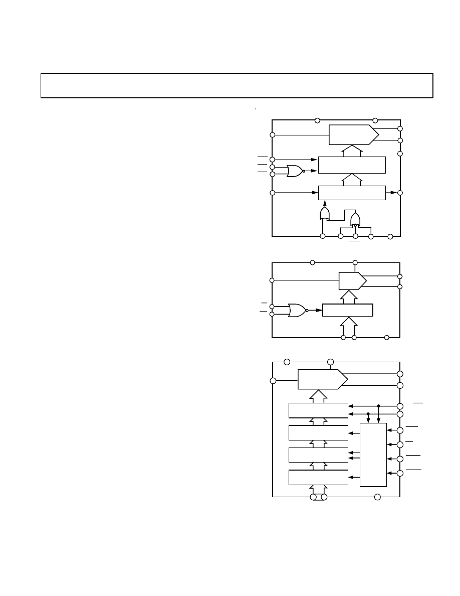
I
OUT1
I
OUT2
AGND
SRO
DGND
STB4
STB3
STB2
STB1
12-BIT DAC
R
FB
V
DD
CLR
LD1
LD2
V
REF
SRI
AD7943
DAC REGISTER
INPUT SHIFT REGISTER
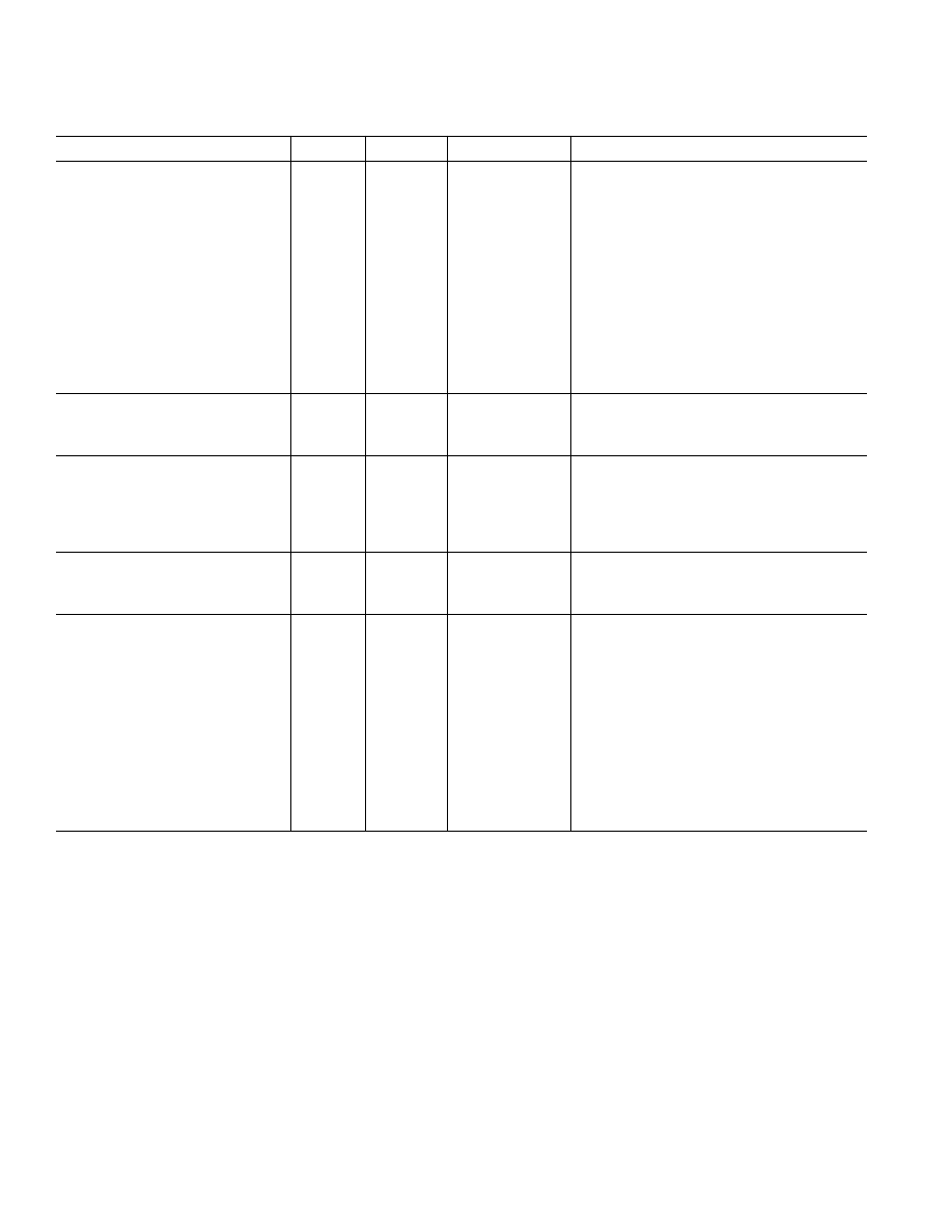
V
DD
CS
WR
DGND
R
FB
IOUT1
AGND
12-BIT
DAC
INPUT LATCH
DB11–DB0
12
12
AD7945
V
REF
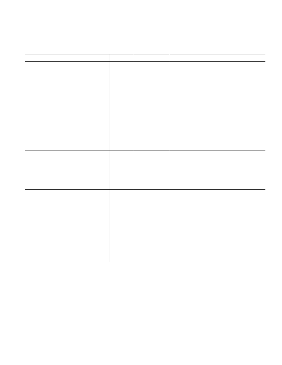
DATA OVERRIDE LOGIC
DATA STEERING LOGIC
INPUT REGISTERS
DAC REGISTER
8
12
12
12
12
DB7–DB0
DGND
CTRL
AGND
I
OUT1
R
FB
V
DD
V
REF
DF/DOR
LDAC
WR
CSLSB
CSMSB
AD7948
CONTROL
LOGIC
12-BIT DAC
REV. 0
–2–
AD7943/AD7945/AD7948–SPECIFICATIONS
1
Parameter
B Grades
2
T Grade
2, 3
Units
Test Conditions/Comments
ACCURACY
Resolution
12
12
Bits
1 LSB = V
REF
/2
12
= 2.44 mV when V
REF
= 10 V
Relative Accuracy
±
0.5
±
0.5
LSB max
Differential Nonlinearity
±
0.5
±
0.5
LSB max
All Grades Guaranteed Monotonic over
Temperature
Gain Error
T
MIN
to T
MAX
±
2
±
2
LSB max
Gain Temperature Coefficient
4
2
2
ppm FSR/
°
C typ
5
5
ppm FSR/
°
C max
Output Leakage Current
I
OUT1
@ +25
°
C
10
10
nA max
See Terminology Section
T
MIN
to T
MAX
100
100
nA max
Typically 20 nA over Temperature
REFERENCE INPUT
Input Resistance
6
6
k
Ω
min
Typical Input Resistance = 9 k
Ω
12
12
k
Ω
max
DIGITAL INPUTS
V
INH
, Input High Voltage
2.4
2.4
V min
V
INL
, Input Low Voltage
0.8
0.8
V max
I
INH
, Input Current
±
1
±
1
µ
A max
C
IN
, Input Capacitance
4
10
10
pF max
DIGITAL OUTPUT (AD7943 SRO)
For 1 CMOS Load
Output Low Voltage (V
OL
)
0.2
0.2
V max
Output High Voltage (V
OH
)
V
DD
– 0.2
V
DD
– 0.2
V min
POWER REQUIREMENTS
V
DD
Range
4.5/5.5
4.5/5.5
V min/V max
Power Supply Sensitivity
4
∆
Gain/
∆
V
DD
–75
–75
dB typ
I
DD
(AD7943)
5
5
µ
A max
V
INH
= V
DD
– 0.1 V min, V
INL
= 0.1 V max.
SRO Open Circuit. No STB Signal. Typically
1
µ
A. Typically 100
µ
A with a 1 MHz STB
Frequency. At Input Levels of 0.8 V and 2.4 V,
I
DD
Is Typically 2.5 mA.
I
DD
(AD7945, AD7948)
5
5
µ
A max
V
INH
= V
DD
– 0.1 V min, V
INL
= 0.1 V max.
Typically 1
µ
A. At Input Levels of 0.8 V and
2.4 V, I
DD
Is Typically 2.5 mA.
NOTES
1
The AD7943, AD7945 and AD7948 are specified in the normal current mode configuration and in the biased current mode for single-supply applications.
Figures 15 and 16 are examples of normal mode operation.
2
Temperature ranges as follows: B Grades: –40
°
C to +85
°
C; T Grade: –55
°
C to +125
°
C.
3
The T Grade applies to the AD7945 only.
4
Guaranteed by design.
Specifications subject to change without notice.
NORMAL MODE
(AD7943: V
DD
= +4.5 V to +5.5 V; V
IOUT1
= V
IOUT2
= AGND = 0 V; V
REF
= +10 V; T
A
= T
MIN
to T
MAX
, unless otherwise noted.
AD7945, AD7948: V
DD
= +4.5 V to +5.5 V; V
IOUT1
= AGND = 0 V; V
REF
= +10 V; T
A
= T
MIN
to T
MAX
, unless otherwise noted.)
AD7943/AD7945/AD7948
REV. 0
–3–
Parameter
A Grades
2
Units
Test Conditions/Comments
ACCURACY
Resolution
12
Bits
1 LSB = (V
IOUT1
– V
REF)
/2
12
= 300
µ
V When
V
IOUT1
= 1.23 V and V
REF
= 0 V
Relative Accuracy
±
1
LSB max
Differential Nonlinearity
±
0.9
LSB max
All Grades Guaranteed Monotonic
over Temperature
Gain Error @ +25
°
C
±
3
LSB max
T
MIN
to T
MAX
±
4
LSB max
Gain Temperature Coefficient
3
2
ppm FSR/
°
C typ
5
ppm FSR/
°
C max
Output Leakage Current
See Terminology Section
I
OUT1
@ +25
°
C
10
nA max
T
MIN
to T
MAX
100
nA max
Typically 20 nA over Temperature
Input Resistance
This Varies with DAC Input Code
@ I
OUT2
Pin (AD7943)
6
k
Ω
min
@ AGND Pin (AD7945, AD7948)
6
k
Ω
min
DIGITAL INPUTS
V
INH
, Input High Voltage @ V
DD
= +5 V
2.4
V min
V
INH
, Input High Voltage @ V
DD
= +3.3 V
2.1
V min
V
INL
, Input Low Voltage @ V
DD
= +5 V
0.8
V max
V
INL
, Input Low Voltage @ V
DD
= +3.3 V
0.6
V max
I
INH
, Input Current
±
1
µ
A max
C
IN
, Input Capacitance
3
10
pF max
DIGITAL OUTPUT (SRO)
For 1 CMOS Load
Output Low Voltage (V
OL
)
0.2
V max
Output High Voltage (V
OH
)
V
DD
– 0.2
V min
POWER REQUIREMENTS
V
DD
Range
3.0/5.5
V min/V max
Power Supply Sensitivity
3
∆
Gain/
∆
V
DD
–75
dB typ
I
DD
(AD7943)
5
µ
A max
V
INH
= V
DD
– 0.1 V min, V
INL
= 0.1 V max.
SRO Open Circuit; No STB Signal; Typically
1
µ
A. Typically 100
µ
A with 1 MHz STB
Frequency.
I
DD
(AD7945, AD7948)
5
µ
A max
V
INH
= V
DD
– 0.1 V min, V
INL
= 0.1 V max.
Typically 1
µ
A.
NOTES
1
These specifications apply with the devices biased up at 1.23 V for single supply applications. The model numbering reflects this by means of a “–B” suffix
(for example: AD7943AN-B). Figure 17 is an example of Biased Mode Operation.
2
Temperature ranges as follows: A Versions: –40
°
C to +85
°
C.
3
Guaranteed by design.
Specifications subject to change without notice.
BIASED MODE
SPECIFICATIONS
1
(AD7943: V
DD
= +3 V to +5.5 V; V
IOUT1
= V
IOUT2
= AGND = 1.23 V; V
REF
= +0 V to 2.45 V; T
A
= T
MIN
to T
MAX
, unless other-
wise noted. AD7945, AD7948: V
DD
= +3 V to +5.5 V; V
IOUT1
= AGND = 1.23 V; V
REF
= +0 V to 2.45 V; T
A
= T
MIN
to T
MAX
, unless otherwise noted.)
AD7943/AD7945/AD7948
REV. 0
–4–
AC PERFORMANCE CHARACTERISTICS
Normal Mode
Parameter
B Grades
T Grade
Units
Test Conditions/Comments
DYNAMIC PERFORMANCE
Output Voltage Settling Time
600
700
ns typ
To 0.01% of Full-Scale Range. V
REF
=
+10 V; DAC Latch Alternately Loaded with
All 0s and All 1s
Digital to Analog Glitch Impulse
60
60
nV-s typ
Measured with V
REF
= 0 V. DAC Latch
Alternately Loaded with All 0s and All 1s
Multiplying Feedthrough Error
–75
–75
dB max
DAC Latch Loaded with All 0s
Output Capacitance
60
60
pF max
All 1s Loaded to DAC
30
30
pF max
All 0s Loaded to DAC
Digital Feedthrough (AD7943)
5
5
nV-s typ
Feedthrough to the DAC Output with LD1,
LD2
High and Alternate Loading of All 0s
and All 1s into the Input Shift Register
Digital Feedthrough (AD7945, AD7948) 5
5
nV-s typ
Feedthrough to the DAC Output with CS
High and Alternate Loading of All 0s and
All 1s to the DAC Bus
Total Harmonic Distortion
–83
–83
dB typ
Output Noise Spectral Density
@ 1 kHz
35
35
nV/
√
Hz
typ
All 1s Loaded to DAC. V
REF
= 0 V. Output
Op Amp Is OP07
(AD7943: V
DD
= +4.5 V to +5.5 V; V
IOUT1
= V
IOUT2
= AGND = 0 V. AD7945, AD7948: V
DD
= +4.5 V to +5.5 V; V
IOUT1
= AGND
= 0 V. V
REF
= 6 V rms, 1 kHz sine wave; T
A
= T
MIN
to T
MAX
; DAC output op amp is AD843; unless otherwise noted.) These characteristics are
included for Design Guidance and are not subject to test.
AC PERFORMANCE CHARACTERISTICS
Biased Mode
(AD7943: V
DD
= +3 V to +5.5 V; V
IOUT1
= V
IOUT2
= AGND = 1.23 V. AD7945, AD7948: V
DD
= +3 V to +5.5 V; V
IOUT1
= AGND =
1.23 V. V
REF
= 1 kHz, 2.45 V p-p, sine wave biased at 1.23 V; DAC output op amp is AD820; T
A
= T
MIN
to T
MAX
; unless otherwise noted.) These
characteristics are included for Design Guidance and are not subject to test.
Parameter
A Grades
Units
Test Conditions/Comments
DYNAMIC PERFORMANCE
Output Voltage Settling Time
5
µ
s typ
To 0.01% of Full-Scale Range. V
REF
= 0 V
DAC Latch Alternately Loaded with All 0s and All 1s
Digital to Analog Glitch Impulse
60
nV-s typ
V
REF
= 1.23 V. DAC Register Alternately Loaded
with All 0s and All 1s
Multiplying Feedthrough Error
–75
dB max
DAC Latch Loaded with All 0s
Output Capacitance
60
pF max
All 1s Loaded to DAC
30
pF max
All 0s Loaded to DAC
Digital Feedthrough
5
nV-s typ
Feedthrough to the DAC Output with LD1, LD2
High and Alternate Loading of All 0s and All 1s
into the Input Shift Register
Digital Feedthrough (AD7945, AD7948)
5
nV-s typ
Feedthrough to the DAC Output with CS High
and Alternate Loading of All 0s and All 1s to the
DAC Bus
Total Harmonic Distortion
–83
dB typ
Output Noise Spectral Density
@ 1 kHz
25
nV/
√
Hz
typ
All 1s Loaded to DAC. V
REF
= 1.23 V
AD7943/AD7945/AD7948
REV. 0
–5–
(T
A
= T
MIN
to T
MAX
, unless otherwise noted)
Limit @
Limit @
Parameter
V
DD
= +3 V to +3.6 V
V
DD
= +4.5 V to +5.5 V
Units
Description
t
STB
2
60
40
ns min
STB Pulse Width
t
DS
15
10
ns min
Data Setup Time
t
DH
35
25
ns min
Data Hold Time
t
SRI
55
35
ns min
SRI Data Pulse Width
t
LD
55
35
ns min
Load Pulse Width
t
CLR
55
35
ns min
CLR Pulse Width
t
ASB
0
0
ns min
Min Time Between Strobing Input Shift
Register and Loading DAC Register
t
SV
3
60
35
ns max
STB Clocking Edge to SRO Data Valid Delay
NOTES
1
All input signals are specified with tr = tf = 5 ns (10% to 90% of 5 V) and timed from a voltage level of 1.6 V. tr and tf should not exceed 1
µ
s on any digital input.
2
STB mark/space ratio range is 60/40 to 40/60.
3
t
SV
is measured with the load circuit of Figure 2 and defined as the time required for the output to cross 0.8 V or 2.4 V.
SRI
STB1,
STB2,
STB4
STB3
DB11(N)
(MSB)
DB10(N)
LD1.LD2
CLR
t
STB
t
DS
SRO
DB11(N–1)
(MSB)
DB10(N–1)
DB0(N–1)
t
DH
t
SRI
t
LD
,
t
CLR
t
ASB
t
SV
DB0(N)
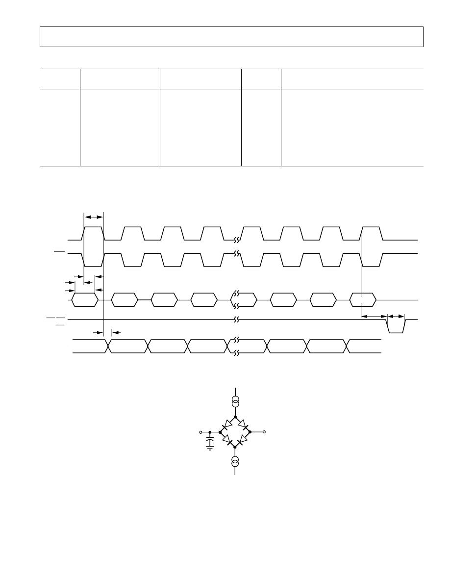
Figure 1. AD7943 Timing Diagram
TO OUTPUT
PIN
+2.1V
I
OL
C
L
50pF
1.6mA
200
µ
A
I
OH
Figure 2. Load Circuit for Digital Output Timing Specifications
AD7943 TIMING SPECIFICATIONS
1
AD7943/AD7945/AD7948
REV. 0
–6–
AD7945 TIMING SPECIFICATIONS
1
(T
A
= T
MIN
to T
MAX
, unless otherwise noted)
Limit @
Limit @
Parameter
V
DD
= +3 V to +3.6 V
V
DD
= +4.5 V to +5.5 V
Units
Description
t
DS
35
20
ns min
Data Setup Time
t
DH
10
10
ns min
Data Hold Time
t
CS
60
40
ns min
Chip Select Setup Time
t
CH
0
0
ns min
Chip Select Hold Time
t
WR
60
40
ns min
Write Pulse Width
NOTE
1
All input signals are specified with tr = tf = 5 ns (10% to 90% of 5 V) and timed from a voltage level of 1.6 V.
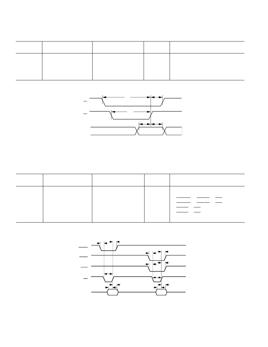
CS
WR
DB11–DB0
t
DH
t
DS
t
WR
t
CH
t
CS
DATA VALID
Figure 3. AD7945 Timing Diagram
AD7948 TIMING SPECIFICATIONS
1
(T
A
= T
MIN
to T
MAX
, unless otherwise noted)
Limit @
Limit @
Parameter
V
DD
= +3 V to +3.6 V
V
DD
= +4.5 V to +5.5 V
Units
Description
t
DS
45
30
ns min
Data Setup Time
t
DH
10
10
ns min
Data Hold Time
t
CWS
0
0
ns min
CSMSB
or CSLSB to WR Setup Time
t
CWH
0
0
ns min
CSMSB
or CSLSB to WR Hold Time
t
LWS
0
0
ns min
LDAC
to WR Setup Time
t
LWH
0
0
ns min
LDAC
to WR Hold Time
t
WR
60
40
ns min
Write Pulse Width
NOTE
1
All input signals are specified with tr = tf = 5 ns (10% to 90% of 5 V) and timed from a voltage level of 1.6 V.
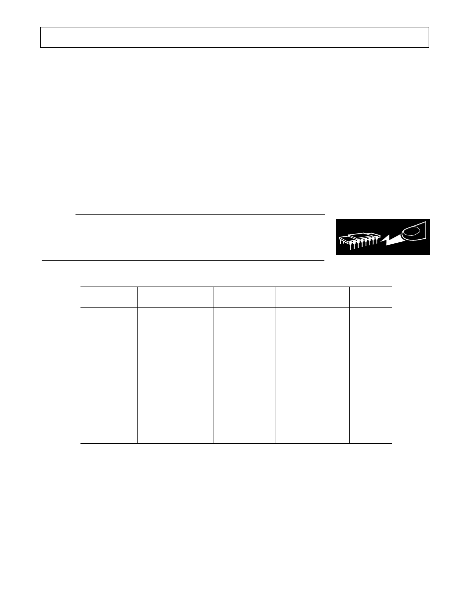
DB7– DB0
CSMSB
CSLSB
LDAC
WR
DATA
VALID
DATA
VALID
t
CWS
t
CWH
t
WR
t
DS
t
DS
t
DS
t
DH
t
DH
t
WR
t
LWS
t
LWH
t
CWS
t
CWH
Figure 4. AD7948 Timing Diagram
AD7943/AD7945/AD7948
REV. 0
–7–
ORDERING GUIDE
Temperature
Linearity
Nominal
Package
Model
Range
Error (LSBs)
Supply Voltage
Option
1
AD7943BN
–40
°
C to +85
°
C
±
0.5
+5 V
N-16
AD7943BR
–40
°
C to +85
°
C
±
0.5
+5 V
R-16
AD7943BRS
–40
°
C to +85
°
C
±
0.5
+5 V
RS-20
AD7943AN-B
–40
°
C to +85
°
C
±
1
+3.3 V to +5 V
N-16
AD7943ARS-B
–40
°
C to +85
°
C
±
1
+3.3 V to +5 V
RS-20
AD7945BN
–40
°
C to +85
°
C
±
0.5
+5 V
N-20
AD7945BR
–40
°
C to +85
°
C
±
0.5
+5 V
R-20
AD7945BRS
–40
°
C to +85
°
C
±
0.5
+5 V
RS-20
AD7945AN-B
–40
°
C to +85
°
C
±
1
+3.3 V to +5 V
N-20
AD7945ARS-B
–40
°
C to +85
°
C
±
1
+3.3 V to +5 V
RS-20
AD7945TQ
–55
°
C to +125
°
C
±
1
+5 V
Q-20
AD7948BN
–40
°
C to +85
°
C
±
0.5
+5 V
N-20
AD7948BR
–40
°
C to +85
°
C
±
0.5
+5 V
R-20
AD7948BRS
–40
°
C to +85
°
C
±
0.5
+5 V
RS-20
AD7948AN-B
–40
°
C to +85
°
C
±
1
+3.3 V to +5 V
N-20
AD7948ARS-B
–40
°
C to +85
°
C
±
1
+3.3 V to +5 V
RS-20
NOTE
1
N = Plastic DIP; R = SOP (Small Outline Package); RS = SSOP (Shrink Small Outline Package); Q = Cerdip.
ABSOLUTE MAXIMUM RATINGS
1
(T
A
= +25
°
C unless otherwise noted)
V
DD
to DGND . . . . . . . . . . . . . . . . . . . . . . . . . .–0.3 V to +6 V
I
OUT1
to DGND . . . . . . . . . . . . . . . . . . . –0.3 V to V
DD
+ 0.3 V
I
OUT2
to DGND . . . . . . . . . . . . . . . . . . . –0.3 V to V
DD
+ 0.3 V
AGND to DGND . . . . . . . . . . . . . . . . . –0.3 V to V
DD
+ 0.3 V
Digital Input Voltage to DGND . . . . . . –0.3 V to V
DD
+ 0.3 V
V
RFB
, V
REF
to DGND . . . . . . . . . . . . . . . . . . . . . . . . . .
±
15 V
Input Current to Any Pin Except Supplies
2
. . . . . . . .
±
10 mA
Operating Temperature Range
Industrial (A, B Versions) . . . . . . . . . . . . . . –40
°
C to +85
°
C
Extended (T Version) . . . . . . . . . . . . . . . . –55
°
C to +125
°
C
Storage Temperature Range . . . . . . . . . . . . –65
°
C to +150
°
C
Junction Temperature . . . . . . . . . . . . . . . . . . . . . . . . . +150
°
C
DIP Package, Power Dissipation . . . . . . . . . . . . . . . . 670 mW
θ
JA
Thermal Impedance . . . . . . . . . . . . . . . . . . . . . 116
°
C/W
Lead Temperature, Soldering, (10 sec) . . . . . . . . . . +260
°
C
SOP Package, Power Dissipation . . . . . . . . . . . . . . . . . 450 mW
θ
JA
Thermal Impedance . . . . . . . . . . . . . . . . . . . . . . 75
°
C/W
Lead Temperature, Soldering
Vapor Phase (60 sec) . . . . . . . . . . . . . . . . . . . . . . +215
°
C
Infrared (15 sec) . . . . . . . . . . . . . . . . . . . . . . . . . . +220
°
C
SSOP Package, Power Dissipation . . . . . . . . . . . . . . . . 875 mW
θ
JA
Thermal Impedance . . . . . . . . . . . . . . . . . . . . . 132
°
C/W
Lead Temperature, Soldering
Vapor Phase (60 sec) . . . . . . . . . . . . . . . . . . . . . . +215
°
C
Infrared (15 sec) . . . . . . . . . . . . . . . . . . . . . . . . . . +220
°
C
NOTES
1
Stresses above those listed under “Absolute Maximum Ratings” may cause
permanent damage to the device. This is a stress rating only and functional
operation of the device at these or any other conditions above those listed in the
operational sections of this specification is not implied. Exposure to absolute
maximum rating conditions for extended periods may affect device reliability.
2
Transient currents of up to 100 mA will not cause SCR latch-up.
WARNING!
ESD SENSITIVE DEVICE
CAUTION
ESD (electrostatic discharge) sensitive device. Electrostatic charges as high as 4000 V readily
accumulate on the human body and test equipment and can discharge without detection.
Although the devices feature proprietary ESD protection circuitry, permanent damage may occur
on devices subjected to high energy electrostatic discharges. Therefore, proper ESD precautions
are recommended to avoid performance degradation or loss of functionality.
AD7943/AD7945/AD7948
REV. 0
–8–
TERMINOLOGY
Relative Accuracy
Relative Accuracy or endpoint linearity is a measure of the
maximum deviation from a straight line passing through the
endpoints of the DAC transfer function. It is measured after
adjusting for zero error and full-scale error and is normally
expressed in Least Significant Bits or as a percentage of full-
scale reading.
Differential Nonlinearity
Differential nonlinearity is the difference between the measured
change and the ideal 1 LSB change between any two adjacent
codes. A specified differential nonlinearity of 1 LSB maximum
ensures monotonicity.
Gain Error
Gain Error is a measure of the output error between an ideal
DAC and the actual device output. It is measured with all 1s
in the DAC after offset error has been adjusted out and is ex-
pressed in Least Significant Bits. Gain error is adjustable to
zero with an external potentiometer.
Output Leakage Current
Output leakage current is current which flows in the DAC lad-
der switches when these are turned off. For the I
OUT1
terminal,
it can be measured by loading all 0s to the DAC and measuring
the I
OUT1
current. Minimum current will flow in the I
OUT2
line
when the DAC is loaded with all 1s.
Output Capacitance
This is the capacitance from the I
OUT1
pin to AGND.
Output Voltage Settling Time
This is the amount of time it takes for the output to settle to a
specified level for a full-scale input change. For these devices, it
is specified both with the AD843 as the output op amp in the
normal current mode and with the AD820 in the biased current
mode.
Digital to Analog Glitch Impulse
This is the amount of charge injected into the analog output
when the inputs change state. It is specified as the area of the
glitch in nV-s. It is measured with the reference input connected
to AGND and the digital inputs toggled between all 1s and all
0s. As with Settling Time, it is specified with both the AD817
and the AD820.
AC Feedthrough Error
This is the error due to capacitive feedthrough from the DAC
reference input to the DAC I
OUT1
terminal, when all 0s are
loaded in the DAC.
Digital Feedthrough
When the device is not selected, high frequency logic activity on
the device digital inputs is capacitively coupled through the de-
vice to show up as noise on the I
OUT1
pin and subsequently on
the op amp output. This noise is digital feedthrough.
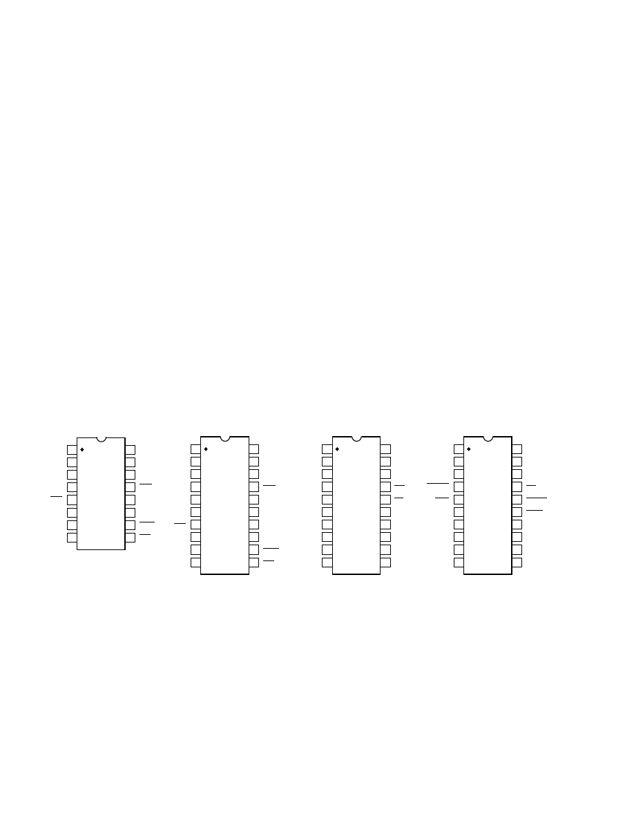
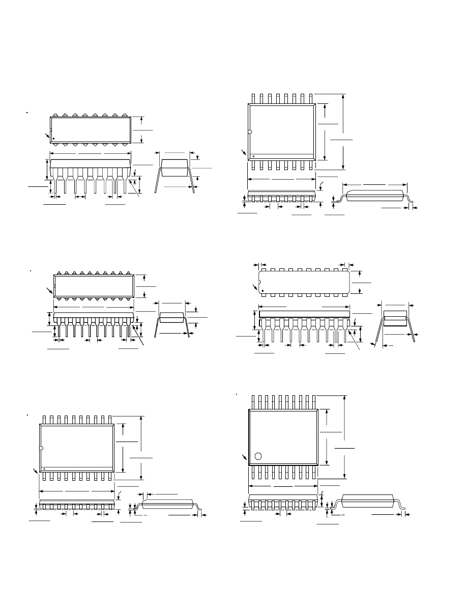
PIN CONFIGURATIONS
DIP/SOP
SSOP
DIP/SOP/SSOP
DIP/SOP/SSOP
I
OUT1
I
OUT2
R
FB
V
REF
LD1
SRO
SRI
DGND
STB4
STB3
AGND
STB1
V
DD
CLR
STB2
LD2
1
2
16
15
5
6
7
12
11
10
3
4
14
13
8
9
TOP VIEW
(Not to Scale)
AD7943
NC = NO CONNECT
I
OUT1
I
OUT2
R
FB
V
REF
NC
NC
LD1
NC
NC
DGND
AGND
STB1
V
DD
CLR
SRO STB4
SRI
STB3
STB2
LD2
1
2
20
19
5
6
7
16
15
14
3
4
18
17
8
13
9
12
10
11
TOP VIEW
(Not to Scale)
AD7943
I
OUT1
AGND
R
FB
V
REF
DB10
DB9
DB8
CS
DB0
DB1
DGND
DB11
V
DD
WR
DB7 DB2
DB6 DB3
DB5 DB4
1
2
20
19
5
6
7
16
15
14
3
4
18
17
8
13
9
12
10
11
TOP VIEW
(Not to Scale)
AD7945
I
OUT1
AGND
R
FB
V
REF
DF/
DOR
CTRL
DB7 (MSB)
CSLSB
LDAC
DB0 (LSB)
DGND
CSMSB
V
DD
WR
DB6 DB1
DB5
DB2
DB4 DB3
1
2
20
19
5
6
7
16
15
14
3
4
18
17
8
13
9
12
10
11
TOP VIEW
(Not to Scale)
AD7948
AD7943/AD7945/AD7948
REV. 0
–9–
AD7943 PIN DESCRIPTION
Pin Mnemonic
Description
I
OUT1
DAC current output terminal 1.
I
OUT2
DAC current output terminal 2. This should be connected to the AGND pin.
AGND
This pin connects to the back gates of the current steering switches. In normal operation, it should be connected
to the signal ground of the system. In biased single-supply operation it may be biased to some voltage between
0 V and the 1.23 V. See Figure 11 for more details.
STB 1
This is the Strobe 1 input. Data is clocked into the input shift register on the rising edge of this signal. STB 3
must be high. STB 2, STB 4 must be low.
LD1
, LD2
Active low inputs. When both of these are low, the DAC register is updated and the output will change to
reflect this.
SRI
Serial Data Input. Data on this line will be clocked into the input shift register on one of the Strobe inputs,
when they are enabled.
STB 2
This is the Strobe 2 input. Data is clocked into the input shift register on the rising edge of this signal.
STB 3
must be high. STB 1, STB 4 must be low.
STB 3
This is the Strobe 3 input. Data is clocked into the input shift register on the falling edge of this signal. STB 1,
STB 2, STB 4, must be low.
STB 4
This is the Strobe 4 input. Data is clocked into the input shift register on the rising edge of this signal. STB 3
must be high. STB 1, STB 2 must be low.
DGND
Digital Ground.
CLR
Asynchronous CLR input. When this input is taken low, all 0s are loaded to the DAC latch.
V
DD
Power supply input. This is nominally +5 V for Normal Mode Operation and +3.3 V to +5 V for Biased
Mode Operation.
V
REF
DAC reference input.
R
FB
DAC feedback resistor pin.
AD7945 PIN DESCRIPTION
Pin Mnemonic
Description
I
OUT1
DAC current output terminal 1.
AGND
This pin connects to the back gates of the current steering switches. The DAC I
OUT2
terminal is also connected
internally to this point.
DGND
Digital Ground.
DB11–DB0
Digital Data Inputs.
CS
Active Low, Chip Select Input.
WR
Active Low, Write Input.
V
DD
Power supply input. This is nominally +5 V for Normal Mode Operation and +3.3 V to +5 V for Biased Mode
Operation.
V
REF
DAC reference input.
R
FB
DAC feedback resistor pin.
AD7943/AD7945/AD7948
REV. 0
–10–
AD7948 PIN DESCRIPTION
Pin Mnemonic
Description
I
OUT1
DAC current output terminal 1. Normally terminated at the virtual ground of output amplifier.
AGND
Analog Ground Pin. This pin connects to the back gates of the current steering switches. The DAC I
OUT2
terminal is also connected internally to this point.
DGND
Digital Ground Pin.
CSMSB
Chip Select Most Significant Byte. Active Low Input. Used in combination with WR to load
external data into the input register or in combination with LDAC and WR to load external data into both input
and DAC registers.
DF/DOR
Data Format/Data Override. When this input is low, data in the DAC register is forced to one of two override
codes selected by CTRL. When the override signal is removed, the DAC output returns to reflect the value in
the DAC register. With DF/DOR high, CTRL selects either a left or right justified input data format. For normal
operation, DF/DOR is held high. See Table I.
CTRL
Control Input. See DF/DOR description.
DB7–DB0
Digital Data Inputs.
LDAC
Load DAC input, active low. This signal, in combination with others, is used to load the DAC register from
either the input register or the external data bus.
CSLSB
Chip Select Least Significant (LS) Byte. Active Low Input. Used in combination with WR to load external data
into the input register or in combination with WR and LDAC to load external data into both input and DAC
registers.
WR
Write input, active low. This active low signal, in combination with others is used in loading external data into
the AD7948 input register and in transferring data from the input register to the DAC register.
V
DD
Power supply input. This is nominally +5 V for Normal Mode Operation and +3.3 V to +5 V for Biased Mode
Operation.
V
REF
DAC reference input.
R
FB
DAC feedback resistor pin.
Table II. Truth Table for AD7948 Write Operation
WR
CSMSB
CSLSB
LDAC
Function
0
1
0
1
Load LS Byte to Input Register
0
1
0
0
Load LS Byte to Input Register and DAC Register
0
0
1
1
Load MS Byte to Input Register
0
0
1
0
Load MS Byte to Input Register and DAC Register
0
1
1
0
Load Input Register to DAC Register
1
X
X
X
No Data Transfer
Table I. Truth Table for DF/DOR CTRL
DF/DOR
CTRL
Function
0
0
DAC Register Contents Overridden by All 0s
0
1
DAC Register Contents Overridden by All 1s
1
0
Left-Justified Input Data Selected
1
1
Right-Justified Input Data Selected
AD7943/AD7945/AD7948
REV. 0
–11–
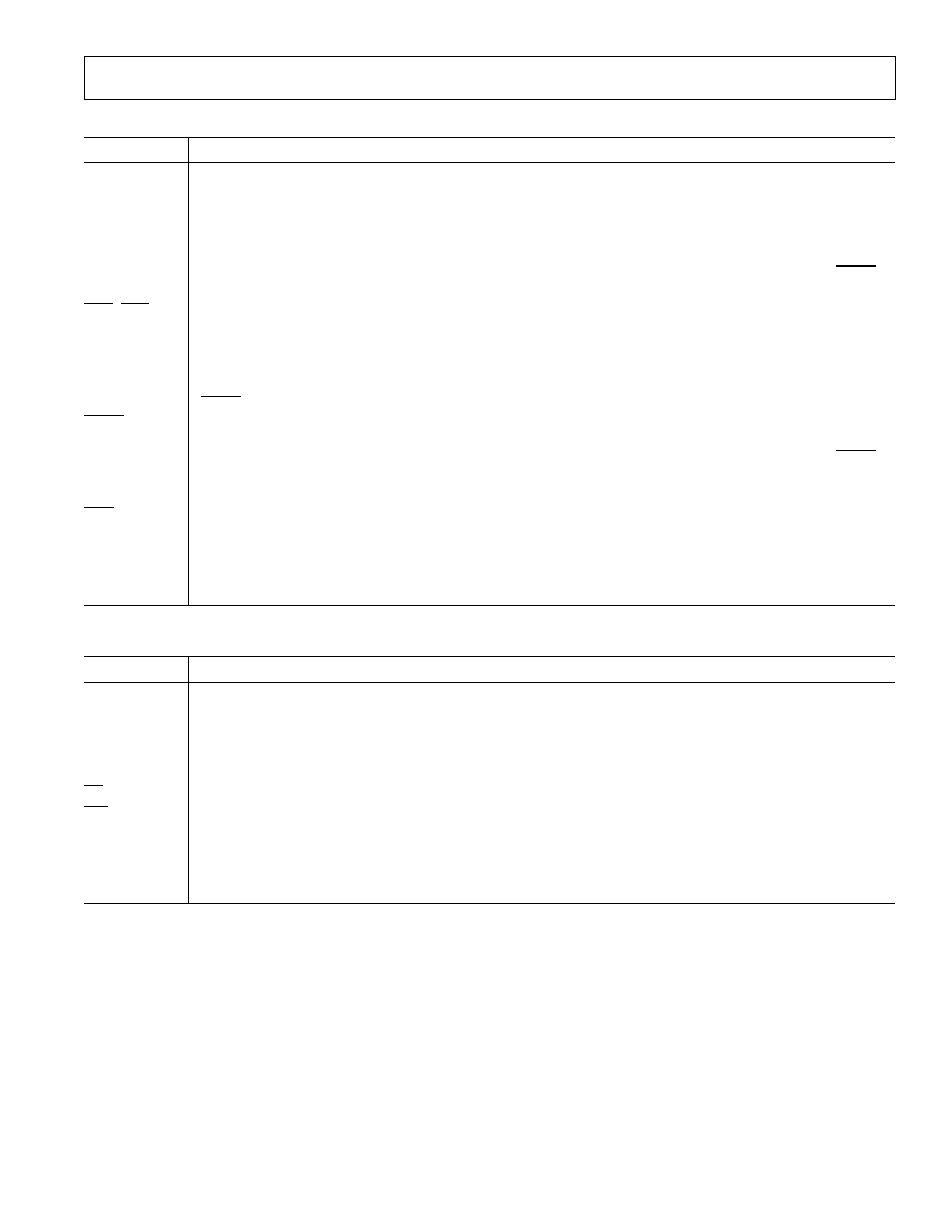
Typical Performance Curves
Figure 7. All Codes Linearity In Normal Mode (V
DD
= +5 V)
0.50
–0.50
0
4095
0.25
–0.25
1024
0.00
2048
3072
INPUT CODE
LINEARITY ERROR – LSBs
V
DD
= +5V
V
REF
= +10V
OP AMP = AD843
T
A
= +25
°
C
Figure 5. Differential Nonlinearity Error vs.
V
REF
(Normal Mode)
Figure 6. Integral Nonlinearity Error vs.
V
REF
(Normal Mode)
0.5
0
10
0.3
0.1
4
0.2
2
0.4
8
6
DNL – LSBs
V
REF
– Volts
V
DD
= +5V
T
A
= +25°C
OP AMP = AD843
1.0
0
10
0.3
0.1
4
0.2
2
0.6
0.4
0.5
0.7
0.8
0.9
8
6
INL – LSBs
V
REF
– Volts
V
DD
= +5V
T
A
= +25°C
OP AMP = AD843
INL, DNL – LSBs
V
REF
– V
BIAS
– Volts
6
0
1.4
3
1
0.4
2
0.2
5
4
1.2
1.0
0.8
0.6
V
DD
= +3.3V
T
A
= +25°C
OP AMP = AD820
Figure 8. Linearity Error vs. V
REF
(Biased Mode)
AD7943/AD7945/AD7948
REV. 0
–12–
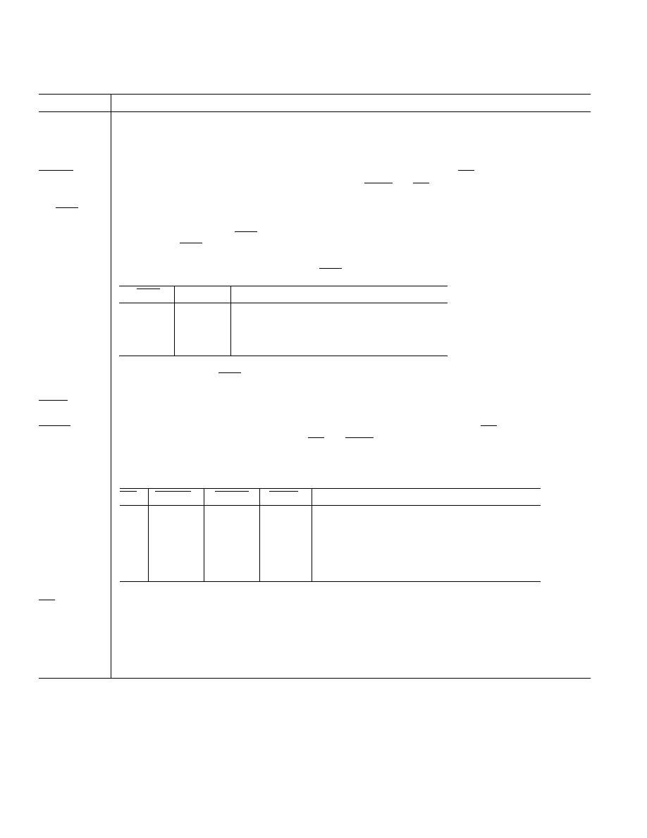
0
–100
10M
–70
–90
10k
–80
1k
–40
–60
–50
–30
–20
–10
1M
100k
V
DD
= +5V
T
A
= +25
°
C
V
IN
= 20V p-p
OP AMP = AD711
DAC LOADED WITH ALL 0s
DAC LOADED WITH ALL 1s
FREQUENCY – Hz
Figure 11. Digital-to-Analog Glitch Impulse
–50
–100
100k
–85
–95
1k
–90
100
–70
–80
–75
–65
–60
–55
10k
FREQUENCY – Hz
THD – dBs
V
DD
= +5V
T
A
= +25
°
C
V
IN
= 6V rms
OP AMP = AD711
Figure 10. Total Harmonic Distortion vs. Frequency
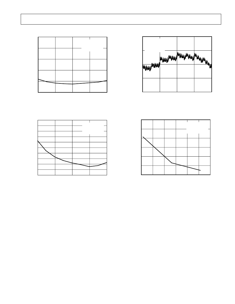
Figure 12. Multiplying Frequency Response vs.
Digital Code
Figure 9. All Codes Linearity in Biased Mode
(V
DD
= +3.3 V)
1.00
–1.00
0
4095
0.50
–0.50
1024
0.00
2048
3072
INPUT CODE
LINEARITY ERROR – LSBs
V
DD
= +3.3V
V
REF
= 0V
V
BIAS
= 1.23V
OP AMP = AD820
T
A
= +25
°
C
DIGITAL INPUTS
AD711 OUTPUT
5V/DIVISION 200ns/DIVISION
50mV/DIVISION 200ns/DIVISION
V
DD
= +5V
T
A
= +25°C
V
REF
= 0V
OP AMP = AD711
AD7943/AD7945/AD7948
REV. 0
–13–
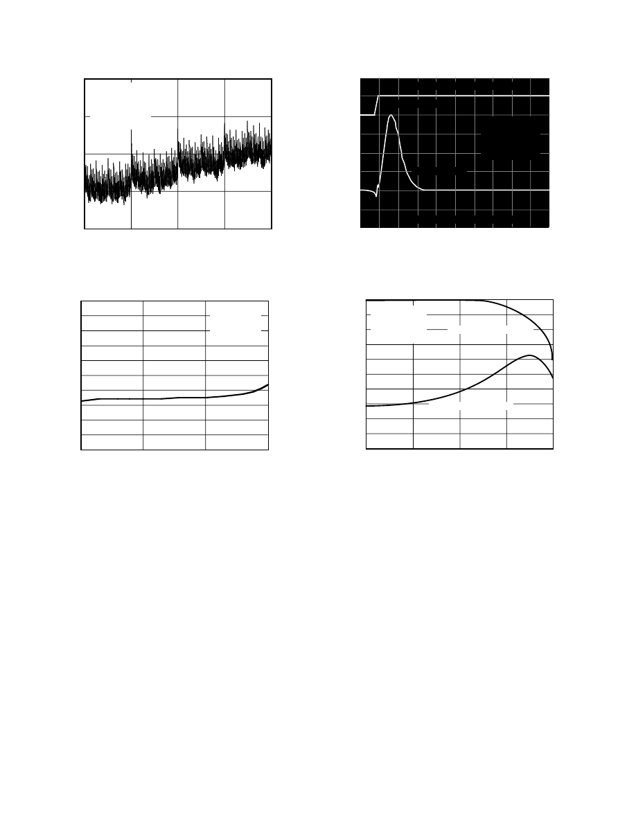
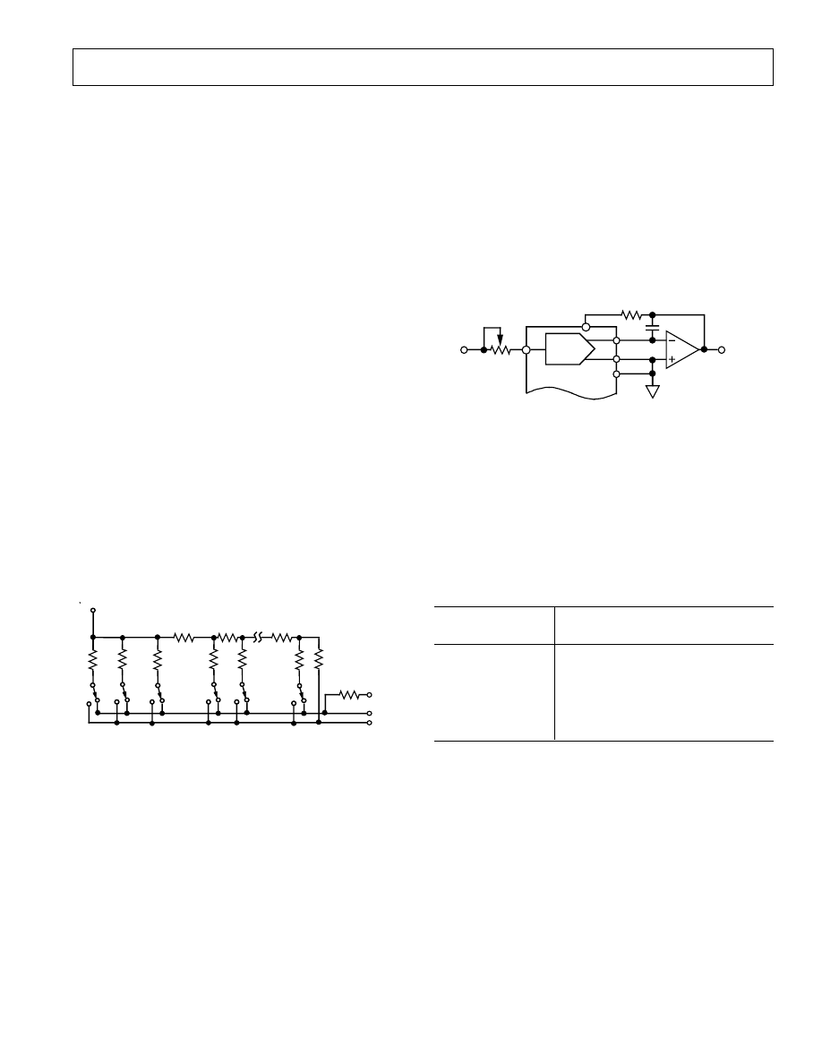
GENERAL DESCRIPTION
D/A Section
The AD7943, AD7945 and AD7948 are 12-bit current-output
D/A converters. A simplified circuit diagram is shown in Fig-
ure 13. The DAC architecture is segmented. This means that
the 2 MSBs of the 12-bit data word are decoded to drive the
three switches A, B and C. The remaining 10 bits of the data
word drive the switches S0 to S9 in a standard inverting R-2R
ladder configuration.
Each of the switches A to C steers 1/4 of the total reference cur-
rent into either I
OUT1
or I
OUT2
with the remaining 1/4 of the to-
tal current passing through the R-2R section. Switches S9 to S0
steer binarily weighted currents into either I
OUT1
or I
OUT2
. If
I
OUT1
and I
OUT2
are kept at the same potential, a constant cur-
rent flows in each ladder leg, regardless of digital input code.
Thus, the input resistance seen at V
REF
is always constant. It is
equal to R/2. The V
REF
input may be driven by any reference
voltage or current, ac or dc that is within the Absolute Maxi-
mum Ratings.
The device provides access to the V
REF
, R
FB
, and I
OUT1
termi-
nals of the DAC. This makes the device extremely versatile and
allows it to be configured in several different operating modes.
Examples of these are shown in the following sections. The
AD7943 also has a separate I
OUT2
pin. In the AD7945 and
AD7948 this is internally tied to AGND.
When an output amplifier is connected in the standard configu-
ration of Figure 14, the output voltage is given by:
V
OUT
= –D
×
V
REF
where D is the fractional representation of the digital word
loaded to the DAC. D can be set from 0 to 4095/4096, since it
has 12-bit resolution.
R
2R
2R
2R
R
FB
2R
2R
2R
R
R
SHOWN FOR ALL 1s ON DAC
2R
V
REF
R/2
C
B
A
S9
S8
S0
I
OUT1
I
OUT2
Figure 13. Simplified D/A Circuit Diagram
UNIPOLAR BINARY OPERATION
(Two-Quadrant Multiplication)
Figure 14 shows the standard unipolar binary connection dia-
gram for the AD7943, AD7945 and AD7948. When V
IN
is an
ac signal, the circuit performs two-quadrant multiplication. Re-
sistors R1 and R2 allow the user to adjust the DAC gain error.
With a specified gain error of 2 LSBs over temperature, these
are not necessary in many applications. Circuit offset is due
completely to the output amplifier offset. It can be removed by
adjusting the amplifier offset voltage. Alternatively, choosing a
low offset amplifier makes this unnecessary.
A1 should be chosen to suit the application. For example, the
OP07 is ideal for very low bandwidth applications (10 kHz or
I
OUT1
AGND
AD7943/45/48
DAC
V
REF
RFB
R1 20
Ω
R2 10
Ω
C1
A1
V
IN
V
OUT
NOTES
1. ONLY ONE DAC IS SHOWN FOR CLARITY.
2. DIGITAL INPUT CONNECTIONS ARE OMITTED.
3. C1 PHASE COMPENSATION (5–15pF) MAY BE REQUIRED WHEN
USING HIGH SPEED AMPLIFIER.
SIGNAL GROUND
I
OUT2
A1: OP07
AD711
AD843
AD845
Figure 14. Unipolar Binary Operation
lower) while the AD711 is suitable for medium bandwidth ap-
plications (200 kHz or lower). For high bandwidth applications
of greater than 200 kHz, the AD843 and AD847 offer very fast
settling times.
The code table for Figure 14 is shown in Table III.
Table III. Unipolar Binary Code
Digital Input
Analog Output
MSB LSB
(V
OUT
as Shown in Figure 15)
1111 1111 1111
–V
REF
(4095/4096)
1000 0000 0001
–V
REF
(2049/4096)
1000 0000 0000
–V
REF
(2048/4096)
0111 1111 1111
–V
REF
(2047/4096)
0000 0000 0001
–V
REF
(1/4096)
0000 0000 0000
–V
REF
(0/4096) = 0
NOTE
Nominal LSB size for the circuit of Figure 14 is given by: V
REF
(1/4096).
AD7943/AD7945/AD7948
REV. 0
–14–
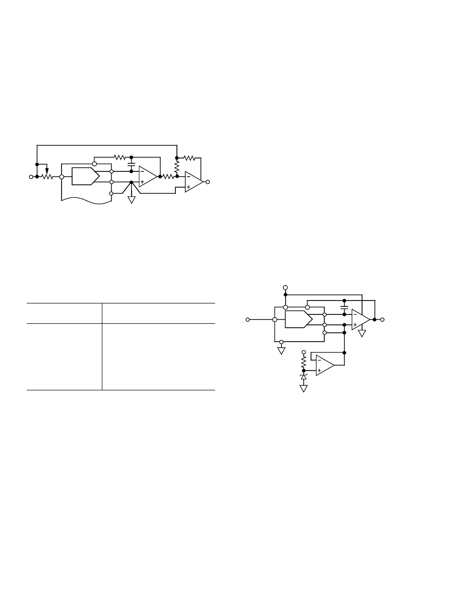
BIPOLAR OPERATION
(Four-Quadrant Multiplication)
Figure 15 shows the standard connection diagram for bipolar
operation of the AD7943, AD7945 and AD7948. The coding is
offset binary as shown in Table IV. When V
IN
is an ac signal,
the circuit performs four-quadrant multiplication. Resistors R1
and R2 are for gain error adjustment and are not needed in
many applications where the device gain error specifications are
adequate. To maintain the gain error specifications, resistors
R3, R4 and R5 should be ratio matched to 0.01%.
I
OUT1
AGND
AD7943/45/48
DAC
V
REF
RFB
R1 20
Ω
R2 10
Ω
C1
A1
V
IN
V
OUT
NOTES
1. ONLY ONE DAC IS SHOWN FOR CLARITY.
2. DIGITAL INPUT CONNECTIONS ARE OMITTED.
3. C1 PHASE COMPENSATION (5–15pF) MAY BE REQUIRED WHEN
USING HIGH SPEED AMPLIFIER, A1.
SIGNAL GROUND
A2
R3 10k
Ω
R4
20k
Ω
R5
20k
Ω
A2
I
OUT2
Figure 15. Bipolar Operation (Four-Quadrant
Multiplication)
Suitable dual amplifiers for use with Figure 15 are the OP270
(low noise, low bandwidth, 15 kHz), the AD712 (medium
bandwidth, 200 kHz) or the AD827 (wide bandwidth, 1 MHz).
Table IV. Bipolar (Offset Binary) Code
Table Digital Input
Analog Output
MSB LSB
(V
OUT
as Shown in Figure 16)
1111 1111 1111
+V
REF
(2047/2048)
1000 0000 0001
+V
REF
(1/2048)
1000 0000 0000
+V
REF
(0/2048) = 0
0111 1111 1111
–V
REF
(1/2048)
0000 0000 0001
–V
REF
(2047/2048)
0000 0000 0000
–V
REF
(2048/2048) = –V
REF
NOTE
Nominal LSB size for the circuit of Figure 15 is given by: V
REF
(1/2048).
SINGLE SUPPLY APPLICATIONS
The “-B” versions of the devices are specified and tested for
single supply applications. Figure 16 shows the recommended
circuit for operation with a single +5 V to +3.3 V supply. The
I
OUT2
and AGND terminals are biased to 1.23 V. Thus, with 0 V
applied to the V
REF
terminal, the output will go from 1.23 V (all
0s loaded to the DAC) to 2.46 V (all 1s loaded). With 2.45 V
applied to the V
REF
terminal, the output will go from 1.23 V (all
0s loaded) to 0.01 V (all 1s loaded). It is important when con-
sidering INL in a single-supply system to realize that most
single-supply amplifiers cannot sink current and maintain zero
volts at the output. In Figure 16, with V
REF
= 2.45 V the re-
quired sink current is 200
µ
A. The minimum output voltage
level is 10 mV. Op amps like the OP295 are capable of main-
taining this level while sinking 200
µ
A.
Figure 16 shows the I
OUT2
and AGND terminals being driven
by an amplifier. This is to maintain the bias voltage at 1.23 V
as the impedance seen looking into the I
OUT2
terminal changes.
This impedance is code dependent and varies from infinity (all
0s loaded in the DAC) to about 6 k
Ω
minimum. The AD589
has a typical output resistance of 0.6
Ω
and it can be used to
drive the terminals directly. However, this will cause a typical
linearity degradation of 0.2 LSBs. If this is unacceptable then
the buffer amplifier is necessary. Figure 9 shows the typical lin-
earity performance of the AD7943/AD7945/AD7948 when used
as in Figure 16 with V
DD
set at +3.3 V and V
REF
= 0 V.
I
OUT1
AGND
AD7943/45/48
DAC
V
REF
RFB
C1
A1
V
IN
V
OUT
I
OUT2
A1: OP295
AD822
OP283
DGND
A1
SIGNAL GROUND
+5V
5.6k
Ω
AD589
+3.3V
V
DD
Figure 16. Single Supply System
AD7943/AD7945/AD7948
REV. 0
–15–
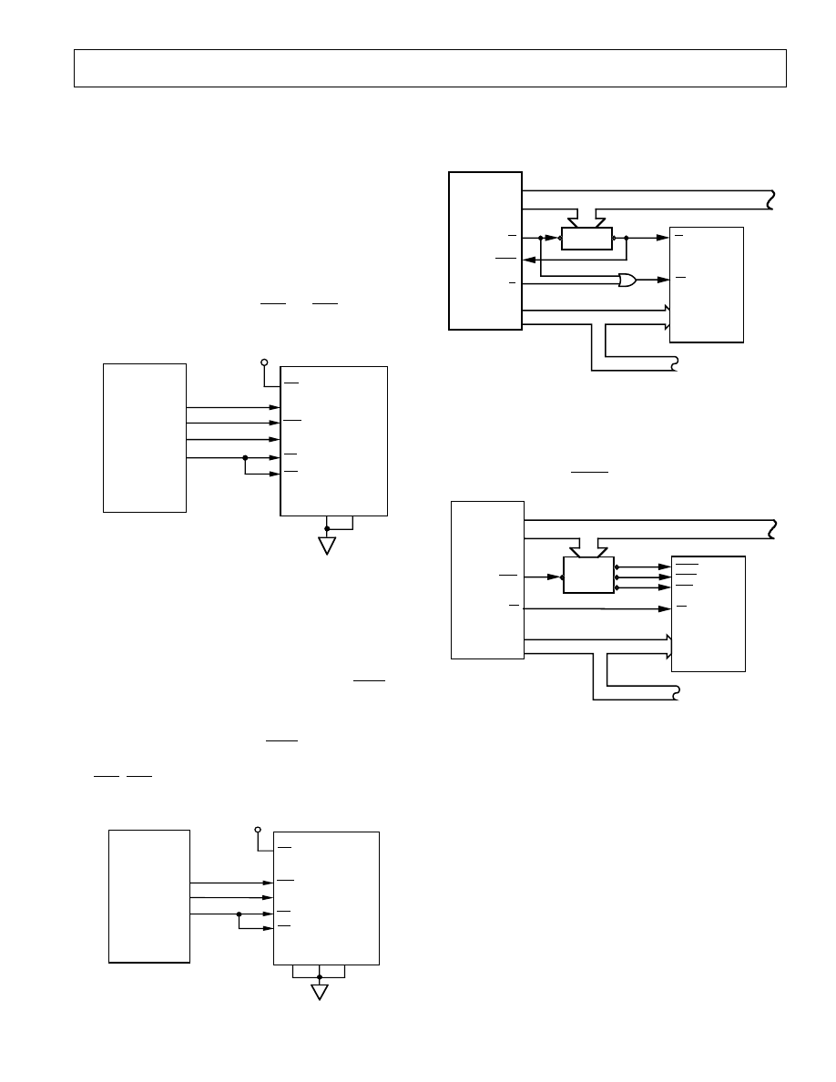
MICROPROCESSOR INTERFACING
AD7943 to ADSP-2101 Interface
Figure 17 shows the AD7943 to ADSP-2101 interface diagram.
The DSP is set up for alternate inverted framing with an inter-
nally generated SCLK. TFS from the ADSP-2101 drives the
STB1 input on the AD7943. The serial word length should be
set at 12. This is done by making SLEN = 11 (1011 binary).
The SLEN field is Bits 3–0 in the SPORT control register
(0x3FF6 for SPORT0 and 0x3FF2 for SPORT1).
With the 16 MHz version of the ADSP-2101, the maximum
output SCLK is 8 MHz. The AD7943 setup and hold time of
10 ns and 25 ns mean that it is compatible with the DSP when
running at this speed.
The OUTPUT FLAG drives both LD1 and LD2 and is brought
low to update the DAC register and change the analog output.
AD7943
ADSP-2101
CLR
OUTPUT FLAG
TFS
SCLK
DT
+5V
LD1
STB1
STB3
SRI
LD2
STB2
STB4
Figure 17. AD7943 to ADSO-2101 Interface
AD7943 to DSP56001 Interface
Figure 18 shows the interface diagram for the AD7943 to the
DSP56001. The DSP56001 is configured for normal mode syn-
chronous operation with gated clock. The serial clock, SCK, is
set up as an output from the DSP and the serial word length is
set for 12 bits (WL0 = 1, WL1 = 0, in Control Register A).
SCK from the DSP56001 is applied to the AD7943 STB3 in-
put. Data from the DSP56000 is valid on the falling edge of
SCK and this is the edge which clocks the data into the AD7943
shift register. STB1, STB2 and STB4 are tied low on the
AD7943 to permanently enable the STB3 input.
When the 12-bit serial word has been written to the AD7943,
the LD1, LD2 inputs are brought low to update the DAC
register.
AD7943
DSP56001
CLR
OUTPUT FLAG
SCK
STD
+5V
LD1
STB1
STB3
SRI
LD2
STB2
STB4
Figure 18. AD7943 to DSP56001 Interface
AD7945 to MC68000 Interface
Figure 19 shows the MC68000 interface to the AD7945. The
appropriate data is written into the DAC in one MOVE instruc-
tion to the appropriate memory location.
AD7945
MC68000
D15 – D0
DTACK
R/
W
DB11 – DB0
WR
CS
ADDRESS
DECODE
AS
A1 – A23
Figure 19. AD7945 to MC68000 Interface
AD7948 to Z80 Interface
Figure 20 is the interface between the AD7948 and the 8-bit
bus of the Z80 processor. Three write operations are needed to
load the DAC. The first two load the MS byte and the LS byte
and the third brings the LDAC low to update the output.
AD7948
Z80
D7 – D0
WR
DB7 – DB0
WR
CSMSB
ADDRESS
DECODE
MREQ
A0 – A15
CSLSB
LDAC
DATA BUS
ADDRESS BUS
Figure 20. AD7948 to Z80 Interface
AD7943/AD7945/AD7948
REV. 0
–16–
PRINTED IN U.S.A.
C1901–18–5/94
OUTLINE DIMENSIONS
Dimensions shown in inches and (mm).
16-Pin Plastic DIP (N-16)
16-Pin SOP (R-16)
0.325 (8.25)
0.300 (7.62)
0.015 (0.381)
0.008 (0.204)
0.195 (4.95)
0.115 (2.93)
PIN 1
0.280 (7.11)
0.240 (6.10)
9
16
1
8
0.210
(5.33)
0.200 (5.05)
0.125 (3.18)
0.022 (0.558)
0.014 (0.356)
0.100
(2.54)
BSC
SEATING
PLANE
0.060 (1.52)
0.015 (0.38)
0.150
(3.81)
0.070 (1.77)
0.045 (1.15)
0.840 (21.33)
0.745 (18.93)
PIN 1
0.299 (7.60)
0.291 (7.40)
0.419 (10.65)
0.404 (10.26)
1
16
9
8
0.018 (0.46)
0.014 (0.36)
0.050
(1.27)
BSC
0.107 (2.72)
0.089 (2.26)
0.413 (10.50)
0.398 (10.10)
0.010 (0.25)
0.004 (0.10)
0.015 (0.38)
0.007 (1.18)
0.045 (1.15)
0.020 (0.50)
0.364 (9.246)
0.344 (8.738)
20-Pin Plastic DIP (N-20)
20-Pin Cerdip (Q-20)
0.280 (7.11)
0.240 (6.10)
1.060 (26.90)
0.925 (23.50)
0.022 (0.558)
0.014 (0.356)
0.100 (2.54)
BSC
0.160 (4.06)
0.115 (2.93)
0.060 (1.52)
0.015 (0.38)
0.130
(3.30)
MIN
0.070 (1.77)
0.045 (1.15)
0.015 (0.381)
0.008 (0.204)
0.195 (4.95)
0.115 (2.93)
0.325 (8.25)
0.300 (7.62)
PIN 1
10
1
11
20
0.210
(5.33)
MAX
SEATING
PLANE
0.320 (8.13)
0.290 (7.37)
0.015 (0.38)
0.008 (0.20)
15
°
0
°
0.005 (0.13) MIN
PIN 1
0.098 (2.49) MAX
0.310 (7.87)
0.220 (5.59)
10
11
1
20
1.060 (26.92) MAX
0.200
(5.08)
MAX
0.023 (0.58)
0.014 (0.36)
0.200 (5.08)
0.125 (3.18)
0.100
(2.54)
BSC
0.070 (1.78)
0.030 (0.76)
0.060 (1.52)
0.015 (0.38)
0.150
(3.81)
MIN
SEATING
PLANE
20-Pin SOP (R-20)
20-Pin SSOP (RS-20)
PIN 1
0.2992 (7.60)
0.2914 (7.40)
0.4193 (10.65)
0.3937 (10.00)
1
20
11
10
0.0125 (0.32)
0.0091 (0.23)
0.0500 (1.27)
0.0157 (0.40)
8
°
0
°
0.0291 (0.74)
0.0098 (0.25)
x 45
°
0.5118 (13.00)
0.4961 (12.60)
0.0192 (0.49)
0.0138 (0.35)
0.0500
(1.27)
BSC
0.0118 (0.30)
0.0040 (0.10)
0.1043 (2.65)
0.0926 (2.35)
1. LEAD NO. 1 IDENTIFIED BY A DOT.
0.009 (0.229)
0.005 (0.127)
0.037 (0.94)
0.022 (0.559)
8
°
0
°
0.0256 (0.65)
BSC
0.07 (1.78)
0.066 (1.67)
0.295 (7.50)
0.271 (6.90)
0.008 (0.203)
0.002 (0.050)
PIN 1
0.311 (7.9)
0.301 (7.64)
0.212 (5.38)
0.205 (5.207)
1
20
11
10
Wyszukiwarka
Podobne podstrony:
7948
7945
7948
7948
7945
7948
7945
ad7943 id 51135 Nieznany
7945
7948
praca-magisterska-wa-c-7948, Dokumenty(2)
7945
praca-magisterska-wa-c-7945, Dokumenty(2)
7948
7945
7948
7945
7948
więcej podobnych podstron