
952
IEEE ELECTRON DEVICE LETTERS, VOL. 29, NO. 8, AUGUST 2008
Nonvolatile Switching in Graphene
Field-Effect Devices
Tim J. Echtermeyer, Max C. Lemme, Senior Member, IEEE, Matthias Baus,
Bartholomäus N. Szafranek, Andre K. Geim, and Heinrich Kurz
Abstract—The absence of a band gap in graphene restricts
its straightforward application as a channel material in field-
effect transistors. In this letter, we report on a new approach to
engineer a band gap in graphene field-effect devices (FEDs) by
controlled structural modification of the graphene channel itself.
The conductance in the FEDs is switched between a conductive
“
ON
-state” and an insulating “
OFF
-state” with more than six
orders of magnitude difference in conductance. Above a critical
value of an electric field applied to the FED gate under certain
environmental conditions, a chemical modification takes place to
form insulating graphene derivatives. The effect can be reversed
by electrical fields of opposite polarity or short current pulses to
recover the initial state. These reversible switches could poten-
tially be applied to nonvolatile memories and novel neuromorphic
processing concepts.
Index Terms—Field-effect transistor (FET), graphene, memory,
MOSFET, nonvolatile, switch.
I. I
NTRODUCTION
G
RAPHENE has been demonstrated to possess remarkable
intrinsic electronic properties that include carrier mobili-
ties exceeding 200 000 cm
2
/V
· s and a micrometer-scale mean
free path at room temperature [1]–[3]. As a consequence, one of
the most interesting applications in nanoelectronics is based on
the use of graphene as a channel material for field-effect tran-
sistors (FETs) [4]–[10]. However, the minimum conductance
of macroscopic graphene even at the neutrality (Dirac) point,
where no carriers are nominally present, results in low I
on
/I
off
ratios by far insufficient for CMOS-type applications. Indeed,
the best ratio achieved to date with a top-gated graphene FET
at room temperature is only six [9]. A possible escape route is
the use of graphene nanoribbons (GNRs) narrower than 5 nm,
which, in theory, will have a band gap larger than 500 meV
[11], [12]. Very recently, these predictions have been verified
experimentally by either using random methods similar to typi-
cal carbon nanotube processes [13] or deliberately overetching
predefined structures [14]. Nonetheless, reliable top–down fab-
Manuscript received April 18, 2008; revised May 28, 2008. This work was
supported by the German Federal Ministry of Education and Research (BMBF)
under Contract NKNF 03X5508 (“ALEGRA”). The review of this letter was
arranged by Editor J. Cai.
T. J. Echtermeyer, M. C. Lemme, M. Baus, B. N. Szafranek, and H. Kurz are
with the Advanced Microelectronic Center Aachen (AMICA), AMO GmbH,
52074 Aachen, Germany (e-mail: echtermeyer@amo.de; lemme@amo.de;
baus@amo.de; szafranek@amo.de; kurz@amo.de).
A. K. Geim is with the Manchester Centre for Mesoscience and Nan-
otechnology, University of Manchester, M13 9PL Manchester, U.K. (e-mail:
geim@manchester.ac.uk).
Color versions of one or more of the figures in this letter are available online
at http://ieeexplore.ieee.org.
Digital Object Identifier 10.1109/LED.2008.2001179
rication of such structures is not possible even with state-of-the-
art nanolithography tools. The smallest GNR-FETs fabricated
with controlled top–down lithography demonstrated so far have
shown widths of
∼10 nm [1], [7], [15], with electrical data
available for
∼30-nm GNRs.
In this letter, we report on graphene-based switches in a FET
configuration that rely on field-induced chemical modification
of graphene’s crystalline structure. I
on
/I
off
ratios of over 10
6
are achieved in these field-effect devices (FEDs; we use this no-
tion to indicate a different operational mechanism with respect
to the conventional FETs) at room temperature.
II. E
XPERIMENT
The graphene FEDs have been fabricated by exfoliation of
graphite on top of a silicon substrate with 300 nm of silicon
dioxide (SiO
2
) [16]. A 20-nm layer of silicon oxide (SiO
x
) has
been evaporated on top of graphene as a top-gate dielectric, and
a 40-nm tungsten film has been sputtered as source, drain, and
top-gate electrodes (for details, see [4] and [8]). In a separate
experiment, a 20-nm SiO
2
dielectric has been deposited by
chemical vapor deposition (CVD) at 425
◦
C. A schematic and
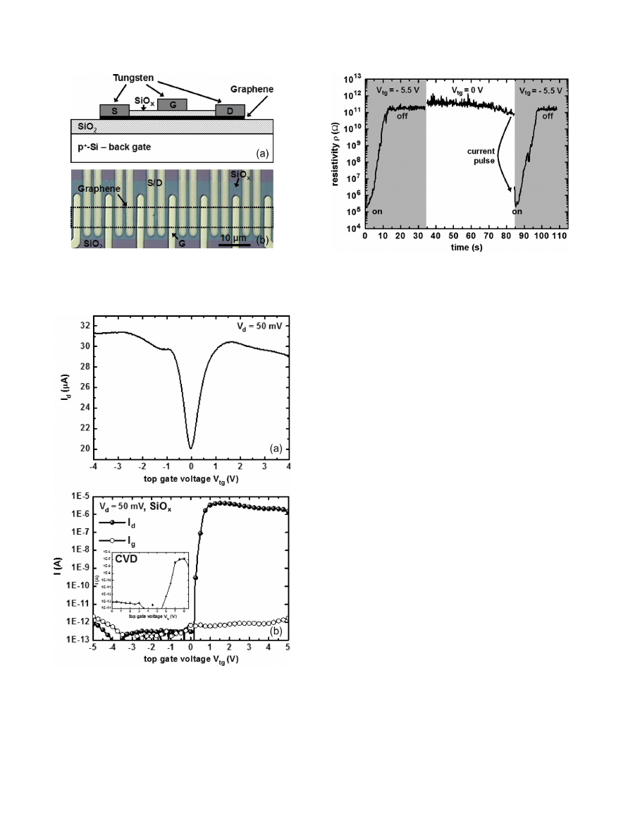
an optical micrograph of the devices are shown in Fig. 1(a)
and (b), respectively. An HP 4156 semiconductor parameter
analyzer has been used for electrical measurements. More
than ten samples have been fabricated, all of which exhibit the
switching effect described next.
III. R
ESULTS AND
D
ISCUSSION
Fig. 2(a) shows the top-gate transfer characteristic of a
graphene FED with 2-µm channel width and 4-µm gate length
measured in ambient conditions, with its Dirac point at V
g
=
0 V and, as expected, with a limited I
on
/I
off
ratio of
∼1.5. This
is a typical I
ds
/V
tg
characteristic of a graphene FET (compare,
e.g., [4]–[8], and [17]) and translates to a channel resistivity of
5 kΩ [labeled “
ON
-state” in Fig. 2(b)]. In this measurement,
the top-gate voltage has been swept back and forth between
V
tg
=
−4 V and V
tg
= 4 V, and the back-gate voltage has been
kept constant at V
bg
=
−40 V.
In a consecutive measurement, the range of the top-gate
voltage sweep has been extended above a certain critical value.
When starting the sweep at V
tg
=
−5 V, the drain current
drops by over seven orders of magnitude into an insulating
state of the proposed graphene FED (“
OFF
-state”). However,
this effect is reversible. As the voltage is swept starting from
V
tg
=
−5 V to V
tg
= 5 V (Fig. 2(b), filled circles), the device
remains insulating for negative voltages but recovers almost to
0741-3106/$25.00 © 2008 IEEE
Authorized licensed use limited to: The University of Manchester. Downloaded on July 28, 2009 at 04:52 from IEEE Xplore. Restrictions apply.
ECHTERMEYER et al.: NONVOLATILE SWITCHING IN GRAPHENE FIELD-EFFECT DEVICES
953
Fig. 1.
(a) Schematic of a double-gated graphene FED used in the experi-
ments. (b) Optical micrograph of several FEDs fabricated from one graphene
flake.
Fig. 2.
(a) Typical top-gate transfer characteristics of a graphene FED
with SiO
x
dielectric. (b) Top-gate transfer characteristics, including chemical
switching of the graphene FED with SiO
x
dielectric and gate leakage current.
Inset: Transfer characteristics of a device with CVD SiO
2
gate dielectric.
its initial
ON
-state current for V
tg
> 0 V. A low gate leakage
current excludes breakdown of the gate oxide as the responsible
mechanism (Fig. 2(b), hollow circles). The inset in Fig. 2(b)
shows the transfer characteristics of a device with a 20-nm CVD
SiO
2
, which exhibits the same qualitative switching behavior
even if a different dielectric is used.
Fig. 3.
Resistivity of a graphene FED over time, including three switching
events (on -> off -> on -> off).
The observed switching of the channel resistivity is attributed
to a chemical modification of the graphene, induced by the elec-
trostatic gate field. Two examples for such modified graphene
are graphane and graphene oxide. Graphane is a derivative
with hydrogen (H+) atoms attached in sp
3
configuration and
with a band gap of 3.5 eV [18]. Graphene oxide is a graphene
sheet with a large amount of hydroxyl (OH
−) or similar groups
attached to its surface, and it is insulating at room temperature
[19], [20]. We suggest that in our experiment, water from the
ambient or at the SiO
2
/graphene interface is split into H+ and
OH
−, which then attach to the graphene surface and open a
band gap. However, further experiments in this letter are aimed
at the application of the effect in a solid-state device, whereas
a detailed discussion of the underlying mechanisms and spe-
cific experiments, including dependences on the ambient (e.g.,
humidity and contaminants) and electrochemical gating, are
reported elsewhere [21].
Utilizing the observed switching effect in future electronic
applications obviously requires reliable ways of controlling
the switching and cycling it numerous times. Our approach
includes the field-induced switch-off, as shown in Fig. 2(b), but
it replaces the field-induced switch-on with short current pulses
of 80 µs in length (limited by the experimental setup). Fig. 3
shows a time-dependent measurement of the channel resistivity
of a graphene FED. The top- and back-gate voltages have
been kept constant at V
tg
=
−5.5 V and V
bg
= 0 V. Resistivity
increases by over six orders of magnitude to
∼5 × 10
11
Ω
and remains at this value. After reaching the
OFF
-state, a top-
gate voltage of V
tg
= 0 V has been applied, and the resistivity
remains in the
OFF
-state which shows the device’s nonvolatile
characteristic. Then, a current pulse of 50 µA has been applied
for 80 µs, after which the channel resistivity recovers fully.
Applying V
tg
=
−5.5 V has turned the device off again. While
the dc voltage compliance has been set to 8 V for the current
pulse, the actual ac voltage can be much higher but could not
be measured with the dc unit.
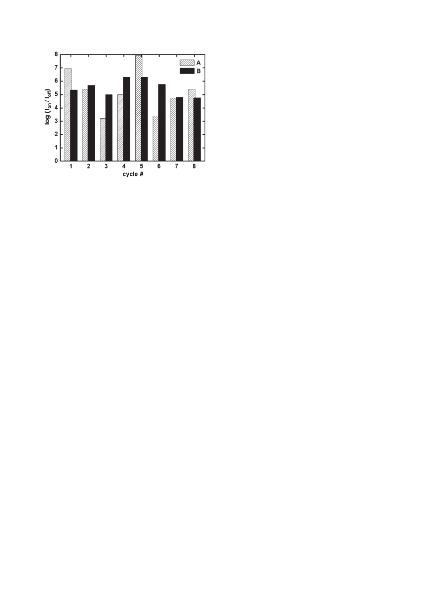
Fig. 4 shows the range of the resistivity change between
the
ON
- and
OFF
-states [log (I
on
/I
off
)] for two devices which
were both cycled eight times. Here, a top-gate voltage of V
tg
=
−4.5 V has been applied to turn off the devices, and single
Authorized licensed use limited to: The University of Manchester. Downloaded on July 28, 2009 at 04:52 from IEEE Xplore. Restrictions apply.
954
IEEE ELECTRON DEVICE LETTERS, VOL. 29, NO. 8, AUGUST 2008
Fig. 4.
Resistivity change in orders of magnitude for repeated switching from
the
ON
- to
OFF
-states of two graphene FEDs.
50-µA/80-µs current pulses have been used to restore the
ON
-state. Device A displays a spread in the modification of the
channel resistivity between three and eight orders of magnitude
compared with five to almost seven orders of magnitude in
device B. The observed spread can be interpreted as interme-
diate states of resistivity caused by different levels of chemical
modification of the graphene. In an additional experiment, a
device has been switched to the
OFF
-state and has then been left
in this condition in a clean room for two days, before returning
it to the
ON
-state with a standard current pulse. This hints
at reasonably large retention times of the effect. Even though
substantial further investigations are required to improve the
switching reliability and times and to identify potential storing
times and cyclability, our experiments clearly demonstrate the
potential of graphene FEDs as nonvolatile switches. In fact,
the observed resistivity changes of more than six orders of
magnitude are much larger than in “resistive” switches reported
recently [22]. In addition, multistage logic seems possible if
resistance values in graphene FEDs, as shown in Fig. 4, can
be controlled reliably.
IV. C
ONCLUSION
In this letter, we have reported on the modification of channel
resistivity in a graphene FED by over six orders of magni-
tude. The general device structure is identical to conventional
silicon-on-insulator and graphene MOSFETs, and the devices
may potentially be seen as candidates for future nonvolatile
memory applications. Our experiments show good cyclability
and reset times of 80 µs. Better understanding of the involved
processes should lead to improvements in switching times and
reliability in the future, including finding a reliable source for
the species involved in the switching mechanism. In the long
run, the observed intermediate states with ample margins may
be applicable to neuromorphic processors and networks.
A
CKNOWLEDGMENT
The authors would like to thank J. Bolten and T. Wahlbrink
for their e-beam lithography support.
R
EFERENCES
[1] S. V. Morozov, K. S. Novoselov, M. I. Katsnelson, F. Schedin,
D. C. Elias, J. A. Jaszczak, and A. K. Geim, “Giant intrinsic carrier
mobilities in graphene and its bilayer,” Phys. Rev. Lett., vol. 100, no. 1,
p. 016 602, Jan. 2008.
[2] J.-H. Chen, C. Jang, S. Xiao, M. Ishigami, and M. S. Fuhrer, “Intrinsic
and extrinsic performance limits of graphene devices on SiO2,” Nat.
Nanotech., vol. 3, pp. 206–209, 2008.
[3] K. I. Bolotin, K. J. Sikes, Z. Ziang, G. Fudenberg, J. Hone, P. Kim, and
H. L. Stormer, “Ultrahigh electron mobility in suspended graphene,” Solid
State Commun., vol. 146, no. 9/10, pp. 351–355, Jun. 2008.
[4] M. C. Lemme, T. J. Echtermeyer, M. Baus, and H. Kurz, “A graphene
field-effect device,” IEEE Electron Device Lett., vol. 28, no. 4, pp. 282–
284, Apr. 2007.
[5] B. Huard, J. A. Sulpizio, N. Stander, K. Todd, B. Yang, and
D. Goldhaber-Gordon, “Transport measurements across a tunable poten-
tial barrier in graphene,” Phys. Rev. Lett., vol. 98, no. 23, p. 236 803,
Jun. 2007.
[6] J. R. Williams, L. DiCarlo, and C. M. Marcus, “Quantum hall effect in
a gate-controlled p-n junction of graphene,” Science, vol. 317, no. 5838,
p. 638, Aug. 2007.
[7] B. Özyilmaz, P. Jarillo-Herrero, D. Efetov, D. A. Abanin, L. S. Levitov,
and P. Kim, “Electronic transport and quantum hall effect in bipolar
graphene p-n-p junctions,” Phys. Rev. Lett., vol. 99, no. 16, p. 166 804,
Oct. 2007.
[8] M. C. Lemme, T. J. Echtermeyer, M. Baus, and H. Kurz, “Mobility in
graphene double gate transistors,” Solid State Electron., vol. 52, no. 4,
pp. 513–517, Apr. 2008.
[9] A. Das, S. Pisana, B. Chakraborty, S. Piscanec, S. K. Saha,
U. V. Waghmare, K. S. Novoselov, H. R. Krishnamurthy, A. K. Geim,
A. C. Ferrari, and A. K. Sood, “Monitoring dopants by Raman scattering
in an electrochemically top-gated graphene transistor,” Nat. Nanotech.,
vol. 3, p. 10, Apr. 2008.
[10] J. Kedzierski, P.-L. Hsu, P. Healey, P. W. Wyatt, C. L. Keast, M. Sprinkle,
C. Berger, and W. A. de Heer, “Epitaxial graphene transistors on SiC
substrates,” IEEE Trans. Electron Devices, vol. 55, no. 8, pp. 2078–2085,
Aug. 2008.
[11] G. Fiori and G. Iannaccone, “Simulation of graphene nanoribbon field-
effect transistors,” IEEE Electron Device Lett., vol. 28, no. 8, pp. 760–762,
Aug. 2007.
[12] G. Liang, N. Neophytou, D. E. Nikonov, and M. S. Lundstrom, “Per-
formance projections for ballistic graphene nanoribbon field-effect tran-
sistors,” IEEE Trans. Electron Devices, vol. 54, no. 4, pp. 677–682,
Apr. 2007.
[13] X. Li, X. Wang, L. Zhang, S. Lee, and H. Dai, “Chemically derived,
ultrasmooth graphene nanoribbon semiconductors,” Science, vol. 319,
no. 5867, pp. 1229–1232, Feb. 2008.
[14] L. A. Ponomarenko, F. Schedin, M. I. Katsnelson, R. Yang, E. W.
Hill, K. S. Novoselov, and A. K. Geim, “Chaotic Dirac billiard in
graphene quantum dots,” Science, vol. 320, no. 5874, pp. 356–358,
Apr. 2008.
[15] P. Avouris, Z. Chen, and V. Perebeinos, “Carbon-based electronics,” Nat.
Nanotechnol., vol. 2, p. 605, Oct. 2007.
[16] K. S. Novoselov, A. K. Geim, S. V. Morozov, D. Jiang, Y. Zhang,
S. V. Dubonos, I. V. Grigorieva, and A. A. Firsov, “Electric field effect in
atomically thin carbon films,” Science, vol. 306, no. 5696, pp. 666–669,
Oct. 2004.
[17] Y. Q. Wu, P. D. Ye, M. A. Capano, Y. Xuan, Y. Sui, M. Qi, J. A. Cooper,
T. Shen, D. Pandey, G. Prakash, and R. Reifenberger, “Top-gated
graphene field-effect transistor formed by decomposition of SiC,” Appl.
Phys. Lett., vol. 92, no. 9, pp. 092 102-1–092 102-3, Mar. 2008.
[18] J. O. Sofo, A. S. Chaudhari, and G. D. Barber, “Graphane: A two-
dimensional hydrocarbon,” Phys. Rev. B, Condens. Matter, vol. 75, no. 15,
p. 153 401, Apr. 2007.
[19] C. Gómez-Navarro, R. T. Weitz, A. M. Bittner, M. Scolari, A. Mews,
M. Burghard, and K. Kern, “Electronic transport properties of individual
chemical reduced graphene oxide sheets,” Nano Lett., vol. 7, no. 11,
p. 3499, Sep. 2007.
[20] S. Gilje, S. Han, M. Wang, K. L. Wang, and R. B. Kaner, “A chemical
route to graphene for device applications,” Nano Lett., vol. 7, no. 11,
p. 3394, Sep. 2007.
[21] T. J. Echtermeyer, M. C. Lemme, M. Baus, B. N. Szafranek,
A. K. Geim, and H. Kurz, A Graphene-Based Electrochemical Switch.
arXiv:0712.2026v1.
[22] M. Wuttig and N. Yamada, “Phase-change materials for rewriteable data
storage,” Nat. Mater., vol. 6, pp. 824–832, Nov. 2007.
Authorized licensed use limited to: The University of Manchester. Downloaded on July 28, 2009 at 04:52 from IEEE Xplore. Restrictions apply.
Wyszukiwarka
Podobne podstrony:
kp, ART 241(13) KP, III PZP 1/08 - z dnia 15 października 2008 r
Rozwiązanie zadania z fizyki 5 13 Mroszczyk Salach dla szkół ponadgimnazjalnych cz1 ZamKor 2008
Rozwiązanie zadania z fizyki 6 13 Mroszczyk Salach dla szkół ponadgimnazjalnych cz1 ZamKor 2008
Rozwiązanie zadania z fizyki 4 13 Mroszczyk Salach dla szkół ponadgimnazjalnych cz1 ZamKor 2008
Rozwiązanie zadania z fizyki 0 13 Mroszczyk Salach dla szkół ponadgimnazjalnych cz1 ZamKor 2008
Rozwiązanie zadania z fizyki 1 13 Mroszczyk Salach dla szkół ponadgimnazjalnych cz1 ZamKor 2008
integracja 29.10.13, Ekonomia UP Lublin, EIE
Onkologia - zaliczenie (29.05.2008 - 13;00), Onkologia
29 Wzór nr 13
TPL PRAC 13 11 29 Proszki
wyklad 12 15.05.2008 i 13 29.05.2008, Administracja UŁ, Administracja I rok, Ustrój organów ochron
post przew modele TM od 29 03 13
ODL I sem termin1 13 01 29
TPL WYK 13 11 29 Proszki
Zad 13(29 06 2009)
13 (29)
więcej podobnych podstron