November 1995
2N7000 / 2N7002 / NDS7002A
N-Channel Enhancement Mode Field Effect Transistor
General Description
Features
___________________________________________________________________________________________
Absolute Maximum Ratings
T
A
= 25°C unless otherwise noted
Symbol
Parameter
2N7000
2N7002
NDS7002A
Units
V
DSS
Drain-Source Voltage
60
V
V
DGR
Drain-Gate Voltage (R
GS
< 1 M
Ω
)
60
V
V
GSS
Gate-Source Voltage - Continuous
±
20
V
- Non Repetitive (tp < 50µs)
±
40
I
D
Maximum Drain Current - Continuous
200
115
280
mA
- Pulsed
500
800
1500
P
D
Maximum Power Dissipation
400
200
300
mW
Derated above 25
o
C
3.2
1.6
2.4
mW/°C
T
J
,T
STG
Operating and Storage Temperature Range
-55 to 150
-65 to 150
°C
T
L
Maximum Lead Temperature for Soldering
Purposes, 1/16" from Case for 10 Seconds
300
°C
THERMAL CHARACTERISTICS
R
θ
JA
Thermal Resistance, Junction-to-Ambient
312.5
625
417
°C/W
2N7000.SAM Rev. A1
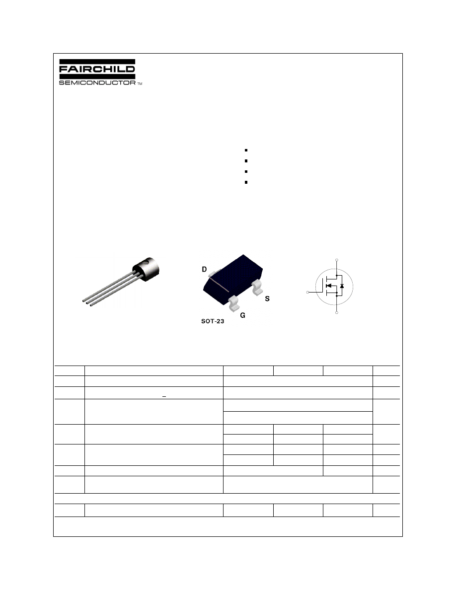
These N-Channel enhancement mode field effect transistors
are produced using Fairchild's proprietary, high cell density,
DMOS technology. These products have been designed to
minimize on-state resistance while provide rugged, reliable,
and fast switching performance. They can be used in most
applications requiring up to 400mA DC and can deliver
pulsed currents up to 2A. These products are particularly
suited for low voltage, low current applications such as small
servo motor control, power MOSFET gate drivers, and other
switching applications.
High density cell design for low R
DS(ON)
.
Voltage controlled small signal switch.
Rugged and reliable.
High saturation current capability.
S
D
G
S
G
D
TO-92
© 1997 Fairchild Semiconductor Corporation
2N7000
(TO-236AB)
2N7002/NDS7002A
Electrical Characteristics
T
A
= 25°C unless otherwise noted
Symbol
Parameter
Conditions
Typ
e
Min
Typ
Max
Units
OFF CHARACTERISTICS
BV
DSS
Drain-Source Breakdown Voltage
V
GS
= 0 V, I
D
= 10 µA
All
60
V
I
DSS
Zero Gate Voltage Drain Current
V
DS
= 48 V, V
GS
= 0 V
2N7000
1
µA
T
J
=125°C
1
mA
V
DS
= 60 V, V
GS
= 0 V
2N7002
NDS7002A
1
µA
T
J
=125°C
0.5
mA
I
GSSF
Gate - Body Leakage, Forward
V
GS
= 15 V, V
DS
= 0 V
2N7000
10
nA
V
GS
= 20 V, V
DS
= 0 V
2N7002
NDS7002A
100
nA
I
GSSR
Gate - Body Leakage, Reverse
V
GS
= -15 V, V
DS
= 0 V
2N7000
-10
nA
V
GS
= -20 V, V
DS
= 0 V
2N7002
NDS7002A
-100
nA
ON CHARACTERISTICS
(Note 1)
V
GS(th)
Gate Threshold Voltage
V
DS
= V
GS
, I
D
= 1 mA
2N7000
0.8
2.1
3
V
V
DS
= V
GS
, I
D
= 250 µA
2N7002
NDS7002A
1
2.1
2.5
R
DS(ON)
Static Drain-Source On-Resistance V
GS
= 10 V, I
D
= 500 mA
2N7000
1.2
5
Ω
T
J
=125°C
1.9
9
V
GS
= 4.5 V, I
D
= 75 mA
1.8
5.3
V
GS
= 10 V, I
D
= 500 mA
2N7002
1.2
7.5
T
J
=100°C
1.7
13.5
V
GS
= 5.0 V, I
D
= 50 mA
1.7
7.5
T
J
=100C
2.4
13.5
V
GS
= 10 V, I
D
= 500 mA
NDS7002
A
1.2
2
T
J
=125°C
2
3.5
V
GS
= 5.0 V, I
D
= 50 mA
1.7
3
T
J
=125°C
2.8
5
V
DS(ON)
Drain-Source On-Voltage
V
GS
= 10 V, I
D
= 500 mA
2N7000
0.6
2.5
V
V
GS
= 4.5 V, I
D
= 75 mA
0.14
0.4
V
GS
= 10 V, I
D
= 500mA
2N7002
0.6
3.75
V
GS
= 5.0 V, I
D
= 50 mA
0.09
1.5
V
GS
= 10 V, I
D
= 500mA
NDS7002A
0.6
1
V
GS
= 5.0 V, I
D
= 50 mA
0.09
0.15
2N7000.SAM Rev. A1
Electrical Characteristics
T
A
= 25
o
C unless otherwise noted
Symbol
Parameter
Conditions
Typ
e
Min
Typ
Max
Units
ON CHARACTERISTICS
Continued
(Note 1)
I
D(ON)
On-State Drain Current
V
GS
= 4.5 V, V
DS
= 10 V
2N7000
75
600
mA
V
GS
= 10 V, V
DS
> 2 V
DS(on)
2N7002
500
2700
V
GS
= 10 V, V
DS
> 2 V
DS(on)
NDS7002A
500
2700
g
FS
Forward Transconductance
V
DS
= 10 V, I
D
= 200 mA
2N7000
100
320
mS
V
DS
> 2 V
DS(on)
, I
D
= 200 mA
2N7002
80
320
V
DS
> 2 V
DS(on)
, I
D
= 200 mA
NDS7002A
80
320
DYNAMIC CHARACTERISTICS
C
iss
Input Capacitance
V
DS
= 25 V, V
GS
= 0 V,
f = 1.0 MHz
All
20
50
pF
C
oss
Output Capacitance
All
11
25
pF
C
rss
Reverse Transfer Capacitance
All
4
5
pF
t
on
Turn-On Time
V
DD
= 15 V, R
L
= 25
Ω
,
I
D
= 500 mA, V
GS
= 10 V,
R
GEN
= 25
2N7000
10
ns
V
DD
= 30 V, R
L
= 150
Ω
,
I
D
= 200 mA, V
GS
= 10 V,
R
GEN
= 25
Ω
2N700
NDS7002A
20
t
off
Turn-Off Time
V
DD
= 15 V, R
L
= 25
Ω
,
I
D
= 500 mA, V
GS
= 10 V,
R
GEN
= 25
2N7000
10
ns
V
DD
= 30 V, R
L
= 150
Ω
,
I
D
= 200 mA, V
GS
= 10 V,
R
GEN
= 25
Ω
2N700
NDS7002
A
20
DRAIN-SOURCE DIODE CHARACTERISTICS AND MAXIMUM RATINGS
I
S
Maximum Continuous Drain-Source Diode Forward Current
2N7002
115
mA
NDS7002A
280
I
SM
Maximum Pulsed Drain-Source Diode Forward Current
2N7002
0.8
A
NDS7002A
1.5
V
SD
Drain-Source Diode Forward
Voltage
V
GS
= 0 V, I
S
= 115 mA
(Note 1)
2N7002
0.88
1.5
V
V
GS
= 0 V, I
S
= 400 mA
(Note 1)
NDS7002
A
0.88
1.2
Note:
1. Pulse Test: Pulse Width < 300µs, Duty Cycle < 2.0%.
2N7000.SAM Rev. A1
2N7000.SAM Rev. A1
0
1
2
3
4
5
0
0 .5
1
1 .5
2
V , DRAIN-SOURCE VOLTAGE (V)
I , DR
A
IN-SOURCE CURRENT (A)
9.0
4.0
8.0
3.0
7.0
V = 10V
GS
DS
D
5.0
6.0
-5 0
-2 5
0
2 5
5 0
7 5
1 0 0
1 2 5
1 5 0
0 .5
0 .75
1
1 .25
1 .5
1 .75
2
T , JUNCTION T EMPERATURE (°C)
DRAI
N
-SOURCE ON-RESISTANCE
J
R ,
NO
R
MA
LIZED
DS(ON)
V = 10V
GS
I = 500m A
D
-50
-25
0
2 5
5 0
7 5
1 0 0
1 2 5
1 5 0
0 .8
0 .8 5
0 .9
0 .9 5
1
1 .0 5
1 .1
T , JUNCTION TEM PERA T U RE (°C)
GAT
E-SOURCE THRESHOLD VOLTAGE
J
I = 1 m A
D
V = V
DS
GS
V , NOR
MAL
IZED
th
0
0 .4
0 .8
1 .2
1 .6
2
0 .5
1
1 .5
2
2 .5
3
I , DRA IN CURRENT (A)
DRAI
N
-SOURCE ON-RESISTANCE
V =4.0V
GS
D
R ,
NO
RMALIZED
DS(on)
7 .0
4 .5
1 0
5 .0
6 .0
9 .0
8 .0
0
0 .4
0 .8
1 .2
1 .6
2
0
0 .5
1
1 .5
2
2 .5
3
I , DRAIN CURRENT (A)
DRAIN-SOURCE ON-RESISTANCE
T = 1 2 5 ° C
J
2 5 ° C
-55°C
D
V = 10V
GS
R ,
NO
RMALIZED
DS(on)
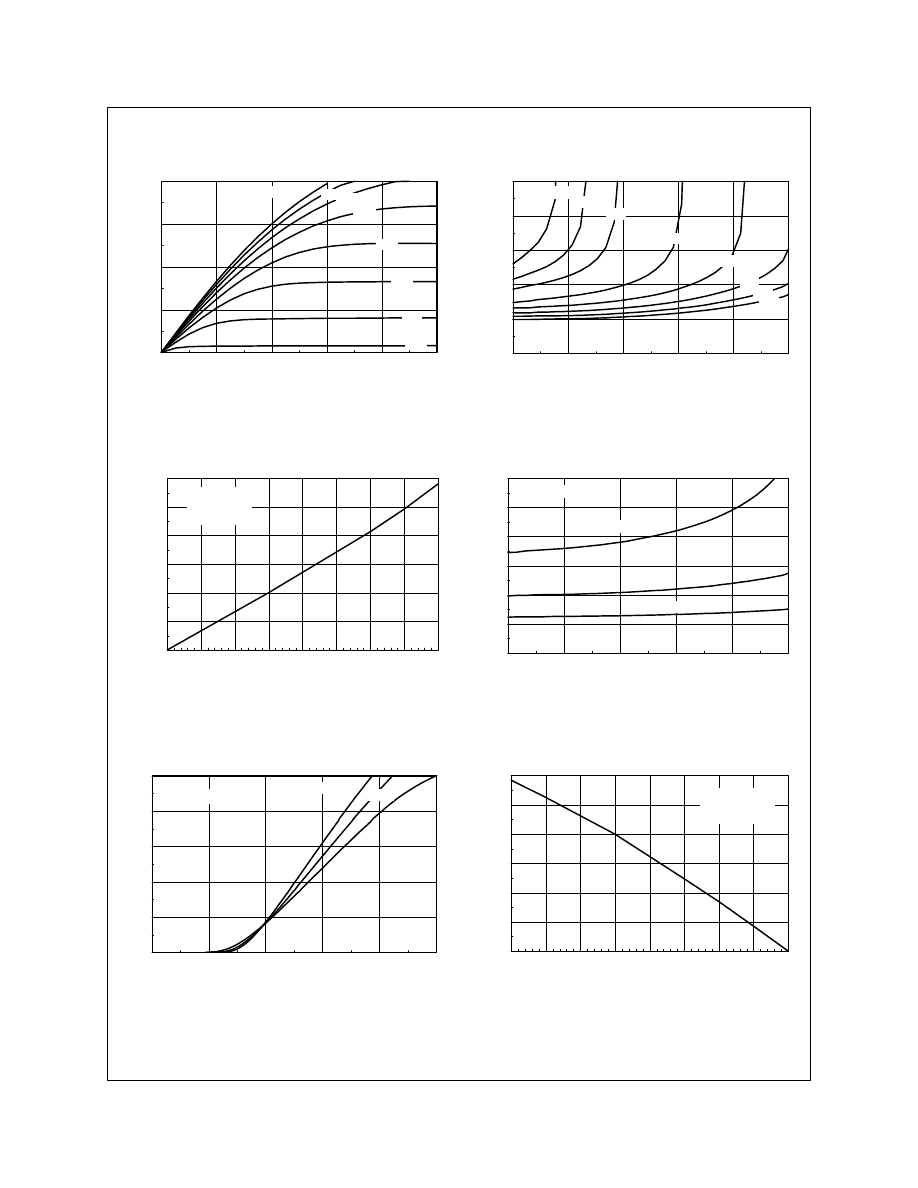
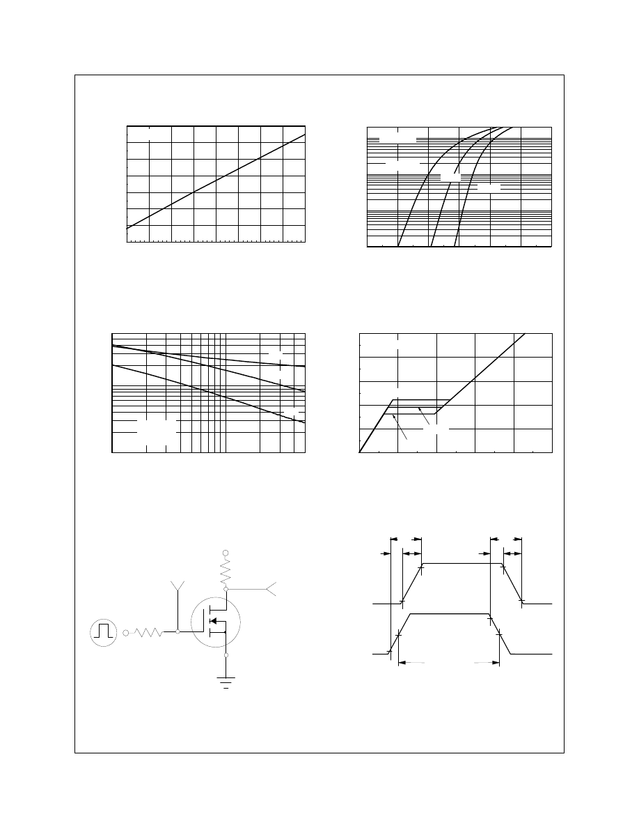
Typical Electrical Characteristics
Figure 1. On-Region Characteristics
Figure 2. On-Resistance Variation with Gate
Voltage and Drain Current
Figure 3. On-Resistance Variation
with Temperature
Figure 4. On-Resistance Variation with Drain
Current and Temperature
Figure 5. Transfer Characteristics
Figure 6. Gate Threshold Variation with
Temperature
0
2
4
6
8
10
0
0.4
0.8
1.2
1.6
2
V , GATE TO SOURCE VOLTAGE (V)
I , DR
A
IN CURRENT (A)
V = 1 0 V
DS
GS
D
T = -55°C
J
2 5 ° C
1 2 5 ° C
2N7000 / 2N7002 / NDS7002A
2N7000.SAM Rev. A1
-50
-25
0
2 5
5 0
7 5
1 0 0
1 2 5
1 5 0
0.925
0.95
0.975
1
1.025
1.05
1.075
1.1
T , JUNCTION TEM PERATURE (°C)
DRAIN-SOURCE BREAKDO
WN VOLTAG
E
J
BV , NORMALIZED
DSS
I = 250µA
D
0 .2
0 .4
0 .6
0 .8
1
1 .2
1 .4
0 .0 0 1
0 .0 0 5
0 .0 1
0 .0 5
0 .1
0 .5
1
2
V , BODY DIODE FORW A RD VOLTAGE (V)
I , REVERSE DR
A
IN CURRENT (A)
V = 0 V
GS
T = 1 2 5 ° C
J
SD
S
2 5 ° C
-5 5 ° C
0
0 .4
0 .8
1 .2
1 .6
2
0
2
4
6
8
1 0
Q , GATE CHARGE (nC)
V , GAT
E-SO
URCE VOLTAGE (V)
g
GS
I = 5 0 0 m A
D
V = 2 5 V
DS
1 1 5 m A
2 8 0 m A
1
2
3
5
1 0
2 0
3 0
5 0
1
2
5
1 0
2 0
4 0
6 0
V , DRAIN TO SOURCE VOLTAGE (V)
CAPACITANCE (pF)
DS
C
iss
f = 1 M H z
V = 0V
GS
C
oss
C
rss
G
D
S
V
DD
R
L
V
V
IN
OUT
V
GS
DUT
R
GEN
10%
50%
90%
10%
90%
90%
50%
Input, Vin
Output, Vout
t
on
t
off
t
d(off)
t
f
t
r
t
d(on)
Inverted
10%
Pulse Width
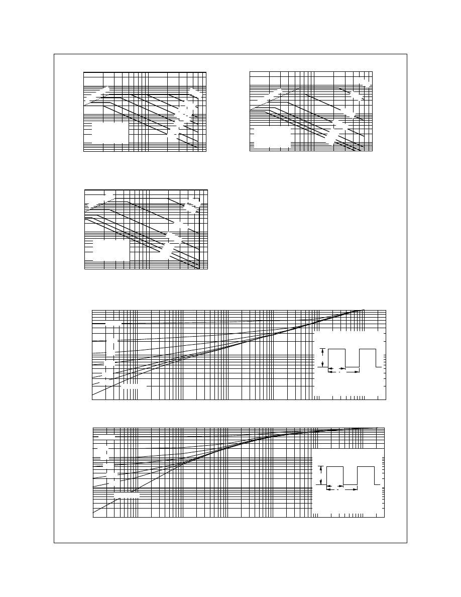
Figure 7. Breakdown Voltage Variation
with Temperature
Figure 8. Body Diode Forward Voltage Variation with
Figure 9. Capacitance Characteristics
Figure 10. Gate Charge Characteristics
Figure 11.
Figure 12. Switching Waveforms
Typical Electrical Characteristics
(continued)
2N7000 / 2N7002 /NDS7002A
2N7000.SAM Rev. A1
0.0001
0.001
0.01
0.1
1
10
100
300
0.001
0.002
0.01
0.05
0.1
0.2
0.5
1
t , TIME (sec)
T
R
A
N
S
IE
N
T
T
H
E
R
M
A
L
R
E
S
IS
T
A
N
C
E
r(t), NORMALIZED EFFECTIVE
1
Single Pulse
D = 0.5
0.1
0 .0 5
0 .0 2
0 .0 1
0 .2
Duty Cycle, D = t /t
1
2
R (t) = r(t) * R
R = (See Datasheet)
θ
JA
θ
JA
θ
JA
T - T = P * R (t)
θ
JA
A
J
P(pk)
t
1
t
2
0.0001
0.001
0.01
0.1
1
10
100
300
0.01
0.02
0.05
0.1
0.2
0.5
1
t , TIME (sec)
T
R
A
N
S
IE
N
T
T
H
E
R
M
A
L
R
E
S
IS
T
A
N
C
E
r(t), NORMALIZED EFFECTIVE
1
Single Pulse
D = 0 .5
0.1
0.05
0 .02
0.01
0 .2
Duty Cycle, D = t /t
1
2
R (t) = r(t) * R
R = (See Datasheet)
θ
JA
θ
JA
θ
JA
T - T = P * R (t)
θ
JA
A
J
P(pk)
t
1
t
2
1
2
5
1 0
2 0
3 0
6 0
8 0
0.005
0.01
0.05
0.1
0.5
1
2
3
V , DRAIN-SOURCE VOLTAGE (V)
I , DRAI
N
C
URRENT (A)
DS
D
V = 10V
SINGLE PULSE
T = 25°C
GS
A
RDS(ON) Li
m
it
100
m
s
1 m
s
10
m
s
DC
1s
100us
10
s
Figure 16. TO-92, 2N7000 Transient Thermal Response Curve
Figure 17. SOT-23, 2N7002 / NDS7002A Transient Thermal Response Curve
1
2
5
1 0
2 0
3 0
6 0
8 0
0.005
0.01
0.05
0.1
0.5
1
2
3
V , DRAIN-SOURCE VOLTAGE (V)
I , DRAI
N
C
URRENT (A)
DS
D
V = 10V
SINGLE PULSE
T = 25°C
GS
A
RDS(ON) Li
m
it
100
m
s
1 m
s
10
m
s
DC
1s
10
s
100us
1
2
5
1 0
2 0
3 0
6 0
8 0
0.005
0.01
0.05
0.1
0.5
1
2
3
V , DRAIN-SOURCE VOLTAGE (V)
I , DRAI
N
C
URRENT (A)
DS
D
V = 10V
SINGLE PULSE
T = 25°C
GS
A
RDS(ON) Li
m
it
100
m
s
1 m
s
10
m
s
DC
1 s
10
s
100us
Figure 13. 2N7000 Maximum
Safe Operating Area
Figure 14. 2N7002 Maximum
Safe Operating Area
Figure 15. NDS7000A Maximum
Safe Operating Area
Typical Electrical Characteristics
(continued)
TRADEMARKS
The following are registered and unregistered trademarks Fairchild Semiconductor owns or is authorized to use and is
not intended to be an exhaustive list of all such trademarks.
LIFE SUPPORT POLICY
FAIRCHILD’S PRODUCTS ARE NOT AUTHORIZED FOR USE AS CRITICAL COMPONENTS IN LIFE SUPPORT
DEVICES OR SYSTEMS WITHOUT THE EXPRESS WRITTEN APPROVAL OF FAIRCHILD SEMICONDUCTOR CORPORATION.
As used herein:
1. Life support devices or systems are devices or
systems which, (a) are intended for surgical implant into
the body, or (b) support or sustain life, or (c) whose
failure to perform when properly used in accordance
with instructions for use provided in the labeling, can be
reasonably expected to result in significant injury to the
user.
2. A critical component is any component of a life
support device or system whose failure to perform can
be reasonably expected to cause the failure of the life
support device or system, or to affect its safety or
effectiveness.
PRODUCT STATUS DEFINITIONS
Definition of Terms
Datasheet Identification
Product Status
Definition
Advance Information
Preliminary
No Identification Needed
Obsolete
This datasheet contains the design specifications for
product development. Specifications may change in
any manner without notice.
This datasheet contains preliminary data, and
supplementary data will be published at a later date.
Fairchild Semiconductor reserves the right to make
changes at any time without notice in order to improve
design.
This datasheet contains final specifications. Fairchild
Semiconductor reserves the right to make changes at
any time without notice in order to improve design.
This datasheet contains specifications on a product
that has been discontinued by Fairchild semiconductor.
The datasheet is printed for reference information only.
Formative or
In Design
First Production
Full Production
Not In Production
DISCLAIMER
FAIRCHILD SEMICONDUCTOR RESERVES THE RIGHT TO MAKE CHANGES WITHOUT FURTHER
NOTICE TO ANY PRODUCTS HEREIN TO IMPROVE RELIABILITY, FUNCTION OR DESIGN. FAIRCHILD
DOES NOT ASSUME ANY LIABILITY ARISING OUT OF THE APPLICATION OR USE OF ANY PRODUCT
OR CIRCUIT DESCRIBED HEREIN; NEITHER DOES IT CONVEY ANY LICENSE UNDER ITS PATENT
RIGHTS, NOR THE RIGHTS OF OTHERS.
PowerTrench
QFET™
QS™
QT Optoelectronics™
Quiet Series™
SILENT SWITCHER
SMART START™
SuperSOT™-3
SuperSOT™-6
SuperSOT™-8
FASTr™
GlobalOptoisolator™
GTO™
HiSeC™
ISOPLANAR™
MICROWIRE™
OPTOLOGIC™
OPTOPLANAR™
PACMAN™
POP™
Rev. G
ACEx™
Bottomless™
CoolFET™
CROSSVOLT™
DOME™
E
2
CMOS
TM
EnSigna
TM
FACT™
FACT Quiet Series™
FAST
SyncFET™
TinyLogic™
UHC™
VCX™
Wyszukiwarka
Podobne podstrony:
2N7002K (Fairchild Semiconductor)
MPSA65, MMBTA65, PZTA65 (Fairchild Semiconductor)
H11A817 (Fairchild Semiconductor)
PN2222A, MMBT2222A, PZT2222A (Fairchild Semiconductor)
2N546x, MMBF546x (Fairchild Semiconductor)
TMC1175 (Fairchild Semiconductor)
BCV27 (Fairchild Semiconductor)
2N3906, MMBT3906, PZT3906 (Fairchild Semiconductor)
FOD3120 (Fairchild Semiconductor)
FQPF17N40 (Fairchild Semiconductor)
TIP100, TIP101, TIP102 (Fairchild Semiconductor)
MJE2955T (Fairchild Semiconductor)
PN2222 (Fairchild Semiconductor)
BC327, BC328 (Fairchild Semiconductor)
FOD817 (Fairchild Semiconductor)
KSP94 (Fairchild Semiconductor)
więcej podobnych podstron