
1
E365 Trouble Shooting
Service Manual
Compal Communications, Inc.
2
△
Baseband Descriptions
1.
The mobile phone can’t boot after inserting the battery?
•STEP1. Check the energy of battery greater than 3.8v.(>3.8v)
a. to charge the battery. b. change the battery.
•STEP2. Check the battery connector
a. recombination. b.change the battery connector
•STEP3. Check the BTB connector between M/B and MMI
a. recombination
•STEP4. Check the MMI whether in normal
a. recombination
•STEP5. Check the software in correct
a. Re D/L
2.
The mobile phone turn off automatically after turn on?
•STEP 1.Check battery if voltage enough greater than(>3.8v)
a. recombination b. Change battery
•STEP 2.Check ADC(3.4v) is correct
a. Re-adjustment ADC(3.4v)
•STEP 3.IF above-mentioned are all in normal condition then the problem could be
caused by M/B.
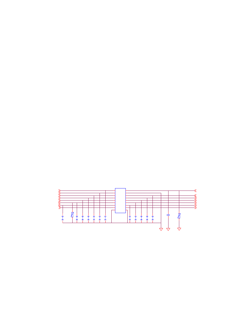
STEP3.1check J2.Row4 and GND maybe short.
STEP3.2.check J2 Pwon and GND maybe short.
VDDS-MIF_2.8V
LIGHTSENSER_EN
DGND
COL4
COL3
COL2
COL1
COL0
PWON
ROW0
DGND
DGND
J2
BTB_CON
1
2
3
4
5
6
7
15
16
14
13
12
11
10
8
9
17
18
GAP3
S
ROW3
ROW2
ROW4
LEDKEYN
VBAT
ROW1
VR3
varistor 5.5V 0402
C46
22pF 0402
GAP8
S
GAP14
S
GAP12
S
GAP10
S
GAP7
S
GAP9
S
GAP13
S
GAP11
S
GAP6
S
GAP5
S
GAP4
S
VR16
varistor 5.5V 0402
3.
The screen display can’t search SIM card when insert SIM after turn on.
•STEP 1.Check the SIM card whether to louse.
a. Change SIM card.
•STEP 2.Check the SIM connecter.
a. Change SIM connector.
•STEP 3.IF above-mentioned are all in normal condition then the problem could be
caused by M/B.
a. if change SIM connector isn’t ok,then change a new IOTA.
3
5.
No display on LCD after turn on?
•STEP 1.Check the connector of LCD and FPC
a. recombination
•STEP 2.Check the LCD whether to louse
a. Change LCD
•STEP 3.IF above-mentioned are all in normal condition then the problem could be
caused by M/B.
STEP 3.1.checkVDDS-MIF_2.8V =2.8V (if VRMEM<2.7V, the LCD will not
work)
STEP 3.2. check J6 every PIN’s impedance, then you can find one of them
has problem
6.
Has not LCM backlight :
•STEP 1. Check SET is correct
a. To set up LCD light bright mode.
•STEP 2. Check LCD and M/B whether to connect
a. Recombination.
•STEP 3. Check LCD failure
4
a. Change LCD.
•STEP 4.IF above-mentioned are all in normal condition then the problem could be
caused by M/B
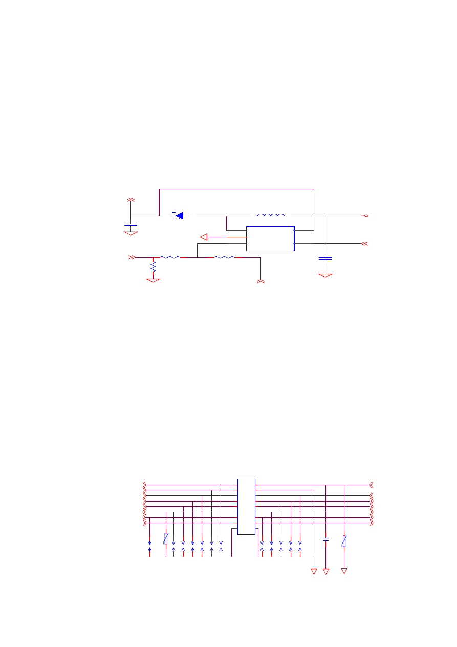
STEP 1.Check U11 is slant.
STEP 2. when you press the keypad ,measure U11.4=2.7V
STEP 3. if RR1 have about 0.4V,then change U11.
STEP 4.if U11.4 < 2.7V,then change a new G2.
STEP 5.if step1 to step4 is ok, then check U6.3 about 10V
STEP 6.if U11.1<8V ,then change a new U11 or FL1、D6.
.
U11
MP1523
SW
1
GND
2
FB
3
EN
4
BIAS
5
FL1
22uH
CC2
1uF 0603
R36
0 0402
R40
0 0402 NM
VDDS-MIF_2.8V
LED_Cathode
LEDLCM_EN
LED_Anode
VBAT
DGND
DGND
DGND
DGND
RR1
56 0402
D6
RB551V-30
2
3
CC1
0.22uF 0603
7.
Has not Keypad Backlight ?
•STEP 1 Check the BTB connector between M/B and MMI
a. Recombination
•STEP 2.Check MMI whether to have problem
a. Change MMI
•STEP 3.IF above-mentioned are all in normal condition then the problem could be
caused by M/B.
STEP3.1.use meter to check J2 every PIN impedance, then you can find
one of them has
problem.
VDDS-MIF_2.8V
LIGHTSENSER_EN
DGND
COL4
COL3
COL2
COL1
COL0
PWON
ROW0
DGND
DGND
J2
BTB_CON
1
2
3
4
5
6
7
15
16
14
13
12
11
10
8
9
17
18
GAP3
S
ROW3
ROW2
ROW4
LEDKEYN
VBAT
ROW1
VR3
varistor 5.5V 0402
C46
22pF 0402
GAP8
S
GAP14
S
GAP12
S
GAP10
S
GAP7
S
GAP9
S
GAP13
S
GAP11
S
GAP6
S
GAP5
S
GAP4
S
VR16
varistor 5.5V 0402
Step3.2 LEDKEY_EN= 1.4 ~ 2.8V, BQ3.pin3 = 1V DC
5
LEDK
E
KeyLed_En
LEDB
DGND
R64
0 0402 NM
R65
1.5K 0402
BQ3
2SC5585 EMT3
2
1
3
R67
1K 0402
C73
33nF 0402
R66
4.7 0402
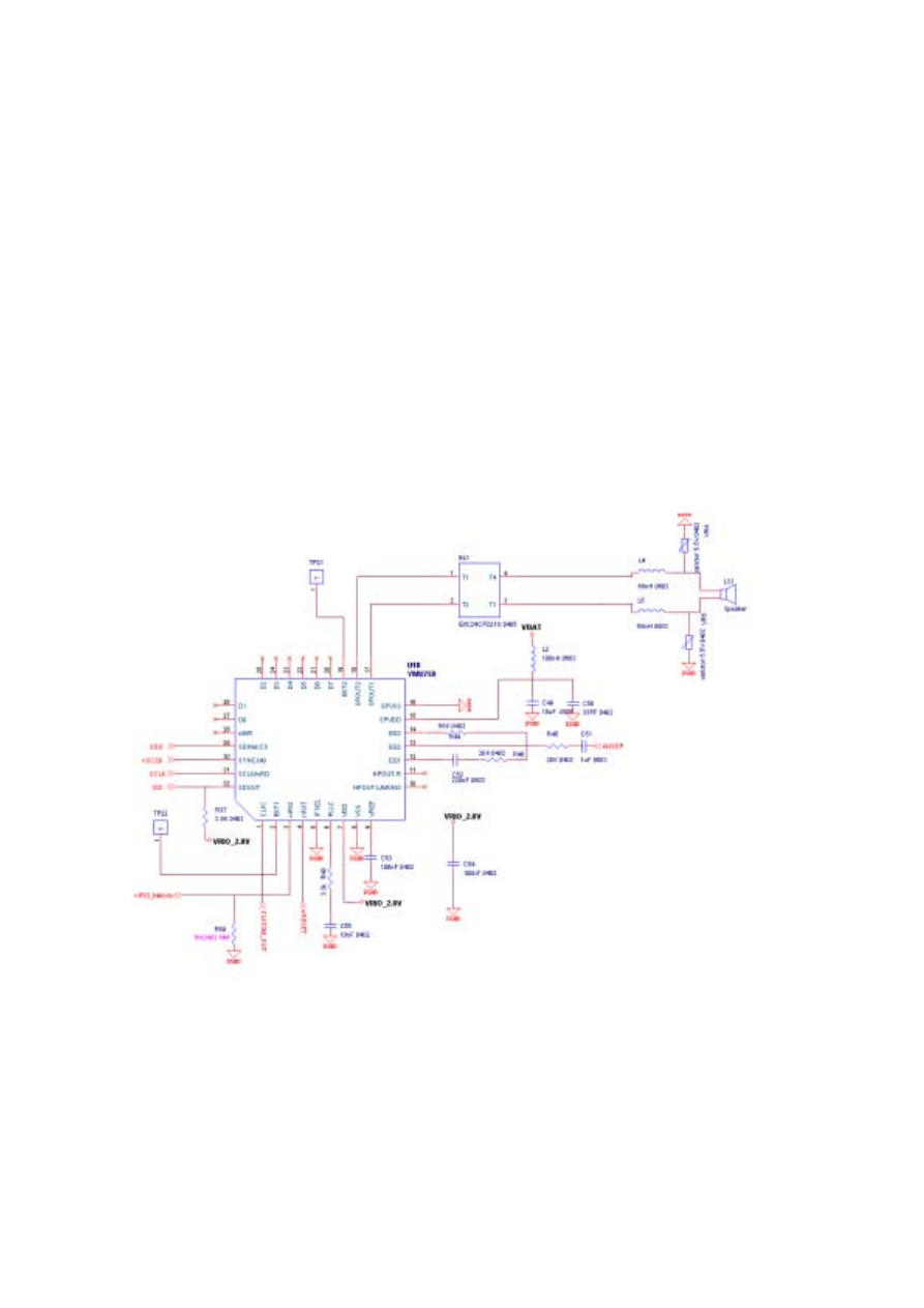
8.
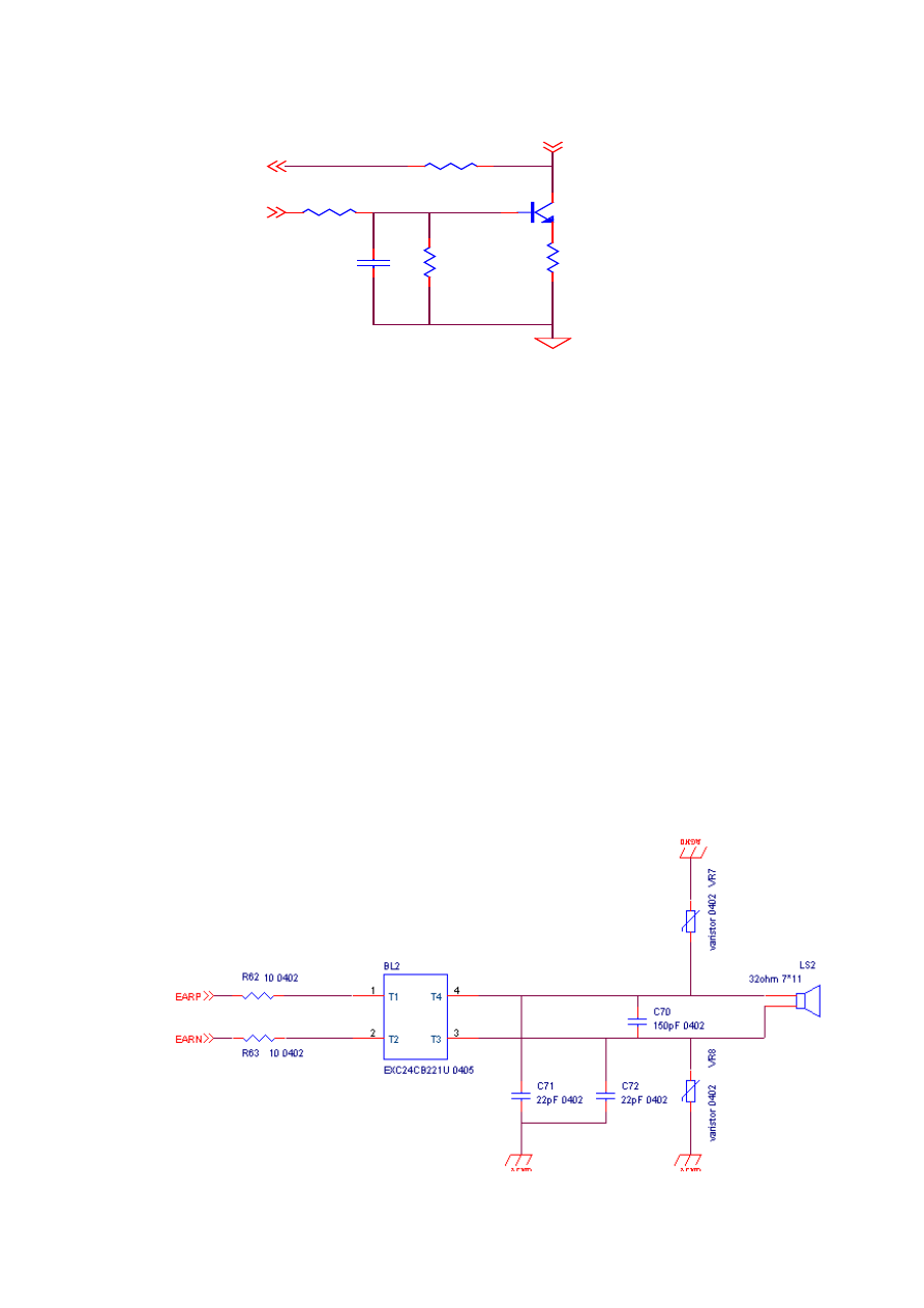
Receiver has no key tone or sound.
•STEP 1.Check SET is correct
a. set up to key tone mode.
•STEP 2.Check Receiver pin is that slanting or sag
a. To adjust the Receiver pin.
•STEP 3.Check Receiver whether in normal
a. Change Receiver.
•STEP 4.Check M/B pad is that oxidation or dirty
a. Use a eraser to clean the pad.
•STEP 5.IF above-mentioned are all in normal condition then the problem could be
caused by M/B
STEP 5.1.check every part impedance (R62、R63、C70、C71,C72、VR7、
VR8).
STEP 5.2.if every part is ok, then change a new IOTA.
6
9.
No ring tone
•STEP 1.Check SET is correct
a. Set up to ring mode.
•STEP 2.Check speaker hold has screwed
a. lock up a screw.
•STEP 3.Check speaker failure?
a. Change Speaker.
•STEP 4.Check speaker Connector damage?
a. Changed Speaker Connector.
•STEP 5.IF above-mentioned are all in normal condition then the problem could be
caused by M/B.
STEP5.1.check MELODY “Pin17、Pin18” impedance.
STEP5.2.if step1 is ok, measure L2, C49, C50, R45, R46,
R44,C51,C52,R37,C53,C54,C55,R48 impedance. Then
you can find one of them has problem.
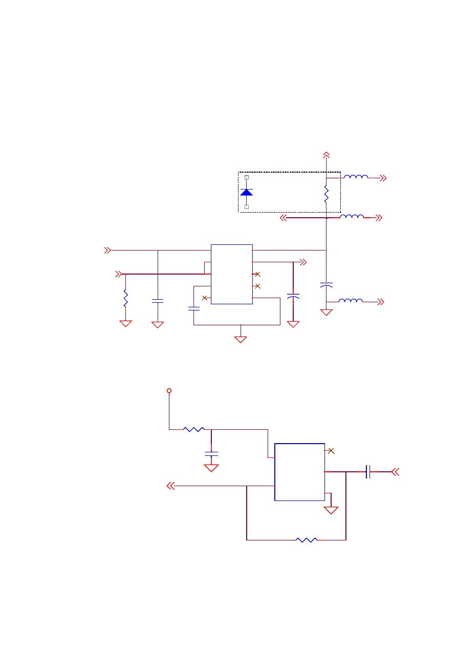
10. Can not charging:
•STEP 1.Check if you use the right adaptor
a. Change right adaptor.
•STEP 2.Check I/O Connector failure?
a. Change I/O Connector.
•STEP 3.Check I/O Connector Pin1&Pin2 solder creak?
a. I/O Connector Pin1&Pin2 re-soldering.
7
•STEP 4.IF above-mentioned are all in normal condition then the problem could be
caused by M/B. STEP 4.1.if U2.4 <5.8v,then change a new U2.
STEP 4.2.if step1 is ok, then change a new IOTA.
nCHG
C10
22nF 0402
R15 100K 0402
U3
NCP345
OUT
1
GND
2
CNTRL
3
IN
4
VCC
5
DGND
DGND
DGND
nCHG
VCHG1
ICTL
VCHG
PCHG
VBATS
VCCS
VBAT
R1
0.15 0805 1%
U2
FDC6506P
4
2
3
1
5
6
R5
68 0805 1% NM
C21
1uF 0603
D2
RB160M-30
2
3
11. Key has not function
•STEP 1. Check the BTB connector between M/B and MMI is well?
a. Recombination.
•STEP 2. Check MMI whether to have problem
a. Change MMI.
•STEP 3.Check MMI Pad whether to oxidize and dirty
a. Use a eraser to clean the pad.
•STEP 4. .IF above-mentioned are all in normal condition then the problem could
be caused by M/B.
STEP 4.1.check BTB connector is short.
STEP 4.2.if not short, then change a new G2
8
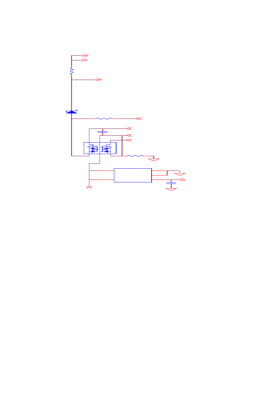
12. Has not vibration or vibrator can not stop.
•STEP 1.Check SET is correct
a. Set up to vibrate mode.
•STEP 2.Check Vibrator Pin is that slanting and sag
a. To adjust the Vibrator Pin.
•STEP 3. Check Vibrator failure?
a. Change Vibrator.
•STEP 4. Check M/B pad is that oxidation or dirty
a. Use a eraser to clean the pad.
•STEP 5.IF above-mentioned are all in normal condition then the problem could be
caused by M/B.
STEP 5.1.check F1 ,BQ1 ,R42, R43, D4 maybe slant.
STEP 5.2.check the voltage of BQ1.3 > 3.4V.
STEP 5.3.measure R42, R43 impedance is ok.
STEP 5.4.if step1 to step3 is ok, then change new BQ1
STEP 5.5.if above mention all in normal, then change a new IOTA.
9
VBAT
3930408801W
0.95mm
DAC
No. G3240010
BQ1
2SC5592 SC59
2
1
3
M1
MOTOR 4.0*8.8-1.5V-KHN4NZ1D
D4
1SS400 SC79
2
1
R43
10K 0402
R42
33 0402
1
2
F1
SGM20F1E104-2A 2012
I/O1
1
I/O2
2
G
3
G
4
DGND
DGND
DGND
DGND
13. Micphone can not work:
•STEP 1.Check MIC failure?
a. Change MIC.
•STEP 2.Check M/B pad is that oxidation or dirty
a. Use a eraser to clean the pad.
•STEP 3.IF above-mentioned are all in normal condition then the problem could
be caused by M/B.
STEP 3.1.check EF2 is slant.
STEP 3.2.check C65、C66、C67、R59、R61、C68、C69、R58、R60 impedance.
STEP 3.3.if above mention all in normal, then change a new IOTA.
MICIN
R58
330 0402
R59
1K 0402
R61
1K 0402
C66
100nF 0402
C65 100nF 0402
C67
100pF 0402
MIC1
OBG-13SA 42-C2
MIC+
1
MIC-
2
MICIP
MICBIAS
C68
10uF 0805
EF2
EMIF01-10005W5 SOT323-5L
I1
1
I2
3
O2
4
O1
5
GND
2
C69
100nF 0402
R60
330 0402
AGND
AGND
14. No sound on earphone?
•STEP 1.Check use Earphone is failure?
a. Change right Earphone.
•STEP 2. Check Earphone Jack is failure?
a. Change Earphone Jack.
•STEP 3.IF above-mentioned are all in normal condition then the problem could be
10
caused by M/B.
STEP 3.1.if the earphone has no sound, check the soldering of SPACE R51.
STEP 3.2.if step1 is ok, then check EF1、L3、C57 soldering.
STEP 3.3.if above mention all in normal, then change a new SPACE IOTA
15. Has big Leakage current :
If leakage current > 100mA , battery on for a long time , we can touch the surface
of component , If the component heat more than other , It may be fail .
If leakage current <100mA , replace component.
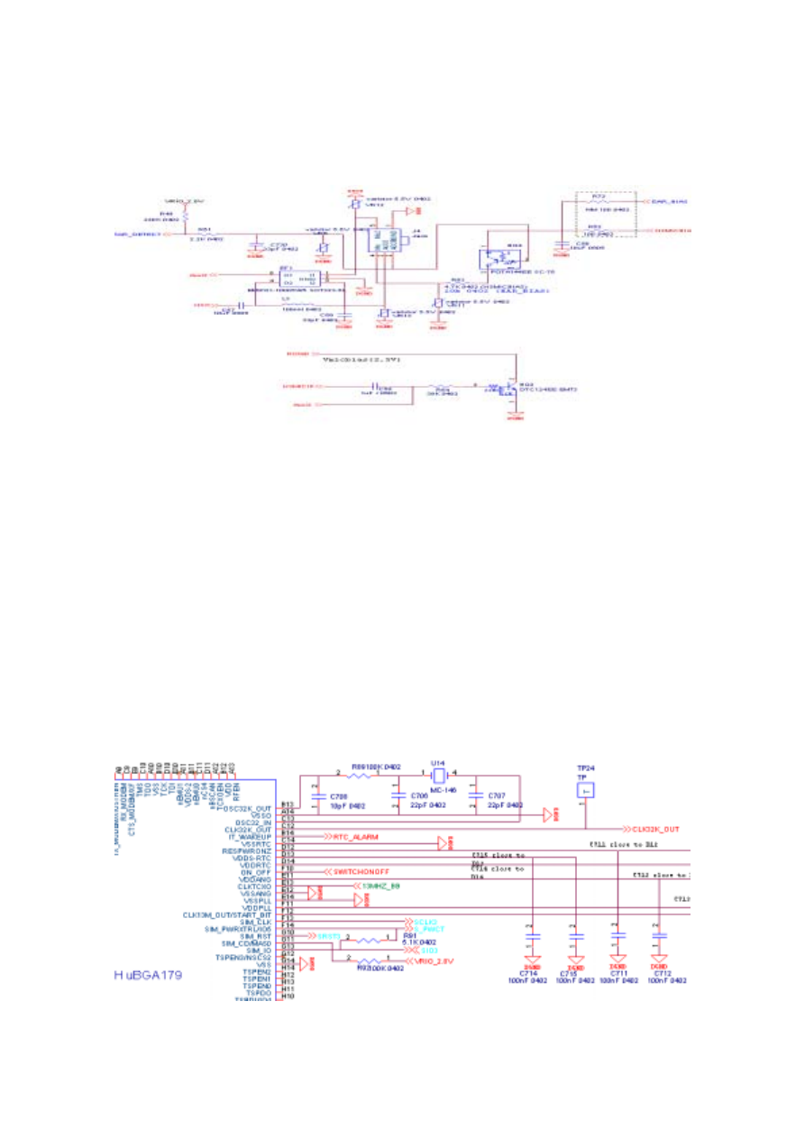
16. Can not record Time
•STEP 1.Check RTC battery whether powerful or failure
a. Change RTC battery.
•STEP 2.IF above-mentioned are all in normal condition then the problem could
be caused by M/B.
STEP 2.1.if TP24 <> 32.768K,then change a new U2.
STEP 2.2.if change a new U2 isn’t ok ,then change a new G2.
17. Can not Download
•STEP 1.Check Download Tool SET
11
a. Reset.
•STEP 2.Check use right Data cable or failure
a. Change Data cable.
•STEP 3.Check I/O Connector failure
a. Change I/O Connector.
•STEP 4.Check I/O Connector Pin3-Pin16 solder creak
a. I/O Connector Pin3-Pin16 re-soldering.
•STEP 5.IF above-mentioned are all in normal condition then the problem could
be caused by M/B.
STEP5.1.if TP4<>13M,then change a new 13M.
STEP5.2. if TP24=32.768k,then change a new flash.
STEP5.3.if TP24<>32.768k,then change G2.
STEP5.4.if TP24<>32.768k,then pull out G2.measure IOTA’s 5 modules
voltage whether in normal.
STEP5.5.if IOTA is ok, then change a new G2. Space final, you can download
software.
18 DSC no function
STEP 1..Check the connector of DSC and FPC
TP4(13M)
TP24(32K)
12
a. recombination
STEP 2.Check the DSC whether to louse
a. Change DSC
STEP 3 . check the DSC’s LDO whether have output voltage.
STEP3.1 If the COMS_EN <2.5V, then change the G2
STEP3.2 If the LDO (U13) has no voltage output, then change U13
C99
100nF 0402
DGND
RR9
100K 0402 nm
C97
2.2uF/6V
DGND
DGND
C700
10nF 0402
DGND
AVSSP
DD25V
L6
100nH 0402
AVDDP
2.5V FOR OV7645FB
D25V
D33V
DGND
VBAT
COMS_EN
L7
100nH 0402
C98
1uF/6V
U13
MIC2211-2.5/3.3BML
Vin
1
EN1
2
EN2
3
BYP
4
NC
7
NC
8
VOUT3.0
9
VOUT2.5
10
NC
5
GND
6
RR26
0 0603
S25V
L8
100nH 0402
RR26
1SS400 SC-79(W99685)
STEP 4. CLK13M_DSC have no 13MHz
a. Change the inverter U18.
DGND
RR14
10
C724
100pF
X7R
0402
10%
50V
RR15
1M
DGND
U18
TC7SHU04FU
SC70-5
NC
1
IN
2
GND
3
VCC
5
OUT
4
C723
100pF
0402
10%
50V
NPO
CLK13M_DSC
D33V
CLK13M_OUT
STEP5. check the U12.E10 have no 13MHz
a. change the U12
13
STEP6 move the CMOS sensor , then power on the handset and press
#02#.
If it can’t get the firmware version such as 1.08 . the U12’s data
bus or control bus could have some trouble
a. change the U12
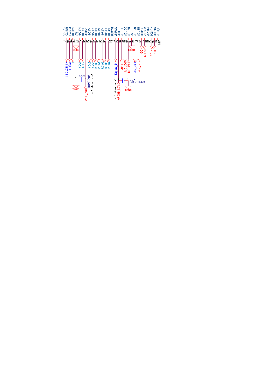
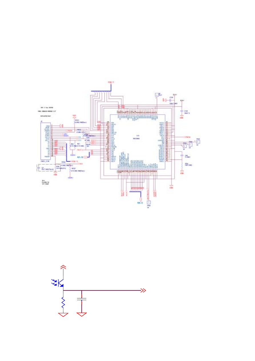
19. light sensor no function
step 1. check the VDDS-MIF-2.8V whether have 2.8V.
a. Check the BTB connector between M/B and MMI
step 2. check the LIGHTSENSER_EN whether have variably voltage
a. please change Q1 or R1.
DGND
LIGHTSENSER_EN
VDDS-MIF_2.8V
R1
10k
Q1
Photo-Transistor
DGND
C6
?nF 0402 NM
Step 3 check the LIGHTSENSER_EN have variably voltage
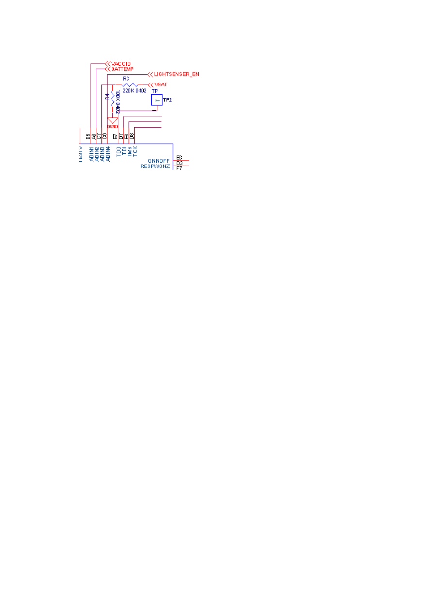
14
a. please change the IOTA.
15
△
Radio Frequency Descriptions
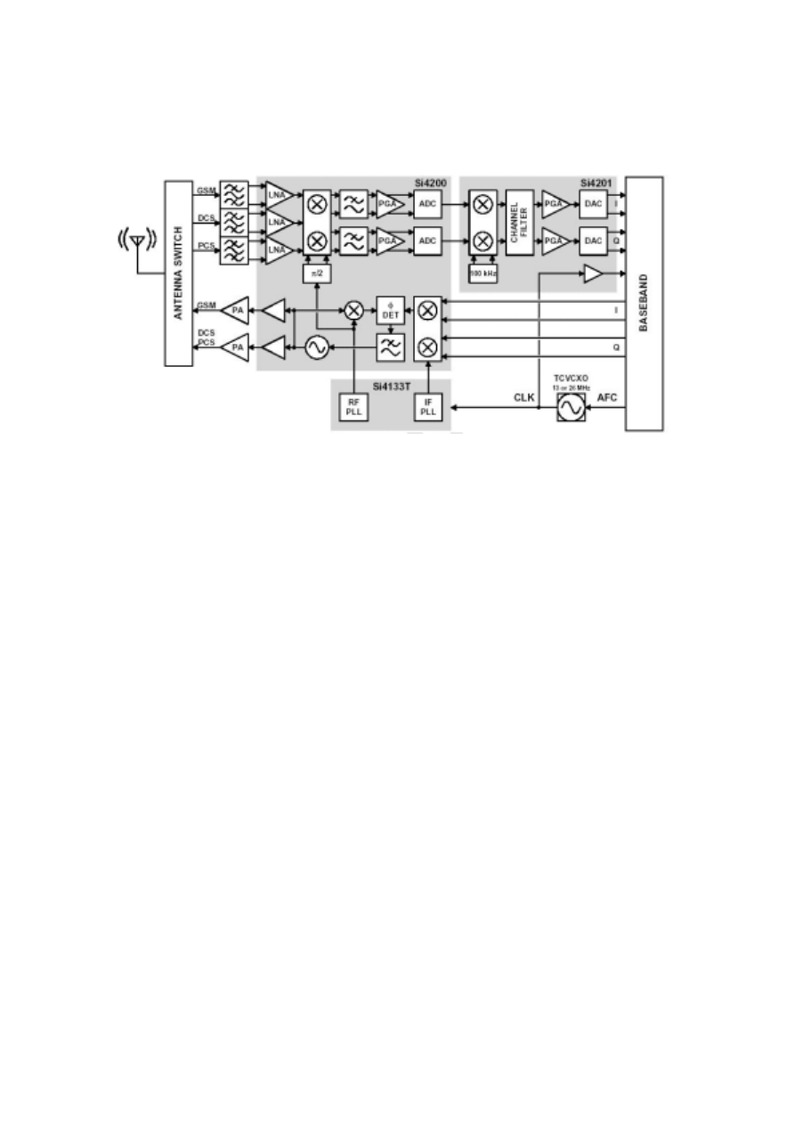
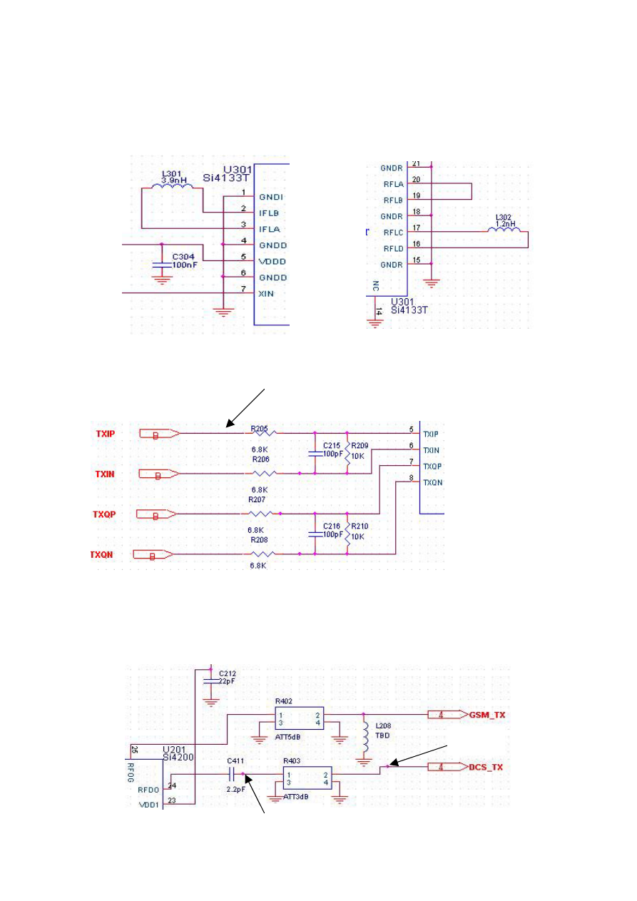
E365 RF Block Diagram :
The Aero transceiver consists of the Si4200 GSM transceiver, Si4201 universal
baseband interface, and Si4133T dual RF synthesizer. The highly integrated
solution eliminates the IF SAW filter, low noise amplifiers (LNAs) for three bands,
transmit and RF voltage controlled oscillator (VCO) modules, and more than 60
other discrete components found in conventional designs.
The receive section uses a digital low-IF architecture which avoids the difficulties
associated with directconversion while delivering lower solution cost and reduced
complexity. The universal baseband interface is compatible with any supplier’s
baseband subsystem.
The transmit section is a complete up conversion path from the baseband
subsystem to the power amplifier, and uses an offset phase locked loop (PLL) with
a fully integrated transmit VCO. The frequency synthesizer uses Silicon
Laboratories’ proven technology, which includes integrated RF and IF VCOs,
varactors and loopfilters.
16
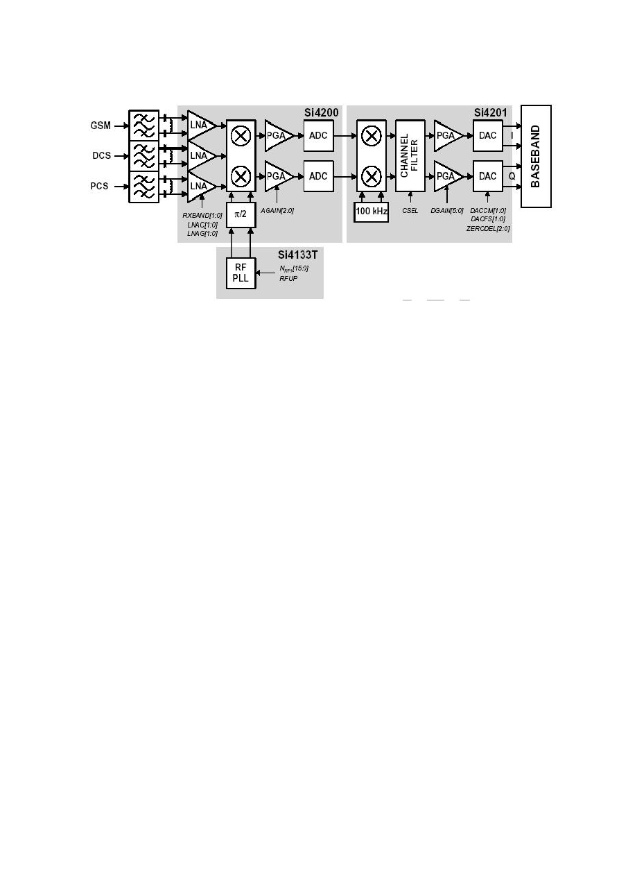
Receiver Block Diagram :
The Aero transceiver uses a low-IF receiver architecture that allows for the on-chip
integration of the channel selection filters. The Si4200 integrates three
differential-input LNAs. The LNA inputs are matched to the 200 Ohm balanced
output SAW filters through external LC matching networks.
A quadrature image-rejeject mixer downconverts the RF signal to a 100kHz
intermediate frequency (IF) with the RFLO from the Si4133T frequency
synthesizer. The mixer output is amplified with an analog programmable gain
amplifier (PGA). The quadrature IF signal is digitized with high resolution A/D
converters (ADCs).
The Si4201 downconverts the ADC output to baseband with a digital 100kHz
quadrature LO signal. Digital decimation and IIR filters perform channel selection
to remove blocking and reference interference signals. After channel selection, the
digital output is scaled with a digital PGA. DACs drive a differential analog signal
onto the RXIP, RXIN, RXQP and RXQN pins.
17
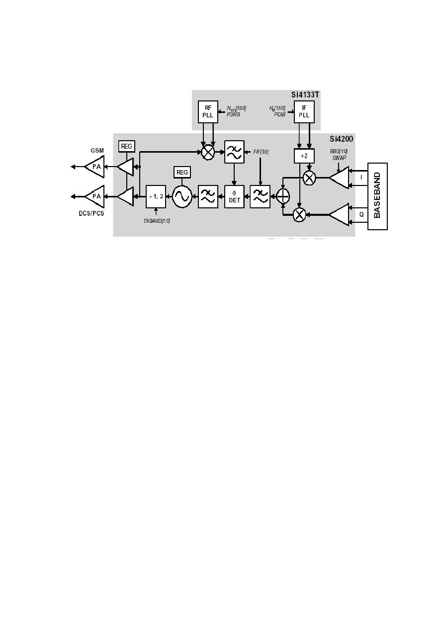
Transmitter Block Diagram :
The transmit (TX) section consists of an I/Q baseband upconverter, an offset
phase-locked loop (OPLL) and two 50 Ohm output buffers that can drive external
poweramplifiers (PA).
A quadrature mixer upconverts the differential in-phase (TXIP, TXIN) and
quadrature (TXQP, TXQN) signals with the IFLO to generate a SSB IF signal
which is filtered and used as the reference input to the OPLL. The Si4133
generates the IFLO frequency between 766MHz and 896 MHz. The IFLO is
divided by two to generate the quadrature LO signals for the quadrature
modulator, resulting in an IF between 383 and 448MHz.
The OPLL consists of a feedback mixer, a phase detector, a loop filter, and a fully
integrated TXVCO. The TXVCO is centered between the DCS1800 and PCS1900
bands, and its output is divided by two for the GSM 850 and E-GSM 900 bands.
The Si4133T generates the RFLO frequency between 1272 and 1483 MHz.
Low-pass filters before the OPLL phase detector reduce the harmonic content of
the quadrature modulator and feedback mixer outputs.
18
Frequency Plan of Aero
For Tx and Rx intermediate frequency plan
Tx intermediate frequency
Band
IF frequency (MHz) Channel
LO frequency (MHz)
399*2 975~1023
(890+0.2*(ARFCN-1024))+IF/2
399*2 0~24
(890+0.2*ARFCN)+IF/2
395*2 25~49
(890+0.2*ARFCN)+
IF/2
E-GSM
399*2 50~124
(890+0.2*
ARFCN)+
IF/2
DCS 383*2
512~885 (1710.2+0.2*(
ARFCN
-512))-IF/2
E-GSM : f
LO
=f
RF
+ f
IF
/2
DCS/PCS : f
LO
=f
RF
- f
IF
/2
Rx intermediate frequency 100kHz
Band
Channel
LO frequency (MHz)
975~1023 ((935+0.2*(ARFCN-1024))-0.1)*2
E-GSM
0~124 ((935+0.2*ARFCN)-0.1)*2
DCS 512~885
(1805.2+0.2*(ARFCN-512))-0.1
E-GSM: f
LO
/2 =f
RF
– 0.1 DCS / PCS: f
LO
=f
RF
– 0.1
Tx (Low, Mid, High channel)
Band
IF frequency(MHz)
LO frequency (MHz)
Channel
399*2 1279.2 975
399*2 1301.4 62
E-GSM
399*2 1313.8 124
383*2 1327.2 512
383*2 1364.6 699
DCS
383*2 1401.8 885
Rx (Low, Mid, High channel)
Band
LO frequency (MHz)
Channel
1850.2 975
1894.6 62
E-GSM
1919.4 124
1805.1 512
1842.5 699
DCS
1879.7 885
19
RX : GSM900
1. Set HP8960 or HP8922 : Operating mode : Test mode , Test function :
BCH+TCH
2. Ch 62 : 947.4MHz , cell power : -60dBm
3. Press
RX_900(62)
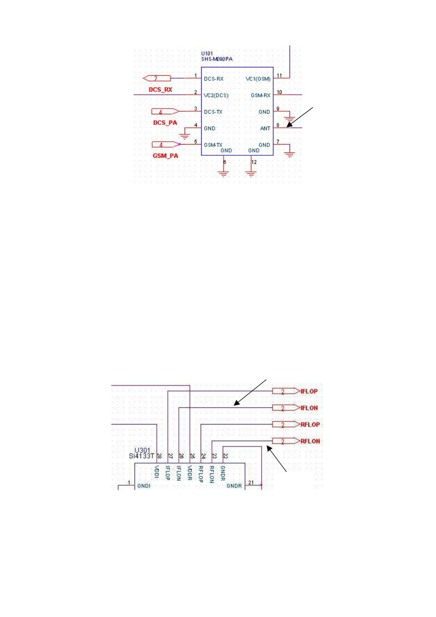
4. RX 900 signal 1 : Use probe to touch U101 pin 8 (freq = 947.4MHz)
5. RX 900 signal 2 : Use probe to touch U101 pin 10 (freq = 947.4MHz)
6. RX 900 signal 3 : Use probe to touch F101 pin 4/6 (freq = 947.4MHz)
Signal 2
Signal 1
Signal 3
20
7. RX 900 signal 4 : Use oscilloscope probe to touch RXQP, RXQN, RXIP,
RXIN from U203 pin 2~5 and you can find that ( For Example : The RXIP
signal )
Signal 4
21
RX : DCS1800
1. Set HP8960 or HP8922 : Operating mode : Test mode , Test function :
BCH+TCH
2. Ch 699 : 1842.6MHz , cell power : -60dBm
3. Press
RX_1800(699)
4. RX 1800 signal 1 : Use probe to touch U101 pin 8 (freq = 1842.6MHz)
5. RX 1800 signal 2 : Use probe to touch U101 pin 1 (freq = 1842.6MHz)
6. RX 1800 signal 3 : Use probe to touch F102 pin 4/6 (freq = 1842.6MHz)
Signal 1
Signal 2
Signal 3
22
TX : GSM900
1. Set HP8960 or HP8922 : Operating mode : Test mode , Test function :
BCH+TCH
2. Ch 62 : 902.4MHz , cell power : -60dBm , MS_TX_level : 5
3. Press
TX_900(62)
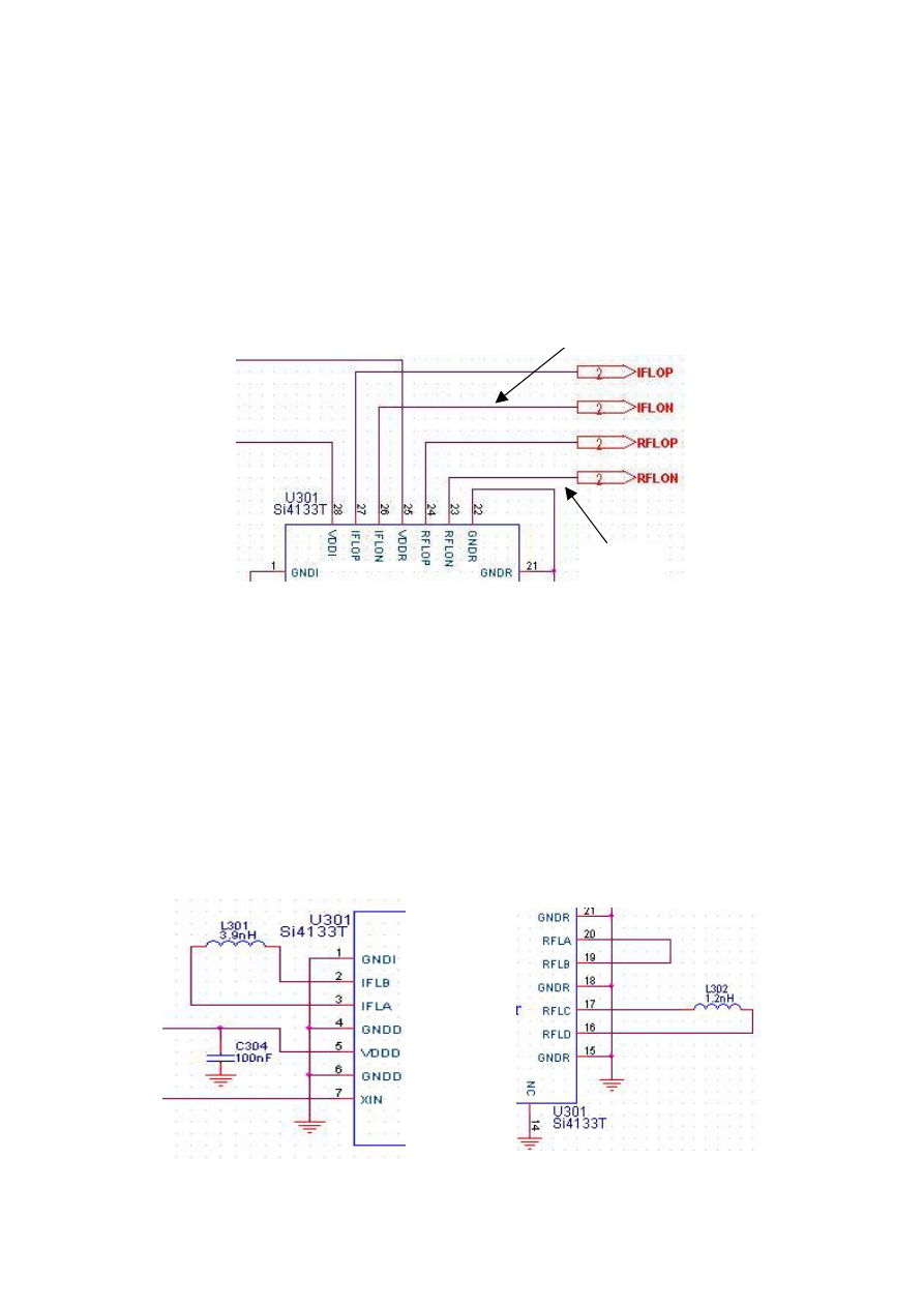
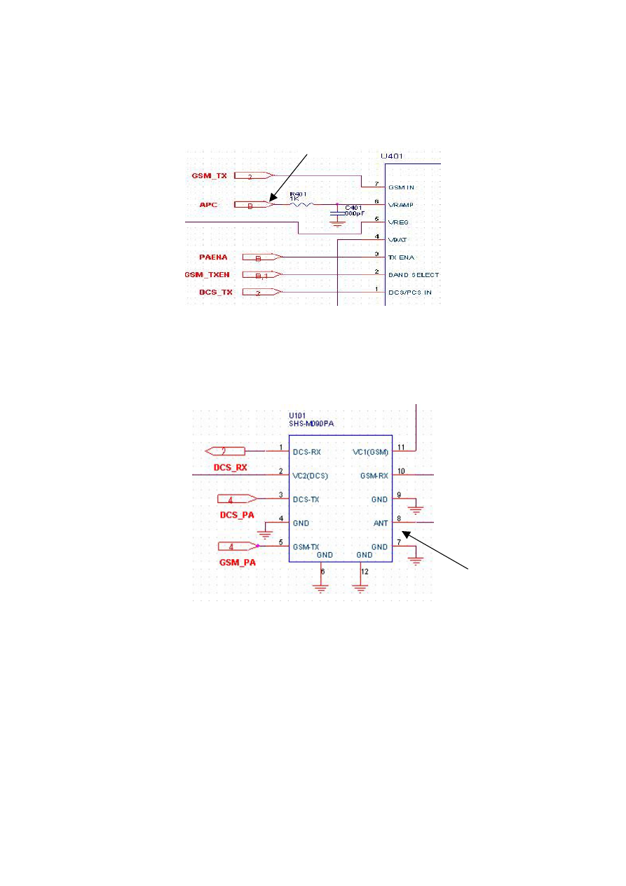
4. TX 900 signal 1 : Use probe to touch U301 pin 23/24 (freq = 1301.4MHz)
5. TX 900 signal 2 : Use probe to touch U301 pin 26/27 (freq = 798MHz)
( If signal 1 and 2 are OK, synthesizer and tranceiver are OK
If there are not then we have to check the inductor (L302 or L301) value
and solder)
Signal 2
Signal 1
23
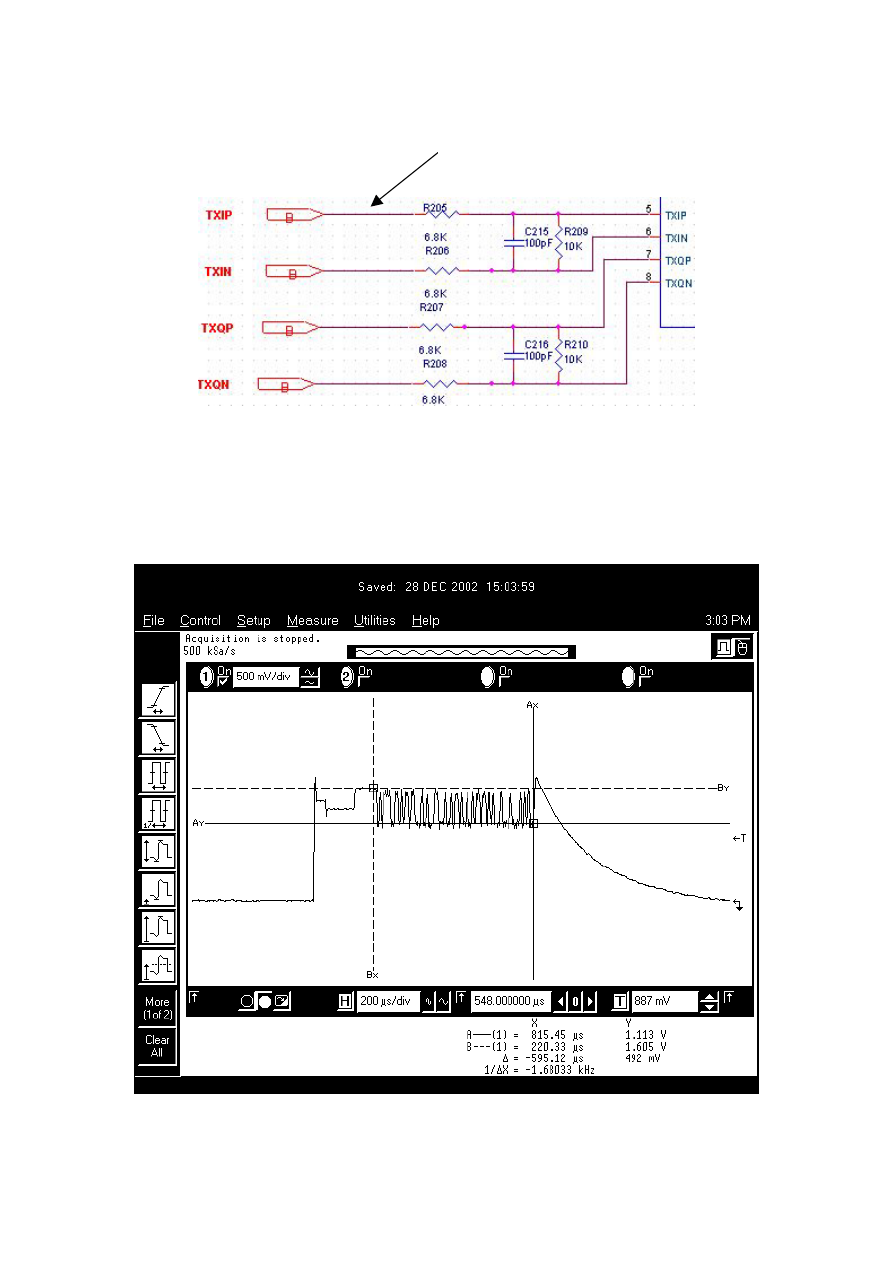
6. TX 900 signal 3 : Use oscilloscope probe to touch R205/6/7/8 pin 4/3 and you
can find that ( For Example : The TXIP signal )
Signal 3
24
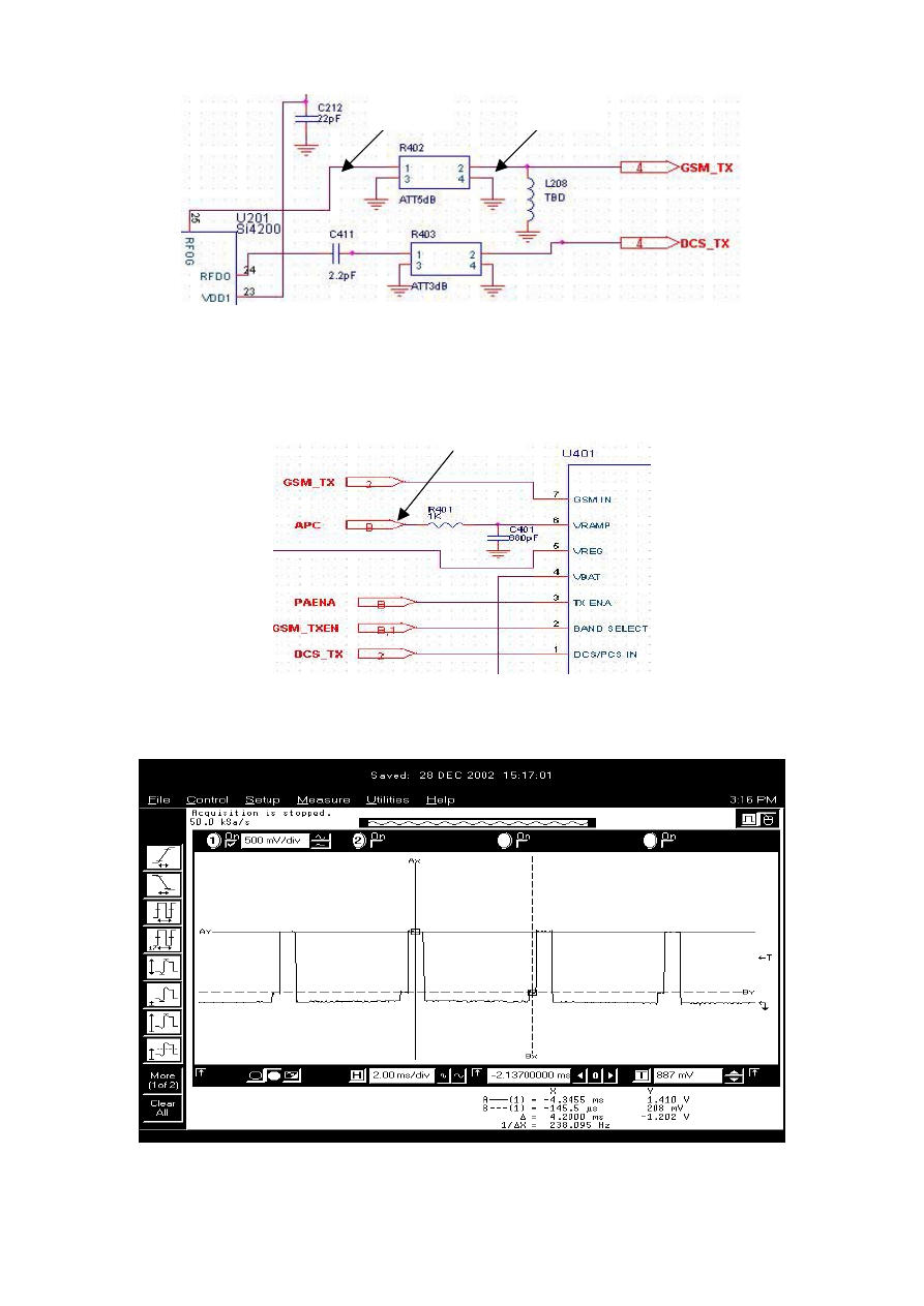
7. TX 900 signal 4 : Use probe to touch R402 pin 2 (frequency 902.4MHz)
8. TX 900 signal 5 : Use probe to touch R402 pin 1 (frequency 902.4MHz)
(If signal 4 and 5 are OK, TXVCO is OK.)
9. TX 900 signal 6 : Use oscilloscope probe to touch R401 and we can find that
Signal 4
Signal 5
Signal 6
25
10. TX 900 signal 7 : If 8960 or 8922 could show output power, PA is OK. If
8960 or 8922 show Freq_error, Peak_phase_error, RMS_phase_error are
inside the standard, Tx is OK.
TX : DCS1800
1. Set HP8960 or HP8922 : Operating mode : Test mode , Test function :
BCH+TCH
2. Ch 699 : 1747.6MHz , cell power : -60dBm , MS_TX_level : 0
3. Press
TX_1800(699)
4. TX 1800 signal 1 : Use probe to touch U301 pin 23/24 (freq = 1364.6MHz)
5. TX 1800 signal 2 : Use probe to touch U301 pin 26/27 (freq = 766MHz)
( If signal 1 and 2 are OK, synthesizer and tranceiver are OK
Signal 2
Signal 1
Signal 7
26
If there are not then we have to check the inductor (L302 or L301) value and
solder)
6. TX 1800 signal 3 : Use oscilloscope probe to touch R205/6/7/8 pin 4 (3) and
the result is similar to the GSM TXIQ.
Signal 4
Signal 5
Signal 3
27
7. TX 1800 signal 4 : Use probe to touch R403 pin 2 (frequency 1747.6MHz)
8. TX 1800 signal 5 : Use probe to touch R403 pin 1 (frequency 1747.6MHz)
(If signal 4 and 5 are OK, TXVCO is OK.)
9. TX 1800 signal 6 : Use oscilloscope probe to touch R401 and the diagram is
similar to GSM APC.
10. TX 1800 signal 7 : If 8960 or 8922 could show output power, PA is OK. If
8960 or 8922 show Freq_error, Peak_phase_error, RMS_phase_error are
inside the standard, Tx is OK.
Signal 6
Signal 7
Wyszukiwarka
Podobne podstrony:
CD CiDeCo E365 A4 C L3 1[1] 0 030610085958
PL PaLi E365 A4 C L3 1[1] 0 030605160430
BD BlDi E365 A3 C L3 1[1] 2 030611100711
BL E365 A4 BW L3 V1[1] 1
TS V180 A4 L3 V1[1] 2
TS Triplets Refresh A4 C L3 V1[1] 1
SiDe C115 A4 C L3 1[1] 0 040707025807
CD P7689 A4 C L3 V1 0
pl v661 a4 c l3 v10
PL V3 05 A4 C L3 1 0
Parts List V200 V220 A4 C L3 8486890P01
PL V180 8486962P01 P3 A4 C L3 V1[1] 1
Circuit Description W510 A4 C L3 v1 Description
PspJEAP DCSST85 A4 C L3 Vxx
BL T193 A4 L3 BW 84D86506P03 RevB V2001 07 25
BDSD TriplestR A4 C L3 V1[1] 0
SchRF T191 1900 C A4 L3 V1 0
Sch V175 A4 C L3 1 0
więcej podobnych podstron