Multi-Winding Transformer Based Diode-
Clamped Multi-Level Inverter
Ehsan Esfandiari
Electronic&Electrical Engineering Dept.
University Putra Malaysia/Islamic Azad University,
Majlesi Branch
Serdang, Malaysia/Esfahan, Iran
Ehsan.esf@gmail.com
Norman Bin Mariun
Electronic&Electrical Engineering Dept.
University Putra Malaysia
Serdang, Malaysia
norman@eng.upm.edu.my
Abstract—In this paper, a new configuration for diode-
clamped multilevel inverter based on multi-winding
transformer is proposed, described and simulated. The most
important difference between this proposed DC-AC-AC
structure and basic structure is that in the proposed
structure, back-to-back connected outputs of a multi-
winding transformer are superseded the capacitors in basic
structure. Simulation a 7 levels of proposed configuration
shows 10% THD.
key words: multi-winding, multi-level inverter, Diode-Clamped
I. I
NTRODUCTION
Recently there has been much interest in multilevel
inverters. Multilevel inverters synthesize a desired
voltage close to sinusoidal voltage using separated or
back-to-back connected voltage sources [1-10].
From the perspective of the control method, inverters
can be classified into two major groups:
1- Line-Frequency controlled multilevel inverters.
2- PWM-controlled multilevel inverters.
In first case, switches are controlled by low frequency
signals and generate a staircase output. The more the
number of the levels, the lower the THD and
⁄ .across the switches. In the second case, switches
are controlled by a high frequency PWM signals.
The Diode-Clamped multilevel inverter was
introduced by some scientists in last decade, [2, 11-13].
The basic structure of Diode-Clamped is based on N
series-connected capacitors as DC sources that load is
clamped to them to reach to desired output voltage. Also,
[14] describes the improved Diode-Clamped inverter.
Unbalancing in capacitor`s voltage is a problem in
Diode-Clamped [7]. In this paper a new configuration
based on multi-winding transformer as voltage sources
and the configuration discussed in [14] is proposed and a
7 levels inverter is simulated.
II. B
ASIC STRUCTURE OF PROPOSED INVERTER
This inverter, as shown in Fig. 1, is a low frequency
DC-AC-AC converter. It consists of an H-Bridge Block
and a switch array similar to Diode-Clamped structure.
H-Bridge Block converts the DC voltage of the source
to a low frequency square wave AC voltage. This voltage
is applied to the primary of a multiwinding transformer.
Transformer converters this square wave input to a
multiple synchronous low frequency outputs with
desirable amplitude. By choosing an appropriate
switching strategy, it is possible to add these voltages to
synthesize a desired sinusoidal output.
A. Normal operation of circuit in positive cycle
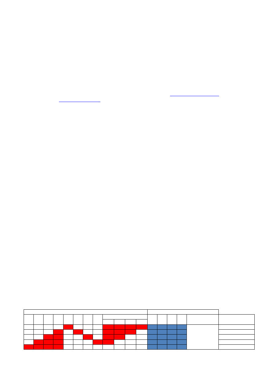
Table 1 shows the switching strategy for positive cycle
for proposed inverter. For all of instances in positive
cycle to and
to
from Block B are off also,
to are on (standby for freewheeling path).
If and from Block A are turned on, output equals
. In this stage,
to
are kept on to provide probable
freewheeling path. If , and are turned on output
equals
. In this stage,
to
are kept on to
provide probable freewheeling path.
If
,
,
and
are turned on, output equals
. In this stage,
is kept on to provide
freewheeling path. Fig. 1 shows this condition.
To reach to maximum in positive cycle, to are
turned on. In this case,
to
from Block A and to
from Block B provide freewheeling path.
At last, to reach to output equal to zero, and
to
from Block A are turned on. Thus, forward current
path includes
to
from Block B and and
T
ABLE
1
S
WITCHING PATTERN FOR POSITIVE CYCLE
Switches in Block A
Switches in Block B
S1 S2 S3 S4 S5 S6 S7 S8
Freewheeling path
S1 S2 S3 S4
S5 to S8 and
S1’ to S4’
output
S1’ S2’ S3’ S4’
0 0 0 0 1 0 0 0 1
1
1
1
1
1
1
1
0
0
0 0 0 1 0 1 0 0 1
1
1 0 1
1
1
1 +V1
0 0 1
1 0 0 1 0 1
1 0 0 1
1
1
1 +V1+V2
0
1
1
1 0 0 0 1
1 0 0 0 1
1
1
1 +V1+V2+V3
1
1
1
1 0 0 0 0 0 0 0 0 1
1
1
1 +V1+V2+V3+V4
2010 IEEE Symposium on Industrial Electronics and Applications (ISIEA 2010), October 3-5, 2010, Penang, Malaysia
978-1-4244-7647-3/10/$26.00 ©2010 IEEE
155
to
from block A.
The important point is that in the positive cycle, to
from Block B must be kept off, unless, short circuit is
occurred. Even in the dead time of H-Bridge (from
positive to zero), because there may be some stored
energy in secondary, turning on from Block B will
causes a short circuit.
B. Normal operation of circuit in negative cycle
Table 2 shows the switching strategy for negative
cycle. For all of instances in negative cycle to and
to
from Block A are off and to
are on
(standby for freewheeling path).
If
and
(from Block B) are turned on output
equals
. In this stage, to
are kept on to provide
probable freewheeling path.
If
,
and
from Block B are turned on output
equals
–
. In this stage, to
are kept on to
provide probable freewheeling path.
If
,
,
and
are turned on output equals
–
. In this stage, is kept on to provide
freewheeling path.
T
ABLE
2
S
WITCHING PATTERN FOR NEGATIVE CYCLE
Switches in block B
Switches in block A
S1 S2 S3 S4 S5 S6 S7 S8
Freewheeling path
S1 S2 S3 S4
S5 to S8 and
S1’ to S4’
output
S1’ S2’ S3’ S4’
0 0 0 0 1 0 0 0 1
1
1
1
1
1
1
1
0
0
0 0 0 1 0 1 0 0 1
1
1 0 1
1
1
1 -V4
0 0 1
1 0 0 1 0 1
1 0 0 1
1
1
1 -V4-V3
0
1
1
1 0 0 0 1
1 0 0 0 1
1
1
1 -V4-V3-V2
1
1
1
1 0 0 0 0 0 0 0 0 1
1
1
1 -V4-V3-V2-V1
Load
-Vout+
Fig. 1 Forward and freewheeling current path for inverter when output voltage equals +V1+V2+V3
Forward current path
Freewheeling current path
+
-
+
-
+
-
156
To reach to minimum in the negative cycle, to are
turned on. In this case,
to
from Block B and to
from Block A provide freewheeling path.
At last, to reach to the output equals to zero, and
to
are turned on. So forward current path includes
to
from Block B and and
to
from Block
A.
The important point is that in the negative cycle, to
from Block A must be kept off, unless, short circuit is
occurred. Even in dead time of H-Bridge (from negative
to zero), because there may be some stored energy in
secondary, turning on from Block A will causes a
short circuit.
III. S
IMULATION
OrCAD16.2 was used to simulate a 7 level of proposed
inverter. The auto-convergence ability of this software
provides condition to simulate high current and voltages
beside low current and voltages of controlling modules
1
.
For simulating the multi-winding transformer the
ladder model proposed in [15] was applied. To reach to
1
Please note that our try to simulate the proposed
structure using OrCAD16 failed because of convergence
problem.
Fig. 2 A) Voltage across a 10Ω resistive load B) Current passing through C) THD of voltage D) Output current for a pure inductive
load
Time
0s
2ms
4ms
6ms
8ms
10ms
12ms
14ms
16ms
18ms
20ms
-I(Rload)
-10A
0A
10A
Time
0s
2ms
4ms
6ms
8ms
10ms
12ms
14ms
16ms
18ms
20ms
V(Rload:2,SB4):D)
-100V
0V
100V
Frequency
V(Rload:2,SB4):D)
0Hz
0.2KHz
0.4KHz
0.6KHz
0.8KHz
1.0KHz
1.2KHz
1.4KHz
0V
40V
80V
Time
0s
2ms
4ms
6ms
8ms
10ms
12ms
14ms
16ms
18ms
20ms
- I(L1:1)
-40A
0A
40A
A
B
C
D
157
near sinusoidal output, firing angles for Mosfets was
calculated from this equation[16] :
.
(1)
Where, N is the number of sources.
Fig. 2 illustrates the simulation results for a 7 levels of
proposed inverter with Mosfet switches. Fig. 2.A and Fig.
2.B are the voltage and current through a 10Ω resistive
load. Fig. 2.C is the FFT of the voltage across the 10Ω
load. The THD became more than 10%. Fig. 2.D shows
the current through a pure inductive load. This proves the
ability of propose inverter to feed inductive loads. The
schematic of switches is shown in
Fig. 3
.
IV. C
ONCLUSION
A new configuration for diode-clamped multilevel
inverter was proposed and simulated. In the proposed
Diode-Clamped structure, capacitors were replaced by a
multi-winding transformer to shape a DC-AC-AC
converter. The structure has very simple switching
strategy. The simulation results for a stepped output show
ability of this inverter to feed resistive and inductive
loads. Simulating a seven levels inverter shows 10%
THD for a 10Ω resistive load.
References
[1]
L. M. Tolbert, F. Z. Peng, and T. G. Habetler, "Multilevel
Converters for Large Electric Drives," IEEE
TRANSACTIONS ON INDUSTRY APPLICATIONS, vol. 35,
1999.
[2]
M. Carpita, S. M. Tenconi, and M. Fracchia, "A novel
multilevel structure for voltage source inverter," 1992, pp.
90-90.
[3]
K. Corzine and Y. Familiant, "A new cascaded multilevel H-
bridge drive," IEEE Transactions on power electronics, vol.
17, pp. 125-131, 2002.
[4]
S. Daher, J. Schmid, and F. L. M. Antunes, "Design and
Implementation of an Asymmetrical Multilevel Inverter for
Renewable Energy Systems," 2005, pp. 199-204.
[5]
S. Daher, J. Schmid, and F. L. M. Antunes, "Multilevel
Inverter Topologies for Stand-Alone PV Systems," IEEE
Transactions on Industrial Electronics, vol. 55, pp. 2703-
2712, 2008.
[6]
P. W. Hammond, "A new approach to enhance power quality
for medium voltage AC drives," IEEE Transactions on
Industry Applications, vol. 33, pp. 202-208, 1997.
[7]
J. S. Lai and F. Z. Peng, "Multilevel converters-a new breed
of power converters," IEEE Transactions on Industry
Applications, vol. 32, pp. 509-517, 1996.
[8]
T. A. Meynard and H. Foch, "Multi-level choppers for high
voltage applications," EPE journal, vol. 2, pp. 45-50, March
1992.
[9]
C. Newton and M. Sumner, "Multilevel converters: A real
solution to medium high voltage drives?," Institiute of
Electronic Engineering Power Engineering pp. 21–26, Feb.
1998 1998.
[10]
E. Esfandiari, N. Mariun, M. H. Marhaban, and A. Zakaria,
"Switch-ladder: reliable and efficient multilevel inverter,"
Electronics Letters, vol. 46, p. 646, April 2010.
[11]
J. M. Andrejak and M. Lescure, "High voltage converters
promising technological developments," in Proc. Rec. EPE
Conf., 1987, pp. 1.159-1.162.
[12]
A. Nabae, I. Takahashi, and H. Akagi, "A new neutral-point-
clamped PWM inverter," IEEE Transactions on Industry
Applications, pp. 518-523, 1981.
[13]
N. S. Choi, J. G. Cho, and G. H. Cho, "A general circuit
topology of multilevel inverter," in Power Electronics
Specialists Conference, 1991. PESC '91 Record., 22nd
Annual IEEE, 1991, pp. 96-103, 24-27
[14]
X. Yuan and I. Barbi, "Fundamentals of a new diode
clamping multilevel inverter," IEEE Transactions on Power
Electronics, vol. 15, pp. 711-718, 2000.
[15]
J. Wang, A. F. Witulski, J. L. Vollin, T. K. Phelps, and G. I.
Cardwell, "Derivation, calculation and measurement of
parameters for amulti-winding transformer electrical model,"
1999.
[16]
R. W. Menzies and Y. Zhuang, "Advanced static
compensation using a multilevel GTO thyristor inverter,"
IEEE Transactions on Power Delivery, vol. 10, pp. 732-738,
1995.
G
Ds
D1N3495
D4
Rs
100
Cs
47n
V1
15
R28
.1
S
D
RGP
1k
U
1
PS256
1
1
2
3
4
R3
200
0
RG
10
M1
IRF3808
Fig. 3. Schematic of switches that was used for simulation
158
Wyszukiwarka
Podobne podstrony:
Novel Multi level Inverter Topology Based on Multi Winding Multi Trapped Transformers for Improved W
Isolated Multi level Inverter Using 3 Phase Transformers
Isolated Multi level Inverter Using 3 Phase Transformers
Design and construction of three phase transformer for a 1 kW multi level converter
A Trust System Based on Multi Level Virus Detection
03 Multi Level Arrays
Implementation of a Mu;ti level Inverter Based on Selective Harmonic Elimination and Zig Zag Connect
2810 Transfer case, checking & correcting fluid level
NDT 52517 a novel 5 category multi modal t1 and t2wi mri based strati 031914
NDT 52517 a novel 5 category multi modal t1 and t2wi mri based strati 031914
multi demultiplekser
LG MULTI V
więcej podobnych podstron