PIONEER ELECTRONIC CORPORATION
4-1, Meguro 1-Chome, Meguro-ku, Tokyo 153-8654, Japan
PIONEER ELECTRONICS SERVICE INC.
P.O.Box 1760, Long Beach, CA 90801-1760 U.S.A.
PIONEER ELECTRONIC [EUROPE] N.V.
Haven 1087 Keetberglaan 1, 9120 Melsele, Belgium
PIONEER ELECTRONICS ASIACENTRE PTE.LTD.
253 Alexandra Road, #04-01, Singapore 159936
C
PIONEER ELECTRONIC CORPORATION 1998
K-ZZD. DEC. 1998 Printed in Japan
ORDER NO.
CRT2313
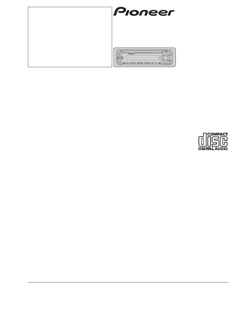
HIGH POWER CD PLAYER WITH FM/AM TUNER
DEH-1000
X
1
N/UC
Service
Manual
CONTENTS
1. SAFETY INFORMATION ............................................2
2. EXPLODED VIEWS AND PARTS LIST .......................2
3. SCHEMATIC DIAGRAM ...........................................12
4. PCB CONNECTION DIAGRAM ................................28
5. ELECTRICAL PARTS LIST ........................................38
6. ADJUSTMENT..........................................................44
7. GENERAL INFORMATION .......................................48
7.1 PARTS .................................................................48
7.1.1 IC................................................................48
7.1.2 DISPLAY ....................................................55
7.2 DIAGNOSIS ........................................................56
7.2.1 DISASSEMBLY .........................................56
7.2.2 TEST MODE ..............................................57
7.3 BLOCK DIAGRAM ..............................................61
8. OPERATIONS AND SPECIFICATIONS.....................62
- See the separate manual CX-916(CRT2300) for the CD mechanism description, disassembly and circuit
description.
- The CD mechanism employed in this model is one of S8 series.
DEH-10
X
1
N/UC
DEH-1050
X
1
N/ES
DEH-1000/X1N/UC
2
DEH-1000,10,1050
- CD Player Service Precautions
1. For pickup unit(CXX1285) handling, please refer
to"Disassembly"(CX-916 Service Manual CRT2300).
During replacement, handling precautions shall be
taken to prevent an electrostatic discharge(protection
by a short pin).
2. During disassembly, be sure to turn the power off
since an internal IC might be destroyed when a con-
nector is plugged or unplugged.
3. Please checking the grating after changing the ser-
vice pickup unit(see page 46).
CAUTION
This service manual is intended for qualified service technicians; it is not meant for the casual do-it-yourselfer.
Qualified technicians have the necessary test equipment and tools, and have been trained to properly and safely repair
complex products such as those covered by this manual.
Improperly performed repairs can adversely affect the safety and reliability of the product and may void the warranty.
If you are not qualified to perform the repair of this product properly and safely; you should not risk trying to do so
and refer the repair to a qualified service technician.
WARNING
This product contains lead in solder and certain electrical parts contain chemicals which are known to the state of
California to cause cancer, birth defects or other reproductive harm.
Health & Safety Code Section 25249.6 - Proposition 65
1. SAFETY INFORMATION
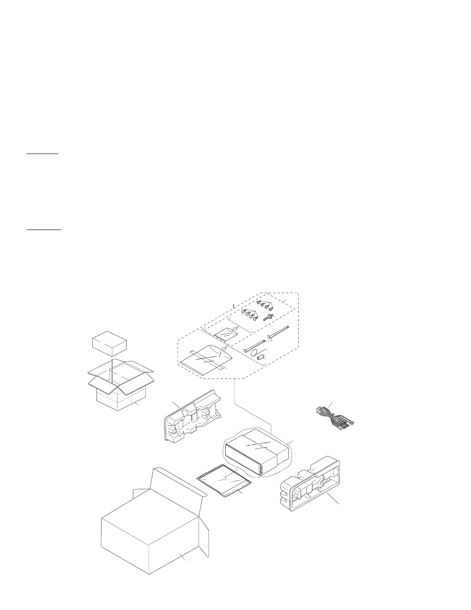
2. EXPLODED VIEWS AND PARTS LIST
2.1 PACKING
20
15
12
16
17
4
7
11
3
10
9
8
6
5
2
14
1
3
DEH-1000,10,1050
- Owner’s Manual
Model
Part No.
Language
DEH-1000/X1N/UC, DEH-10/X1N/UC
CRD2858
English, French, Spanish
DEH-1050/X1N/ES
CRD2860
English, Spanish, Portuguese
CRD2861
Arabic, Chinese
- Installation Manual
Model
Part No.
Language
DEH-1000/X1N/UC, DEH-10/X1N/UC
CRD2859
English, French, Spanish
DEH-1050/X1N/ES
CRD2862
English, Spanish, Portuguese, Arabic, Chinese
1 Cord Assy
CDE5874
*
2 Accessory Assy
CEA2395
3 Spring
CBH1650
4 Screw Assy
CEA2396
5 Screw
CBA1002
*
6 Polyethylene Bag
CEG-127
7 Screw
CRZ50P090FMC
8 Screw
TRZ50P080FMC
*
9 Polyethylene Bag
CEG-158
10 Handle
CNC5395
11 Bush
CNV3930
12 Polyethylene Bag
See Contrast table(2)
13 •••••
14 Carton
See Contrast table(2)
15 Contain Box
See Contrast table(2)
16 Protector
CHP2101
17 Protector
CHP2102
18 •••••
19 •••••
20-1 Owner’s Manual
See Contrast table(2)
20-2 Owner’s Manual
See Contrast table(2)
20-3 Installation Manual
See Contrast table(2)
20-4 Polyethylene Bag
CEG1116
* 20-5 Card
See Contrast table(2)
Mark No. Description
Part No.
Mark No. Description
Part No.
(1) PACKING SECTION PARTS LIST
NOTE:
- Parts marked by “*” and | can not be supplied.
- Screws adjacent to
∇
mark on the product are used for disassembly.
Part No.
Mark No. Symbol and Description DEH-1000/X1N/UC
DEH-10/X1N/UC
DEH-1050/X1N/ES
12 Polyethylene Bag
CEG1173
CEG1173
CEG-162
14 Carton
CHG3664
CHG3663
CHG3665
15 Contain Box
CHL3664
CHL3663
CHL3665
20-1 Owner’s Manual
CRD2858
CRD2858
CRD2860
20-2 Owner’s Manual
Not used
Not used
CRD2861
20-3 Installation Manual
CRD2859
CRD2859
CRD2862
* 20-5 Card
ARY1048
ARY1048
Not used
(2) CONTRAST TABLE
DEH-1000/X1N/UC, DEH-10/X1N/UC and DEH-1050/X1N/ES are constructed the same except for the fol-
lowing:

4
DEH-1000,10,1050
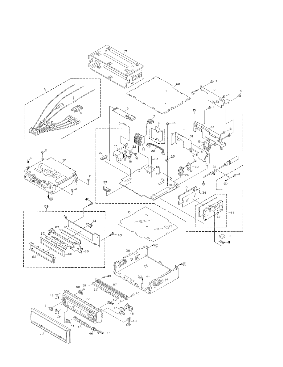
2.2 EXTERIOR
- DEH-1000/X1N/UC

5
DEH-1000,10,1050
1 Screw
BMZ26P120FMC
2 Screw
BSZ26P060FMC
3 Screw
BSZ30P060FMC
4 Screw
BSZ30P120FMC
5 Cable
CDE6018
6 Cord Assy
CDE5874
7 Fuse(10A)
CEK1136
8 Resistor
RS1/2PMF102J
9 Cap
CNS1472
10 Cover
CNC8367
11 Earth Plate
CNC8368
12 Spacer
CNM4913
13 Insulator
CNM6006
14 Insulator
CNM6224
|
15 Tuner Amp Unit
CWM6092
16 Screw
ASZ26P080FMC
17 Screw
BPZ26P080FMC
18 Screw
BSZ26P160FMC
19 IC(IC551)
PAL005A
20 Connector(CN551)
CDE5996
21 Antenna Cable(CN502)
CDH1254
22 Transistor(Q981,991)
2SD2396
23 Clamper
CEF1006
24 Pin Jack(CN431)
CKB1028
25 Terminal(CN501)
CKF1059
26 Connector(CN951)
CKM1299
*
27 Connector(CN681)
CKS2227
28 •••••
29 Connector(CN651)
CKS3581
30 Holder
CNC7533
31 Holder
CNC8130
32 Holder
CNC8041
33 Holder
CNC8043
34 Insulator
CNM5967
35 Heat Sink
CNR1506
36 FM/AM Tuner Unit
CWE1501
37 Holder
CNC7532
38 Chassis Unit
CXB3167
39 Screw
BPZ20P060FMC
40 Screw
BPZ20P080FMC
41 Button(+)
CAC5834
42 Button(-)
CAC5837
43 Button(SOURCE)
CAC5983
44 Button(BAND)
CAC5984
45 Button(1-6)
CAC5840
46 Button(PGM,CL)
CAC5841
47 Button(UP,DOWN)
CAC5846
48 Button(<>)
CAC5849
49 Button(F,A)
CAC5852
50 Button(EJECT)
CAC5853
51 Button(EQ)
CAC6132
52 Cover
CNM4704
53 •••••
54 •••••
55 •••••
56 •••••
57 Holder
CNV5574
58 Housing
CNV5575
59 Keyboard Unit
CWM6098
60 LCD(LCD1801)
CAW1500
61 Connector(CN1801)
CKS3580
62 Holder
CNC8036
63 Sheet
CNM6026
64 •••••
65 Screw
ISS26P055FUC
66 Lighting Conductor
CNV5570
67 Connector
CNV5571
68 Grille Unit
CXB3504
69 Case Unit
CXB4033
70 CD Mechanism Module
CXK5200
71 Holder
CNC6798
72 Panel
CNS5132
- EXTERIOR SECTION PARTS LIST
Mark No. Description
Part No.
Mark No. Description
Part No.
6
DEH-1000,10,1050
- DEH-10/X1N/UC

7
DEH-1000,10,1050
1 Screw
BMZ26P120FMC
2 Screw
BSZ26P060FMC
3 Screw
BSZ30P060FMC
4 Screw
BSZ30P120FMC
5 Cable
CDE6018
6 Cord Assy
CDE5874
7 Fuse(10A)
CEK1136
8 Resistor
RS1/2PMF102J
9 Cap
CNS1472
10 Cover
CNC8367
11 Earth Plate
CNC8368
12 Spacer
CNM4913
13 Insulator
CNM6006
14 Insulator
CNM6224
|
15 Tuner Amp Unit
CWM6092
16 Screw
ASZ26P080FMC
17 Screw
BPZ26P080FMC
18 Screw
BSZ26P160FMC
19 IC(IC551)
PAL005A
20 Connector(CN551)
CDE5996
21 Antenna Cable(CN502)
CDH1254
22 Transistor(Q981,991)
2SD2396
23 Clamper
CEF1006
24 Pin Jack(CN431)
CKB1028
25 Terminal(CN501)
CKF1059
26 Connector(CN951)
CKM1299
*
27 Connector(CN681)
CKS2227
28 •••••
29 Connector(CN651)
CKS3581
30 Holder
CNC7533
31 Holder
CNC8130
32 Holder
CNC8041
33 Holder
CNC8043
34 Insulator
CNM5967
35 Heat Sink
CNR1506
36 FM/AM Tuner Unit
CWE1501
37 Holder
CNC7532
38 Chassis Unit
CXB3167
39 Screw
BPZ20P060FMC
40 Screw
BPZ20P080FMC
41 Button(+)
CAC5834
42 Button(-)
CAC5837
43 Button(SOURCE)
CAC5983
44 Button(BAND)
CAC5984
45 Button(1-6)
CAC5840
46 Button(PGM,CL)
CAC5841
47 Button(UP,DOWN)
CAC5846
48 Button(<>)
CAC5849
49 Button(F,A)
CAC5852
50 Button(EJECT)
CAC5853
51 Button(EQ)
CAC6132
52 Cover
CNM4704
53 •••••
54 •••••
55 •••••
56 •••••
57 Holder
CNV5574
58 Housing
CNV5575
59 Keyboard Unit
CWM6095
60 LCD(LCD1801)
CAW1500
61 Connector(CN1801)
CKS3580
62 Holder
CNC8036
63 Sheet
CNM6026
64 •••••
65 Screw
ISS26P055FUC
66 Lighting Conductor
CNV5570
67 Connector
CNV5571
68 Grille Unit
CXB3503
69 Case Unit
CXB4033
70 CD Mechanism Module
CXK5200
71 Holder
CNC6798
72 Panel
CNS5132
- EXTERIOR SECTION PARTS LIST
Mark No. Description
Part No.
Mark No. Description
Part No.

8
DEH-1000,10,1050
- DEH-1050/X1N/ES

9
DEH-1000,10,1050
1 Screw
BMZ26P120FMC
2 Screw
BSZ26P060FMC
3 Screw
BSZ30P060FMC
4 Screw
BSZ30P120FMC
5 Cable
CDE6018
6 Cord Assy
CDE5874
7 Fuse(10A)
CEK1136
8 Resistor
RS1/2PMF102J
9 Cap
CNS1472
10 Cover
CNC8367
11 Earth Plate
CNC8368
12 Spacer
CNM4913
13 Insulator
CNM6006
14 Insulator
CNM6224
|
15 Tuner Amp Unit
CWM6093
16 Screw
ASZ26P080FMC
17 Screw
BPZ26P080FMC
18 Screw
BSZ26P160FMC
19 IC(IC551)
PAL005A
20 Connector(CN551)
CDE5996
21 Antenna Cable(CN502)
CDH1254
22 Transistor(Q981,991)
2SD2396
23 Clamper
CEF1006
24 Pin Jack(CN431)
CKB1028
25 Terminal(CN501)
CKF1059
26 Connector(CN951)
CKM1299
*
27 Connector(CN681)
CKS2227
28 •••••
29 Connector(CN651)
CKS3581
30 Holder
CNC7533
31 Holder
CNC8130
32 Holder
CNC8041
33 Holder
CNC8043
34 Insulator
CNM5967
35 Heat Sink
CNR1506
36 FM/AM Tuner Unit
CWE1501
37 Holder
CNC7532
38 Chassis Unit
CXB3167
39 Screw
BPZ20P060FMC
40 Screw
BPZ20P080FMC
41 Button(+)
CAC5834
42 Button(-)
CAC5837
43 Button(SOURCE)
CAC5983
44 Button(BAND)
CAC5984
45 Button(1-6)
CAC5840
46 Button(PGM,CL)
CAC5841
47 Button(UP,DOWN)
CAC5846
48 Button(<>)
CAC5849
49 Button(F,A)
CAC5852
50 Button(EJECT)
CAC5853
51 Button(EQ)
CAC6132
52 Cover
CNM4704
53 •••••
54 •••••
55 •••••
56 •••••
57 Holder
CNV5574
58 Housing
CNV5575
59 Keyboard Unit
CWM6098
60 LCD(LCD1801)
CAW1500
61 Connector(CN1801)
CKS3580
62 Holder
CNC8036
63 Sheet
CNM6026
64 •••••
65 Screw
ISS26P055FUC
66 Lighting Conductor
CNV5570
67 Connector
CNV5571
68 Grille Unit
CXB3505
69 Case Unit
CXB4033
70 CD Mechanism Module
CXK5200
71 Holder
CNC6798
72 Panel
CNS5132
- EXTERIOR SECTION PARTS LIST
Mark No. Description
Part No.
Mark No. Description
Part No.
10
DEH-1000,10,1050
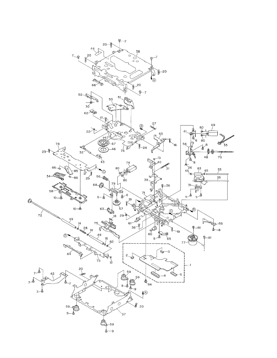
2.3 CD MECHANISM MODULE

11
DEH-1000,10,1050
Mark No. Description
Part No.
Mark No. Description
Part No.
1 Control Unit
CWX2344
2 Connector(CN802)
CKS2192
3 Connector(CN801)
CKS2193
4 Connector(CN701)
CKS2773
5 Connector(CN101)
CKS3486
6 Screw
BMZ20P030FZK
7 Screw
BSZ20P040FZK
8 Screw(M2
×
3)
CBA1077
9 Screw(M2
×
6)
CBA1230
10 Screw
CBA1243
11 Screw(M2
×
4)
CBA1362
12 Washer
CBF1037
13 Washer
CBF1038
14 Washer
CBF1060
*
15 Washer
CBF1075
16 Spring
CBH2079
17 Spring
CBH2117
18 Spring
CBH2082
19 Spring
CBH2110
20 Spring
CBH2111
21 Spring
CBH2114
22 Spring
CBH2115
23 Spring
CBH2080
24 Spring
CBH2118
25 Spring
CBH2161
26 Spring
CBH2163
27 Spring
CBH2189
28 Spring
CBH2249
29 Spring
CBH2260
30 Spring
CBH2262
31 Spring
CBL1367
32 Spring
CBL1369
33 Connector
CDE5531
34 Connector
CDE5532
35 Shaft
CLA3304
36 Screw(M2.6
×
6)
CBA1458
37 Frame
CNC7544
38 Frame
CNC7545
39 Lever
CNC7546
40 Arm
CNC7739
41 Bracket
CNC7798
42 Plate
CNC8090
43 Spacer
CNM3315
44 Sheet
CNM6170
45 Cushion
CNM6204
46 Sheet
CNM6215
47 Ball
CNR1189
48 Belt
CNT1086
49 Roller
CNV4509
50 Arm
CNV5246
51 Arm
CNV5247
52 Arm
CNV5248
53 Arm
CNV5249
54 Guide
CNV5254
55 Guide
CNV5255
56 Gear
CNV5257
57 Gear
CNV5256
58 Guide
CNV5259
59 Damper
CNV5266
60 Arm
CNV5359
61 Arm
CNV5360
62 Arm
CNV5361
63 Guide
CNV5509
64 Guide
CNV5510
65 Holder
CNV5578
66 Guide
CNV5751
67 Clamper
CNV5758
68 Gear
CNV5813
69 Motor Unit(M1)
CXB2190
70 Screw Unit
CXB2191
71 Chassis Unit
CXB2192
72 Gear Unit
CXB2193
73 Arm Unit
CXB2194
74 Motor Unit(M2)
CXB2195
75 Lever Unit
CXB2553
76 Arm Unit
CXB2554
77 Motor Unit(M3)
CXB2562
78 Arm Unit
CXB2795
79 Bracket Unit
CXB4071
80 Screw
JFZ20P025FMC
81 Screw
JGZ17P025FZK
82 Washer
YE15FUC
83 Pickup Unit(Service)(P8) CXX1285
84 Screw
IMS26P030FMC
*
85 PCB
CNX2982
86 Photo-transistor(Q1, 2)
CPT230SX-TU
- CD MECHANISM MODULE SECTION PARTS LIST
12
DEH-1000,10,1050
1
2
3
4
1
2
3
4
D
C
B
A
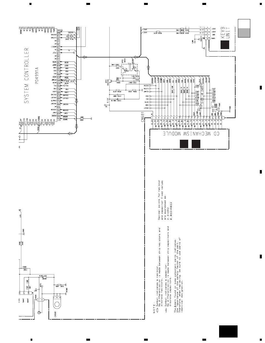
3. SCHEMATIC DIAGRAM
3.1 OVERALL CONNECTION DIAGRAM(GUIDE PAGE)
Note: When ordering service parts, be sure to refer to “EXPLODED VIEWS AND PARTS LIST” or “ELECTRICAL PARTS
LIST”.
A-a
A-b
A-a
A-a
A-b
A-b
A-b
A-b
A-a
A-a
Large size
SCH diagram
Guide page
Detailed page
A
A-a
ANTENNA
CABLE
A
A
B
E
D
13
DEH-1000,10,1050
5
6
7
8
5
6
7
8
D
C
B
A
A-b
A
RESET
CEK1136
DEH-P1000/X1N/UC
DEH-P10/X1N/UC
DEH-P1050/X1N/ES
R612
DELETED
47K
R613
0R0
DELETED
4.3V
4.3V
14
DEH-1000,10,1050
1
2
3
4
1
2
3
4
D
C
B
A
A
SOURCE SELECTOR, ELECTRONIC VOLUME
4.3V
4.3V
4.3V
4.3V
4.3V
4.3V
4.3V
A-a
A-a
A-b
A
B
17
DEH-1000,10,1050
5
6
7
8
5
6
7
8
D
C
B
A
CEK1136
R612
DELETED
47K
R613
0R0
DELETED
A-b
A-a
A-b
18
DEH-1000,10,1050
1
2
3
4
1
2
3
4
D
C
B
A
B
KV1410(23)
Voltage of IC Terminals
Mark
None
F0
F65
F125
A0
A74
A125
Band
–
FM
FM
FM
AM
AM
AM
Input Level
–
0dBf
65dBf
125dBf
0dB
µ
74dB
µ
125dB
µ
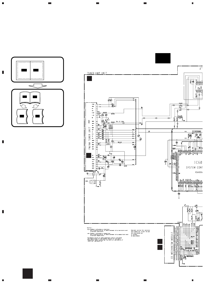
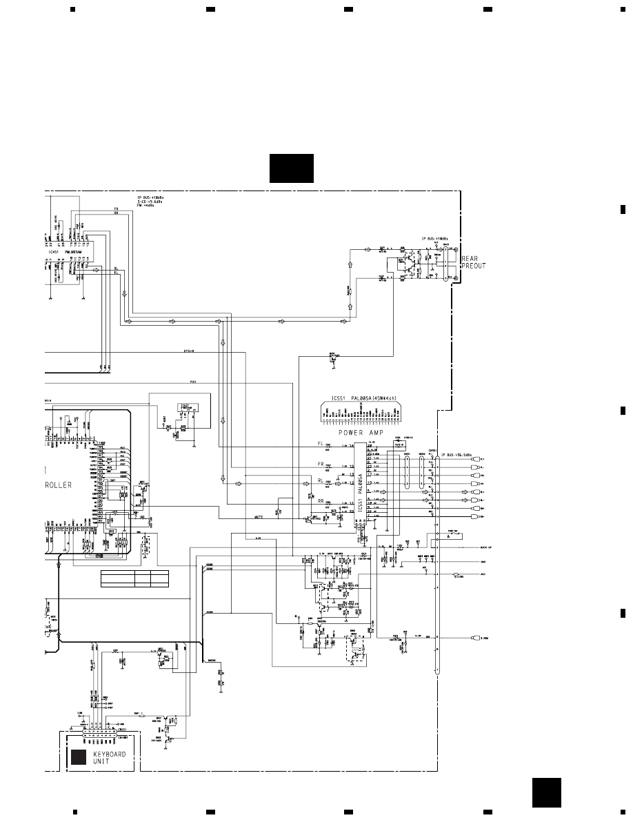
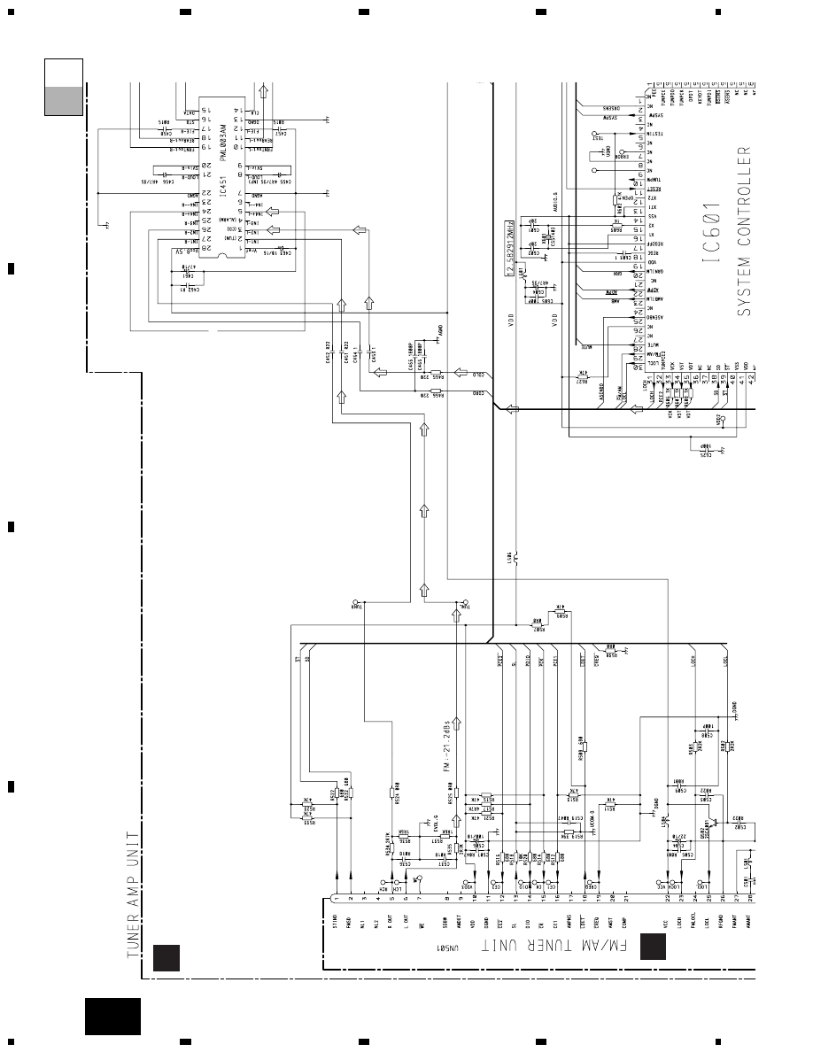
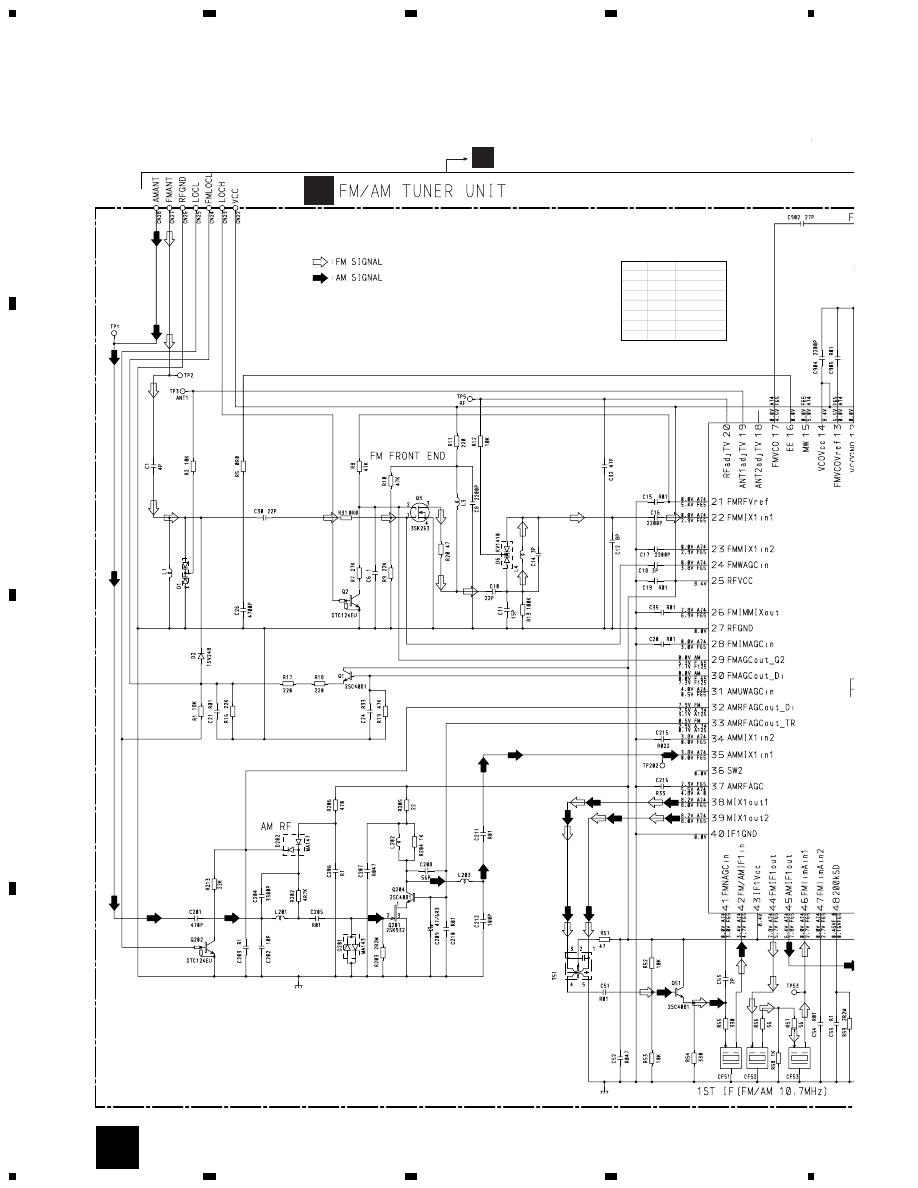
3.2 FM/AM TUNER UNIT
B
A
19
DEH-1000,10,1050
5
6
7
8
5
6
7
8
D
C
B
A
KV1410(23)
B
20
DEH-1000,10,1050
1
2
3
4
1
2
3
4
D
C
B
A
CLOCK
PGM
DEH-1000/X1N/UC
DEH-1050/X1N/ES
DEH-10/X1N/UC
IL1801-1805
CEL1549
CEL1508
C
3.3 KEYBOARD UNIT
C
A
CN651
KEYBOARD UNIT
DEH-1000,10,1050
1
2
3
4
1
2
3
4
D
C
B
A
PICKUP UNIT(SERVICE)
PHOTO UNIT
CONTROL UNIT
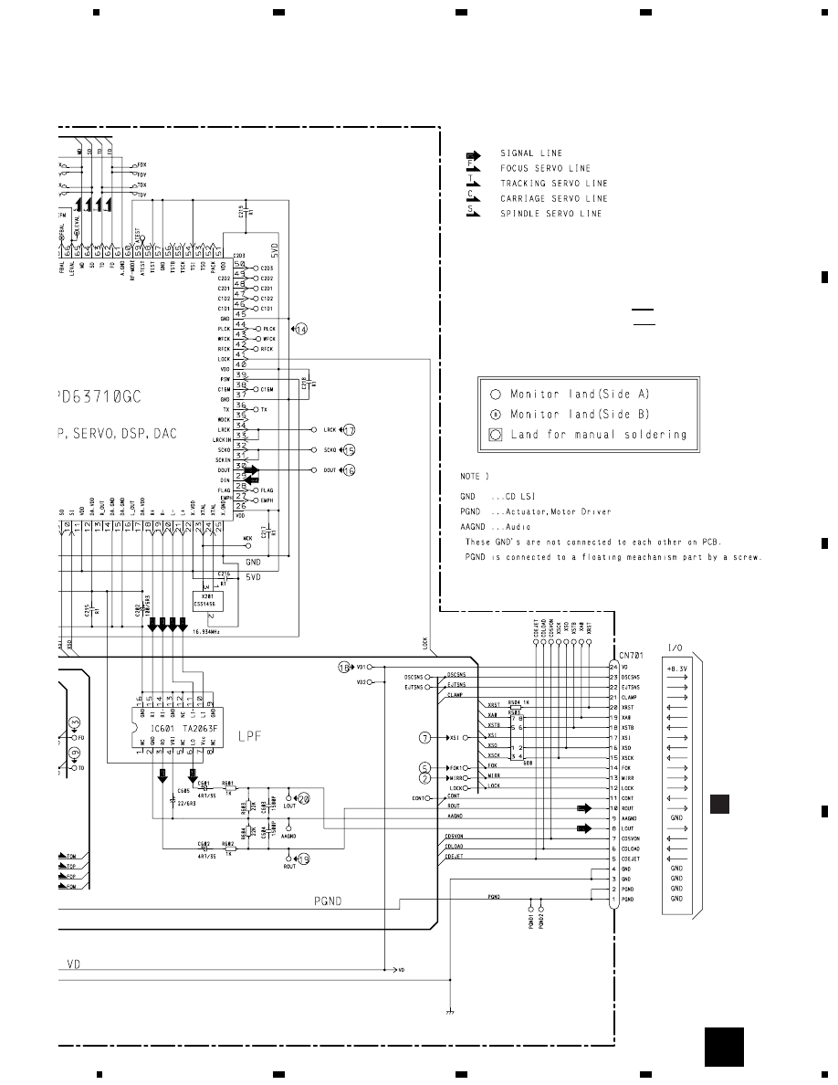
3.4 CD MECHANISM MODULE
D
22
E
D
E
DEH-1000,10,1050
5
6
7
8
5
6
7
8
D
C
B
A
SWITCHES:
CONTROL UNIT
S801 : HOME SWITCH.....ON-OFF
S802 : CLAMP SWITCH....ON-OFF
The underlined indicates the switch position.
23
D
A
CN681
24
DEH-1000,10,1050
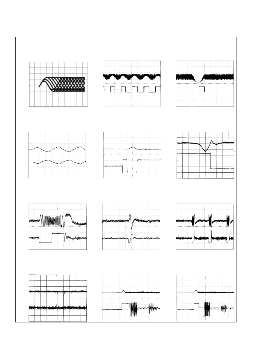
1 RFI
0.5V/div. 0.5
µ
s/div.
Normal mode: play
1 CH1: RFI
1V/div.
2 CH2: MIRR
5V/div.
Test mode: Tracking open
0.5ms/div.
1 CH1: RFI
1V/div.
2 CH2: MIRR
5V/div.
Normal mode: The defect part
passes 800
µ
m
0.5ms/div.
3 CH1: FD
0.5V/div.
4 CH2: FO+
2V/div.
Test mode: No disc, Focus close
0.2s/div.
3 CH1: FD
0.5V/div.
5 CH2: FOK
2V/div.
Normal mode: Focus close
0.2s/div.
6 CH1: FE
0.5V/div.
7 CH2: XSI
2V/div.
Normal mode: Focus close
1ms/div.
REFO
→
8 CH1: TE
0.5V/div.
9 CH2: TD
0.5V/div.
Test mode: 32 tracks jump (REV)
0.5ms/div.
8 CH1: TE
0.5V/div.
9 CH2: TD
0.5V/div.
Test mode: Single jump (REV)
0.5ms/div.
8 CH1: TE
0.5V/div.
9 CH2: TD
0.5V/div.
Test mode: 100 tracks jump (REV)
5ms/div.
6 CH1: FE
0.1V/div.
3 CH2: FD
0.2V/div.
Normal mode: Play
20ms/div.
3 CH1: FD
0.5V/div.
0 CH2: MD
1V/div.
Normal mode: Focus close (12cm)
0.5s/div.
3 CH1: FD
0.5V/div.
0 CH2: MD
1V/div.
Normal mode: Focus close (8cm)
0.5s/div.
REFO
→
REFO
→
REFO
→
REFO
→
REFO
→
REFO
→
GND
→
REFO
→
REFO
→
REFO
→
REFO
→
REFO
→
REFO
→
REFO
→
REFO
→
REFO
→
REFO
→
REFO
→
REFO
→
- Waveforms
Note:1. The encircled numbers denote measuring pointes in the circuit diagram.
2. Reference voltage
REFO:2.5V
REFO
→
REFO
→
REFO
→
REFO
→
25
DEH-1000,10,1050
8 CH1: TE
0.2V/div.
9 CH2: TD
0.2V/div.
Normal mode: play
8 CH1: TE
0.5V/div.
! CH2: SD
0.5V/div.
TEST mode: 100 Tracks jump(FWD)
5ms/div.
0 MD
0.5V/div.
0.1s/div.
Normal mode: Play (12cm)
0 MD
1V/div.
10ms/div.
Normal mode:
Long Search (12cm)
@ EFM
1V/div.
5
µ
s/div.
Normal mode: play
8 CH1: TE
1V/div.
# CH2: TEC
1V/div.
Test mode: Focus close
Tracking open
2ms/div.
8 CH1: TE
0.5V/div.
6 CH2: FE
0.5V/div.
Normal mode: AGC after focus close
0.2s/div.
$ PLCK
2V/div.
0.5
µ
s/div.
Normal mode: play
20ms/div.
% SCKO
2V/div.
1
µ
s/div.
Normal mode: play
^ Dout
2V/div.
10
µ
s/div.
Normal mode: play
& LRCK
2V/div.
20
µ
s/div.
Normal mode: play
* VD
5V/div.
50ms/div.
Normal mode: No disc
GND
→
REFO
→
REFO
→
GND
→
REFO
→
REFO
→
REFO
→
REFO
→
REFO
→
REFO
→
REFO
→
REFO
→
REFO
→
GND
→
REFO
→
GND
→
REFO
→
GND
→
REFO
→
GND
→
REFO
→
26
DEH-1000,10,1050
( CH1: R OUT
1V/div.
) CH2: L OUT
1V/div.
Normal mode: Play (1kHz 0dB)
6 CH1: FE
0.2V/div.
3 CH2: FD
0.5V/div.
Normal mode: During AGC
1ms/div.
8 CH1: TE
0.2V/div.
9 CH2: TD
0.5V/div.
Normal mode: During AGC
1 CH1: RFI
1V/div.
⁄ CH2: HOLD
5V/div.
Normal mode: The defect part passes
800
µ
m(B.D)
0.2ms/div.
1ms/div.
0.5ms/div.
3 CH1: FD
1V/div.
⁄ CH2: HOLD 5V/div.
Normal mode: The defect part passes
800
µ
m(B.D)
0.5ms/div.
9 CH1: TD
0.1V/div.
⁄ CH2: HOLD 5V/div.
Normal mode: The defect part passes
800
µ
m(B.D)
0.5ms/div.
REFO
→
REFO
→
REFO
→
REFO
→
REFO
→
REFO
→
REFO
→
REFO
→
REFO
→
REFO
→
REFO
→
REFO
→

27
DEH-1000,10,1050
28
DEH-1000,10,1050
1
2
3
4
1
2
3
4
D
C
B
A
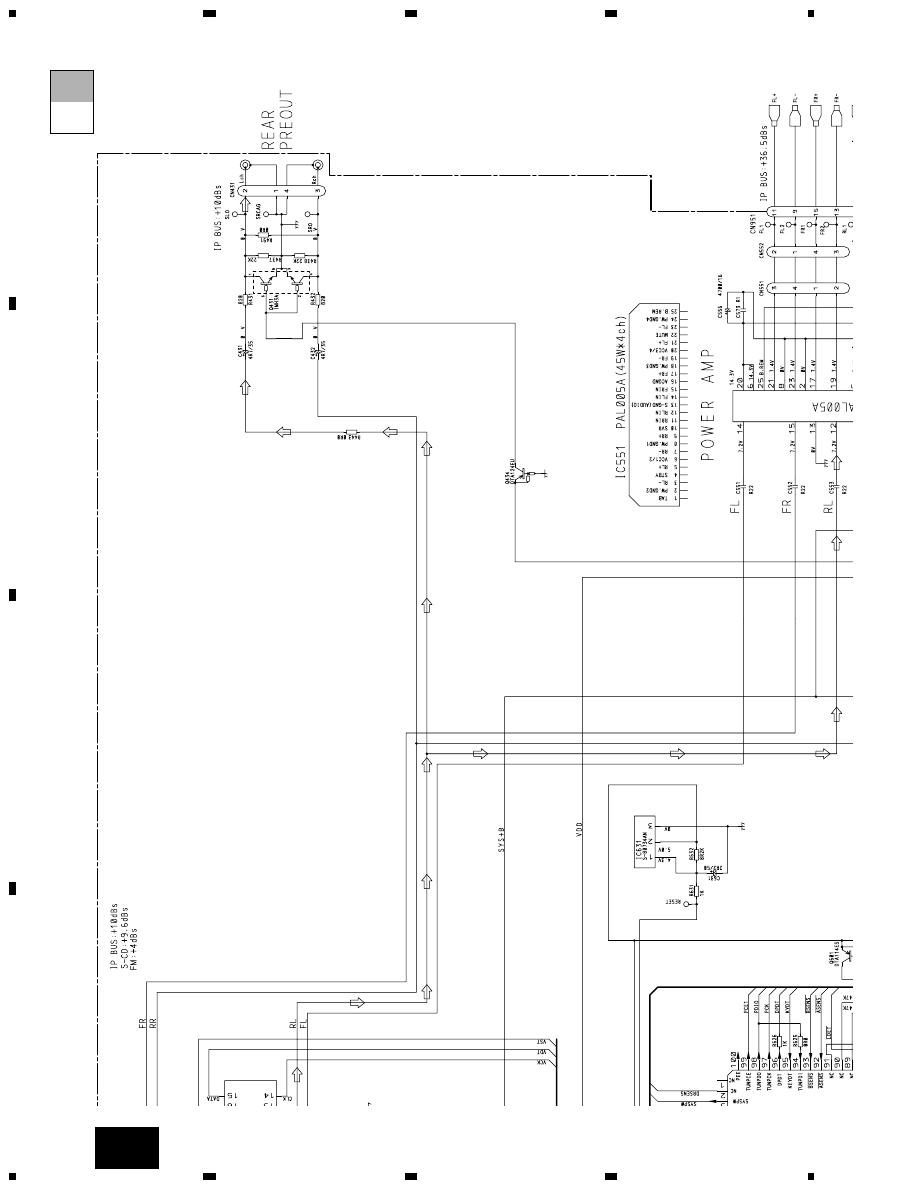
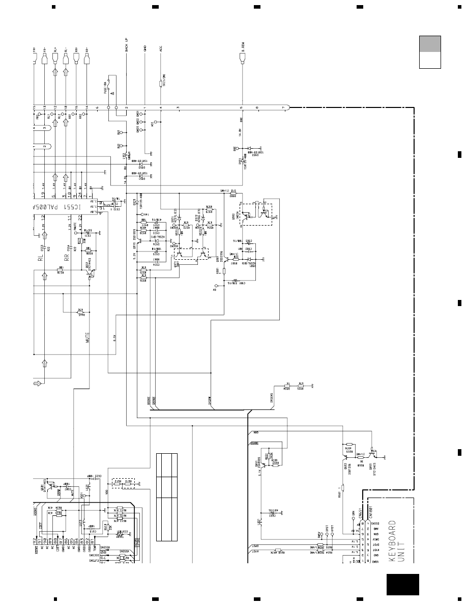
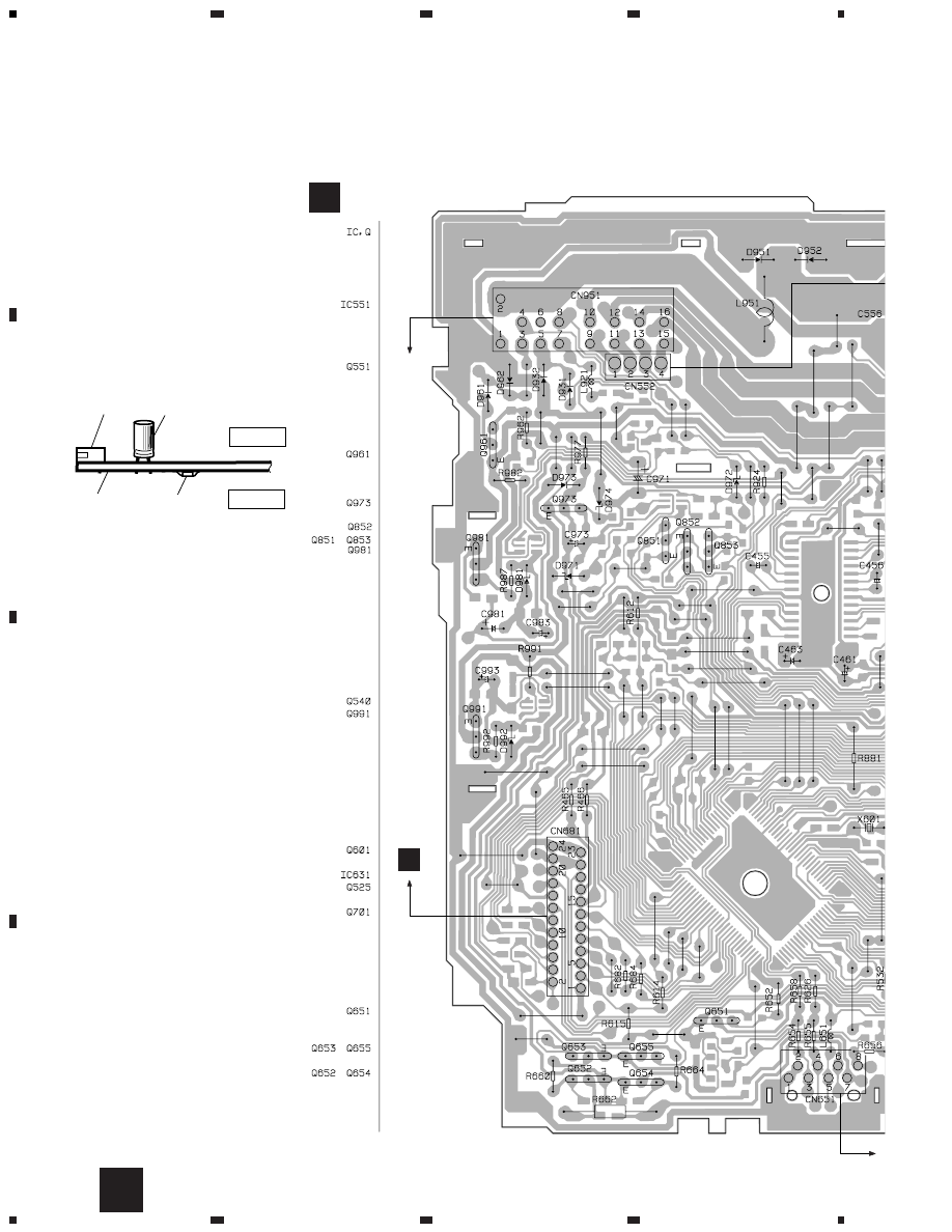
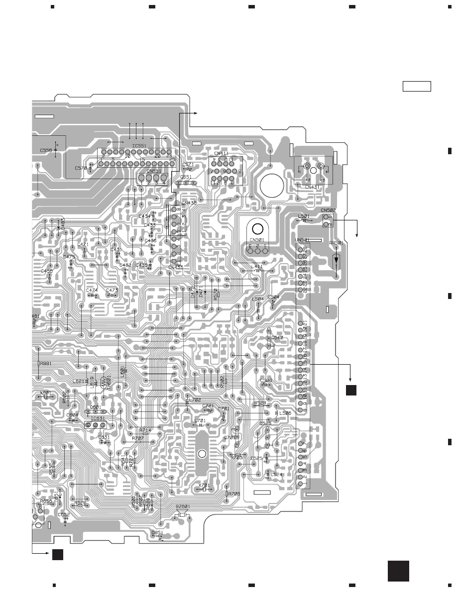
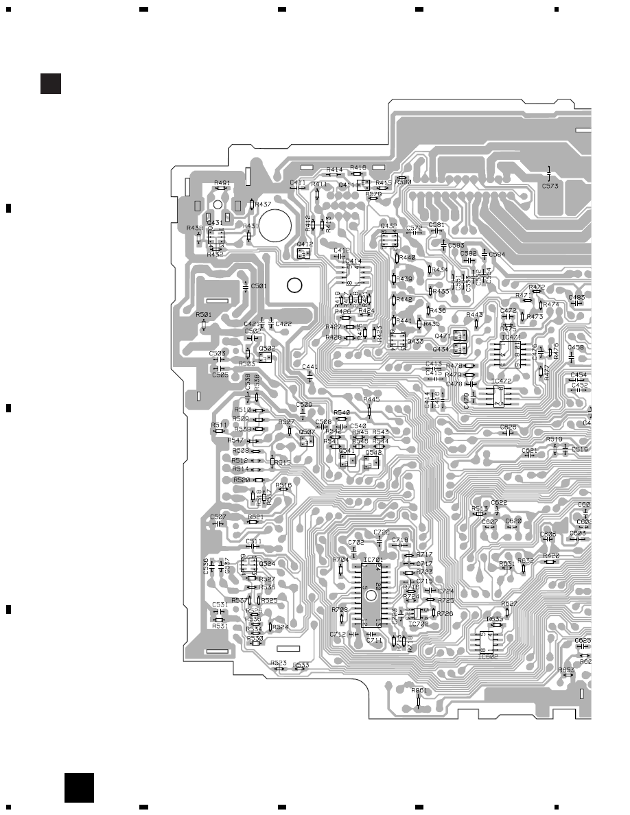
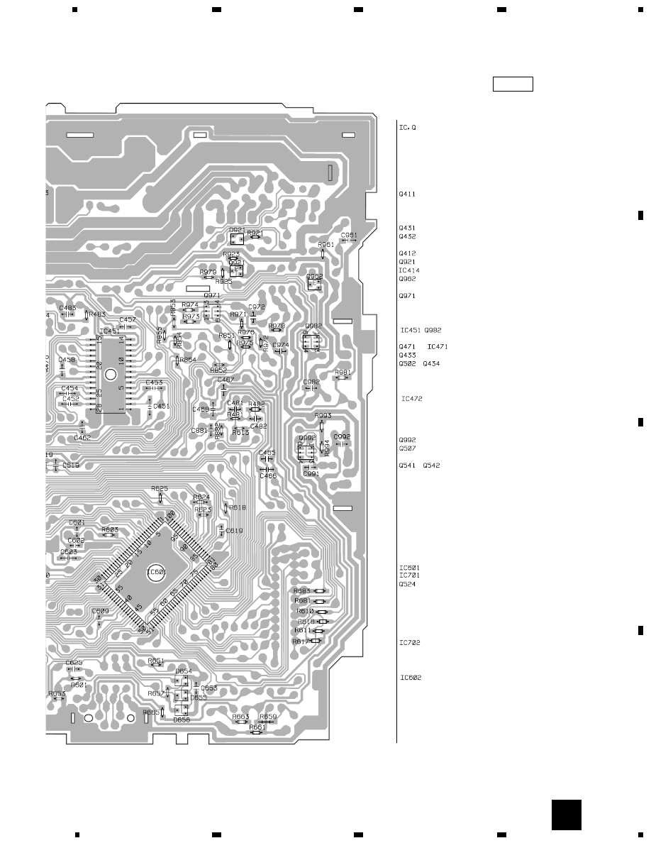
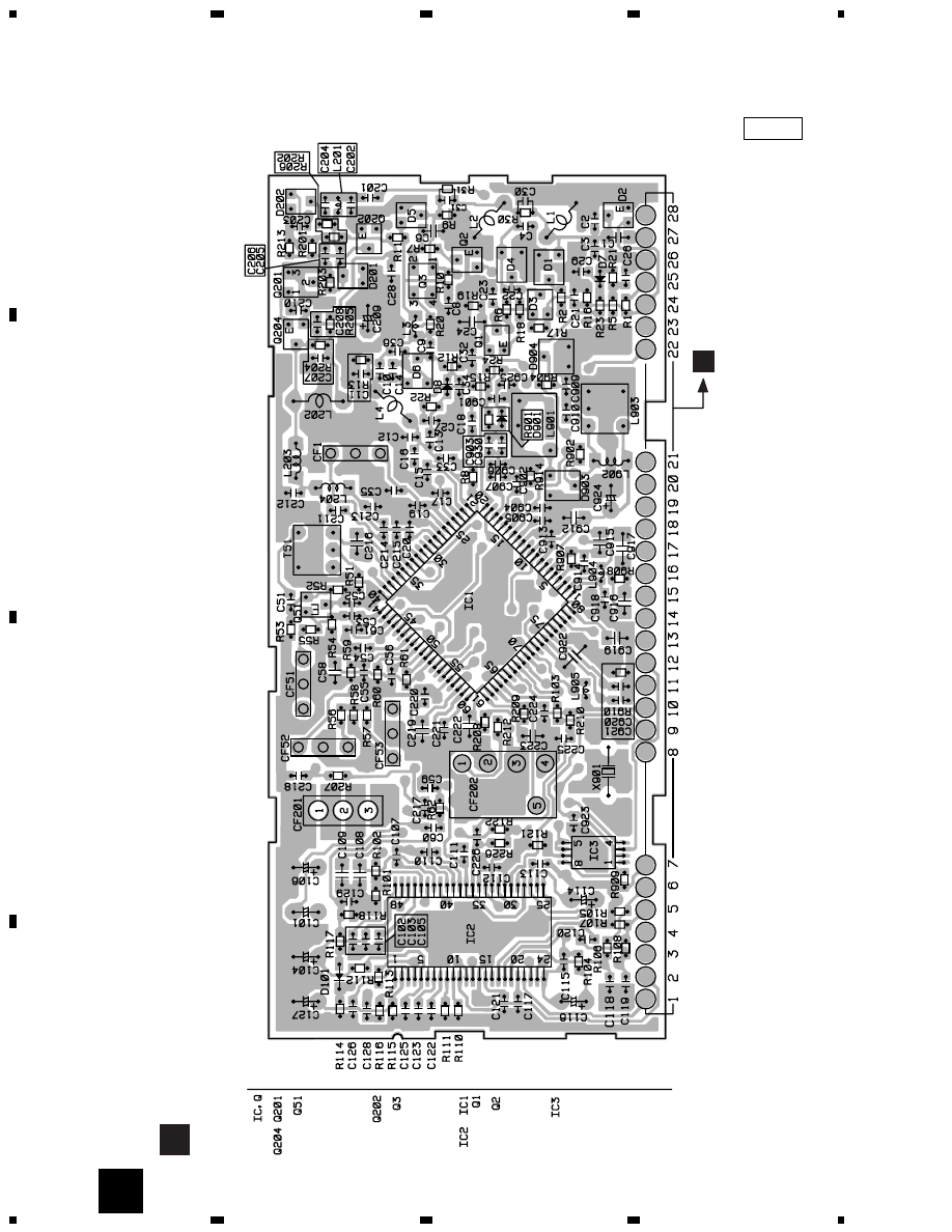
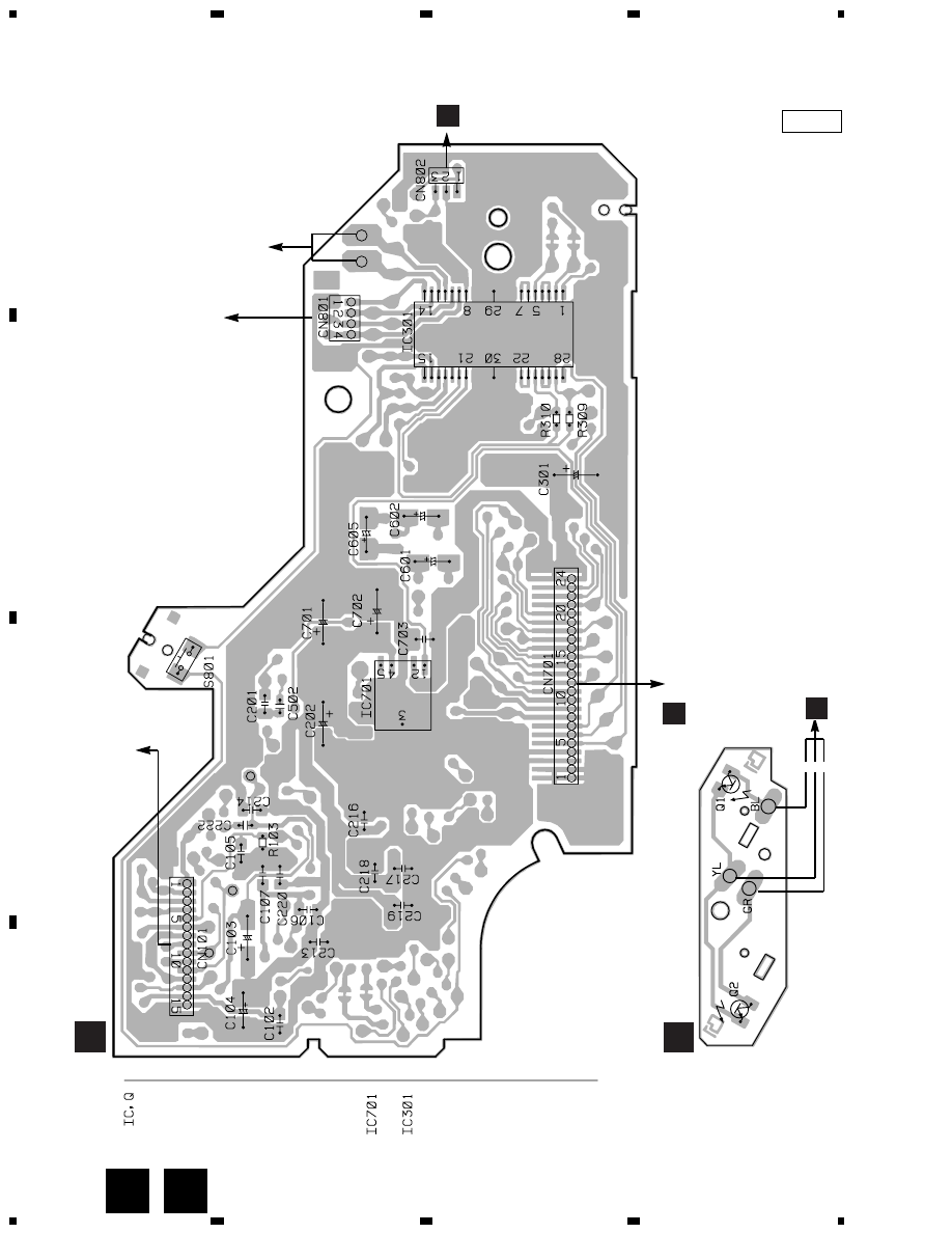
4. PCB CONNECTION DIAGRAM
4.1 TUNER AMP UNIT
NOTE FOR PCB DIAGRAMS
1. The parts mounted on this PCB
include all necessary parts for
several destination.
For further information for
respective destinations, be sure
to check with the schematic dia-
gram.
2. Viewpoint of PCB diagrams
A
A
Capacitor
Connector
P.C.Board
Chip Part
SIDE A
SIDE B
TUNER AMP UNIT
CORD ASSY
CN701
D
29
DEH-1000,10,1050
5
6
7
8
5
6
7
8
D
C
B
A
A
L ch
R ch
SUB WOOFER/
REAR PREOUT
IP BUS IN
SIDE A
B
ANTENNA CABLE
30
DEH-1000,10,1050
1
2
3
4
1
2
3
4
D
C
B
A
A
A
TUNER AMP UNIT
31
DEH-1000,10,1050
5
6
7
8
5
6
7
8
D
C
B
A
A
SIDE B
32
DEH-1000,10,1050
1
2
3
4
1
2
3
4
D
C
B
A
4.2 FM/AM TUNER UNIT
B
B
SIDE A
FM/AM TUNER UNIT
A
33
DEH-1000,10,1050
1
2
3
4
1
2
3
4
D
C
B
A
B
B
SIDE B
FM/AM TUNER UNIT
34
DEH-1000,10,1050
1
2
3
4
1
2
3
4
D
C
B
A
4.3 KEYBOARD UNIT
VOL
UP
EQ+
VOL
DOWN
EQ–
SOURCE
DISPLAY
1
2
3
4
5
6
TA,PGM
PTY,CLOCK
BAND
EJECT
FUNC
←
AUDIO
←
←
←
C
C
SIDE A
KEYBOARD UNIT
35
DEH-1000,10,1050
1
2
3
4
1
2
3
4
D
C
B
A
C
C
SIDE B
KEYBOARD UNIT
A
CN651
36
DEH-1000,10,1050
1
2
3
4
1
2
3
4
D
C
B
A
4.4 CD MECHANISM MODULE
CONTROL UNIT
E
REFO
F
M1 CARRIAGE MOTOR
M2 LOADING MOTOR
M3 SPINDLE MOTOR
PICKUP UNIT(SER
VICE)
CN802
CN681
3 2 1
PHOTO UNIT
SIDE A
A
D
E
D
D E
E
37
DEH-1000,10,1050
D
C
B
A
1
2
3
4
1
2
3
4
CONTROL UNIT
SIDE B
D
D

38
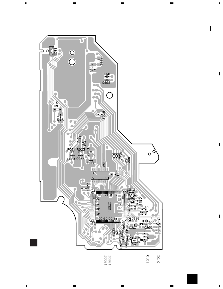
DEH-1000,10,1050
5. ELECTRICAL PARTS LIST
NOTES:
- Parts whose parts numbers are omitted are subject to being not supplied.
- The part numbers shown below indicate chip components.
Chip Resistor
RS1/_S___J,RS1/__S___J
Chip Capacitor (except for CQS.....)
CKS....., CCS....., CSZS.....
=====Circuit Symbol and No.===Part Name
Part No.
---
------
------------------------------------------
-------------------------
Unit Number : CWM6092(DEH-1000/X1N/UC,10/X1N/UC)
Unit Name
: Tuner Amp Unit
MISCELLANEOUS
IC
451
IC
PML003AM
IC
551
IC
PAL005A
IC
601
IC
PD4991A
IC
631
IC
S-80734AN
Q
431
Transistor
IMH3A
Q
434
Transistor
DTA124EU
Q
502
Transistor
2SC4081
Q
551
Transistor
DTC144ES
Q
601
Transistor
DTA114ES
Q
651
Transistor
2SA933S
Q
652
Transistor
2SB1236
Q
653
Transistor
DTC124ES
Q
971
Transistor
IMX1
Q
973
Transistor
2SD1859
Q
981
Transistor
2SD2396
Q
982
Transistor
IMD2A
Q
991
Transistor
2SD2396
Q
992
Transistor
IMD2A
D
931
Diode
1SR139-400
D
932
Diode
1SR139-400
D
951
Diode
1SR139-400
D
952
Diode
1SR139-400
D
971
Diode
HZS7L(C2)
D
972
Diode
HZS6L(C3)
D
973
Diode
1SR139-400
D
974
Diode
HZS6L(B1)
D
981
Diode
HZS9L(B3)
D
992
Diode
HZS9L(B1)
L
501
Ferri-Inductor
LAU4R7K
L
504
Ferri-Inductor
LAU2R2K
L
506
Inductor
LAU100K
L
601
Inductor
LAU100K
L
619
Ferri-Inductor
LAU2R2K
L
621
Ferri-Inductor
LAU2R2K
L
651
Ferri-Inductor
LAU101K
L
951
Choke Coil 600µH
CTH1221
TH
601
Thermistor
CCX1031
X
601
Radiator 12.58291MHz
CSS1402
FM/AM Tuner Unit
CWE1501
AR
501
DSP-201M
RESISTORS
R
421
RS1/10S473J
R
431
RS1/10S821J
R
432
RS1/10S821J
R
437
RS1/10S223J
R
438
RS1/10S223J
R
443
RS1/10S0R0J
R
445
RS1/8S473J
R
465
RD1/4PU221J
R
466
RD1/4PU221J
R
501
RS1/10S0R0J
R
502
RD1/4PU222J
R
503
RS1/10S222J
R
507
RS1/10S0R0J
R
508
RS1/10S681J
R
509
RS1/10S473J
R
511
RS1/10S473J
R
512
RS1/10S681J
R
513
RS1/8S473J
R
514
RS1/10S681J
R
515
RS1/8S473J
R
516
RS1/10S681J
R
517
RS1/8S472J
R
518
RS1/10S103J
R
519
RS1/10S393J
R
520
RS1/10S681J
R
521
RS1/10S473J
R
522
RD1/4PU681J
R
523
RS1/10S473J
R
524
RS1/10S0R0J
R
525
RS1/10S0R0J
R
532
RD1/4PU681J
R
533
RS1/10S473J
R
534
RS1/10S272J
R
535
RS1/10S272J
R
536
RS1/10S162J
R
537
RS1/10S162J
R
538
RS1/10S0R0J
R
570
RD1/4PU103J
R
579
RS1/10S331J
R
580
RS1/10S103J
R
601
RS1/10S0R0J
R
602
RD1/4PU473J
R
603
RS1/10S102J
R
606
RD1/4PU102J
R
607
RD1/4PU102J
R
608
RD1/4PU102J
R
610
RS1/10S222J
R
611
RS1/10S473J
R
613
RS1/10S0R0J
R
614
RD1/4PU222J
R
615
RD1/4PU473J
R
616
RS1/10S222J
R
617
RS1/10S473J
R
618
RN1/10SE2002D
R
623
RS1/10S473J
R
624
RS1/8S473J
R
625
RS1/10S0R0J
R
626
RD1/4PU102J
R
627
RS1/10S473J
R
631
RS1/10S102J
R
632
RS1/10S822J
R
651
RS1/10S222J
R
652
RD1/4PU472J
R
654
RD1/4PU222J
R
655
RD1/4PU222J
=====Circuit Symbol and No.===Part Name
Part No.
---
------
------------------------------------------
-------------------------
A

39
DEH-1000,10,1050
R
658
RD1/4PU472J
R
659
RS1/8S472J
R
660
RD1/4PU302J
R
661
RS1/10S1R0J
R
681
RS1/10S681J
R
682
RD1/4PU102J
R
683
RS1/10S102J
R
684
RD1/4PU102J
R
924
RD1/4PU102J
R
925
RS1/10S473J
R
971
RS1/10S103J
R
972
RS1/10S473J
R
973
RS1/10S103J
R
974
RS1/10S473J
R
975
RS1/10S473J
R
976
RS1/10S473J
R
977
RD1/4PU101J
R
978
RS1/10S472J
R
979
RS1/10S472J
R
981
RS1/10S1R0J
R
982
RD1/4PU511J
R
987
RD1/4PU221J
R
991
RD1/4PU221J
R
992
RD1/4PU221J
R
993
RS1/10S472J
R
994
RS1/10S222J
CAPACITORS
C
431
CEJA4R7M35
C
432
CEAL4R7M35
C
451
CKSYB224K25
C
452
CKSYB224K25
C
453
CKSYB105K16
C
454
CKSYB105K16
C
455
CEJANP4R7M16
C
456
CEJANP4R7M16
C
457
CKSQYB153K50
C
458
CKSQYB153K50
C
461
CEAL470M10
C
462
CKSQYB104K25
C
463
CEJA100M16
C
465
CCSQSL182J50
C
466
CCSSL182J50
C
501
CKSQYB103K50
C
502
CKSQYB223K50
C
503
CKSQYB223K50
C
504
CEJA220M10
C
505
CKSQYB102K50
C
506
CEAL101M10
C
507
CKSQYB473K25
C
508
CCSQCH101J50
C
509
CKSQYB102K50
C
519
CKSQYB472K50
C
536
CKSQYB183K50
C
537
CKSQYB183K50
C
551
CKSYB224K25
C
552
CKSYB224K25
C
553
CKSYB224K25
C
554
CKSYB224K25
C
556
4700µF/16V
CCH1328
C
570
CEJA100M16
C
571
CEJA330M10
C
572
CKSYB105K16
C
573
CKSYB104K50
C
601
CCSQCH200J50
C
602
CCSQCH200J50
C
603
CKSYB105K16
C
604
CEJA4R7M35
C
605
CCSQCH101J50
C
607
CCSQCH101J50
C
619
CCSQCH101J50
C
622
CCSQCH101J50
C
625
CCSQCH101J50
C
631
CEJA2R2M50
C
652
CEJA4R7M35
C
971
470µF/16V
CCH1331
C
972
CKSQYB473K25
C
973
CEJA101M10
C
974
CKSQYB473K25
C
981
330µF/16V
CCH1326
C
982
CKSQYB103K50
C
983
CEJA101M16
C
991
CKSQYB473K25
C
992
CKSQYB102K50
C
993
CEJA101M10
Unit Number : CWM6093(DEH-1050/X1N/ES)
Unit Name
: Tuner Amp Unit
MISCELLANEOUS
IC
451
IC
PML003AM
IC
551
IC
PAL005A
IC
601
IC
PD4991A
IC
631
IC
S-80734AN
Q
431
Transistor
IMH3A
Q
434
Transistor
DTA124EU
Q
502
Transistor
2SC4081
Q
551
Transistor
DTC144ES
Q
601
Transistor
DTA114ES
Q
651
Transistor
2SA933S
Q
652
Transistor
2SB1236
Q
653
Transistor
DTC124ES
Q
971
Transistor
IMX1
Q
973
Transistor
2SD1859
Q
981
Transistor
2SD2396
Q
982
Transistor
IMD2A
Q
991
Transistor
2SD2396
Q
992
Transistor
IMD2A
D
931
Diode
1SR139-400
D
932
Diode
1SR139-400
D
951
Diode
1SR139-400
D
952
Diode
1SR139-400
D
971
Diode
HZS7L(C2)
D
972
Diode
HZS6L(C3)
D
973
Diode
1SR139-400
D
974
Diode
HZS6L(B1)
D
981
Diode
HZS9L(B3)
D
992
Diode
HZS9L(B1)
L
501
Ferri-Inductor
LAU4R7K
L
504
Ferri-Inductor
LAU2R2K
L
506
Inductor
LAU100K
L
601
Inductor
LAU100K
L
619
Ferri-Inductor
LAU2R2K
L
621
Ferri-Inductor
LAU2R2K
L
651
Ferri-Inductor
LAU101K
L
951
Choke Coil 600µH
CTH1221
TH
601
Thermistor
CCX1031
X
601
Radiator 12.58291MHz
CSS1402
FM/AM Tuner Unit
CWE1501
AR
501
DSP-201M
RESISTORS
R
421
RS1/10S473J
R
431
RS1/10S821J
R
432
RS1/10S821J
R
437
RS1/10S223J
R
438
RS1/10S223J
=====Circuit Symbol and No.===Part Name
Part No.
---
------
------------------------------------------
-------------------------
=====Circuit Symbol and No.===Part Name
Part No.
---
------
------------------------------------------
-------------------------
A

40
DEH-1000,10,1050
R
443
RS1/10S0R0J
R
445
RS1/8S473J
R
465
RD1/4PU221J
R
466
RD1/4PU221J
R
501
RS1/10S0R0J
R
502
RD1/4PU222J
R
503
RS1/10S222J
R
507
RS1/10S0R0J
R
508
RS1/10S681J
R
509
RS1/10S473J
R
511
RS1/10S473J
R
512
RS1/10S681J
R
513
RS1/8S473J
R
514
RS1/10S681J
R
515
RS1/8S473J
R
516
RS1/10S681J
R
517
RS1/8S472J
R
518
RS1/10S103J
R
519
RS1/10S393J
R
520
RS1/10S681J
R
521
RS1/10S473J
R
522
RD1/4PU681J
R
523
RS1/10S473J
R
524
RS1/10S0R0J
R
525
RS1/10S0R0J
R
532
RD1/4PU681J
R
533
RS1/10S473J
R
534
RS1/10S272J
R
535
RS1/10S272J
R
536
RS1/10S162J
R
537
RS1/10S162J
R
538
RS1/10S0R0J
R
570
RD1/4PU103J
R
579
RS1/10S331J
R
580
RS1/10S103J
R
601
RS1/10S0R0J
R
602
RD1/4PU473J
R
603
RS1/10S102J
R
606
RD1/4PU102J
R
607
RD1/4PU102J
R
608
RD1/4PU102J
R
610
RS1/10S222J
R
611
RS1/10S473J
R
612
RD1/4PU473J
R
614
RD1/4PU222J
R
615
RD1/4PU473J
R
616
RS1/10S222J
R
617
RS1/10S473J
R
618
RN1/10SE2002D
R
623
RS1/10S473J
R
624
RS1/8S473J
R
625
RS1/10S0R0J
R
626
RD1/4PU102J
R
627
RS1/10S473J
R
631
RS1/10S102J
R
632
RS1/10S822J
R
651
RS1/10S222J
R
652
RD1/4PU472J
R
654
RD1/4PU222J
R
655
RD1/4PU222J
R
658
RD1/4PU472J
R
659
RS1/8S472J
R
660
RD1/4PU302J
R
661
RS1/10S1R0J
R
681
RS1/10S681J
R
682
RD1/4PU102J
R
683
RS1/10S102J
R
684
RD1/4PU102J
R
924
RD1/4PU102J
R
925
RS1/10S473J
R
971
RS1/10S103J
R
972
RS1/10S473J
R
973
RS1/10S103J
R
974
RS1/10S473J
R
975
RS1/10S473J
R
976
RS1/10S473J
R
977
RD1/4PU101J
R
978
RS1/10S472J
R
979
RS1/10S472J
R
981
RS1/10S1R0J
R
982
RD1/4PU511J
R
987
RD1/4PU221J
R
991
RD1/4PU221J
R
992
RD1/4PU221J
R
993
RS1/10S472J
R
994
RS1/10S222J
CAPACITORS
C
431
CEJA4R7M35
C
432
CEAL4R7M35
C
451
CKSYB224K25
C
452
CKSYB224K25
C
453
CKSYB105K16
C
454
CKSYB105K16
C
455
CEJANP4R7M16
C
456
CEJANP4R7M16
C
457
CKSQYB153K50
C
458
CKSQYB153K50
C
461
CEAL470M10
C
462
CKSQYB104K25
C
463
CEJA100M16
C
465
CCSQSL182J50
C
466
CCSSL182J50
C
501
CKSQYB103K50
C
502
CKSQYB223K50
C
503
CKSQYB223K50
C
504
CEJA220M10
C
505
CKSQYB102K50
C
506
CEAL101M10
C
507
CKSQYB473K25
C
508
CCSQCH101J50
C
509
CKSQYB102K50
C
519
CKSQYB472K50
C
536
CKSQYB183K50
C
537
CKSQYB183K50
C
551
CKSYB224K25
C
552
CKSYB224K25
C
553
CKSYB224K25
C
554
CKSYB224K25
C
556
4700µF/16V
CCH1328
C
570
CEJA100M16
C
571
CEJA330M10
C
572
CKSYB105K16
C
573
CKSYB104K50
C
601
CCSQCH200J50
C
602
CCSQCH200J50
C
603
CKSYB105K16
C
604
CEJA4R7M35
C
605
CCSQCH101J50
C
607
CCSQCH101J50
C
619
CCSQCH101J50
C
622
CCSQCH101J50
C
625
CCSQCH101J50
=====Circuit Symbol and No.===Part Name
Part No.
---
------
------------------------------------------
-------------------------
=====Circuit Symbol and No.===Part Name
Part No.
---
------
------------------------------------------
-------------------------

41
DEH-1000,10,1050
C
631
CEJA2R2M50
C
652
CEJA4R7M35
C
971
470µF/16V
CCH1331
C
972
CKSQYB473K25
C
973
CEJA101M10
C
974
CKSQYB473K25
C
981
330µF/16V
CCH1326
C
982
CKSQYB103K50
C
983
CEJA101M16
C
991
CKSQYB473K25
C
992
CKSQYB102K50
C
993
CEJA101M10
Unit Number : CWE1501
Unit Name
: FM/AM Tuner Unit
CAPACITORS
IC
1
IC
PML002A
IC
2
IC
PM4008A
IC
3
IC
BR9010FV
Q
1
Transistor
2SC4081
Q
2
Transistor
DTC124EU
Q
3
FET
3SK263
Q
51
Transistor
2SC4081
Q
201
FET
2SK932
Q
202
Transistor
DTC124EU
Q
204
Transistor
2SC4081
D
1
Diode
KV1410(23)
D
2
Diode
1SV248
D
6
Diode
KV1410(23)
D
201
Diode
MA143
D
202
Diode
MA147
D
903
Diode
KV1410(23)
D
904
Diode
SVC253
L
1
Coil
CTC1155
L
3
Inductor
LCTB1R5K2125
L
4
Coil
CTC1155
L
201
Inductor
LCTB330K1608
L
202
Inductor
CTF1287
L
203
Inductor
LCTA121J3225
L
901
Coil
CTC1154
L
902
Inductor
LCTA3R3J3225
L
904
Inductor
LCTBR47K1608
L
905
Inductor
LCTBR47K1608
T
51
Coil
CTE1132
CF
51
Ceramic Filter
CTF1442
CF
52
Ceramic Filter
CTF1442
CF
53
Ceramic Filter
CTF1442
CF
202
Ceramic Filter
CTF1348
X
901
Crystal Resonator 10.250MHz
CSS1432
RESISTORS
R
1
RS1/16S183J
R
2
RS1/16S103J
R
5
RS1/16S0R0J
R
7
RS1/16S273J
R
8
RS1/16S473J
R
9
RS1/16S223J
R
10
RS1/16S473J
R
11
RS1/16S221J
R
12
RS1/16S103J
R
13
RS1/16S104J
R
16
RS1/16S223J
R
17
RS1/16S221J
R
18
RS1/16S221J
R
19
RS1/16S473J
R
20
RS1/16S470J
R
31
RS1/16S0R0J
R
51
RS1/16S470J
R
52
RS1/16S103J
R
53
RS1/16S103J
R
54
RS1/16S331J
R
55
RS1/16S331J
R
56
RS1/16S560J
R
57
RS1/16S560J
R
58
RS1/16S102J
R
59
RS1/16S225J
R
60
RS1/16S133J
R
61
RS1/16S433J
R
101
RS1/16S333J
R
102
RS1/16S103J
R
103
RS1/16S333J
R
104
RS1/16S562J
R
106
RS1/16S0R0J
R
108
RS1/16S0R0J
R
110
RS1/16S154J
R
111
RS1/16S273J
R
113
RS1/16S222J
R
114
RS1/16S333J
R
115
RS1/16S334J
R
116
RS1/16S473J
R
202
RS1/16S472J
R
203
RS1/16S225J
R
204
RS1/16S102J
R
205
RS1/16S220J
R
206
RS1/16S471J
R
208
RS1/16S104J
R
209
RS1/16S104J
R
210
RS1/16S563J
R
213
RS1/16S223J
R
902
RS1/16S103J
R
904
RS1/16S473J
R
907
RS1/16S103J
R
908
RS1/16S681J
R
909
RS1/16S473J
R
914
RS1/16S562J
CAPACITORS
C
1
CCSQCH4R0C50
C
6
CKSQYB105K10
C
8
CKSRYB222K50
C
10
CCSRCH220J50
C
11
CCSRCH150J50
C
12
CCSRCH8R0D50
C
14
CCSRCJ3R0C50
C
15
CKSRYB103K50
C
16
CKSRYB222K50
C
17
CKSRYB222K50
C
18
CCSRCJ3R0C50
C
19
CKSRYB103K50
C
20
CKSRYB103K50
C
21
CKSRYB103K50
C
24
CKSQYB334K16
C
26
CKSRYB472K50
C
30
CCSRCH220J50
C
32
CCSRCH470J50
C
35
CKSRYB103K50
C
51
CKSRYB103K50
C
52
CKSRYB473K16
C
53
CCSRCK2R0C50
C
54
CKSRYB103K50
C
55
CKSRYB104K16
C
56
CKSRYB104K16
=====Circuit Symbol and No.===Part Name
Part No.
---
------
------------------------------------------
-------------------------
=====Circuit Symbol and No.===Part Name
Part No.
---
------
------------------------------------------
-------------------------
B

42
DEH-1000,10,1050
C
58
CKSQYB224K16
C
101
CEALNP100M10
C
102
CCSRCH151J50
C
103
CKSRYB473K16
C
105
CKSRYB682K25
C
106
CEALR68M50
C
107
CKSRYB103K50
C
108
CKSQYB474K16
C
109
CKSQYB474K16
C
110
CKSRYB104K16
C
111
CKSRYB104K16
C
112
CKSRYB104K16
C
113
CKSRYB123K25
C
114
CEAL220M6R3
C
115
CKSRYB473K16
C
116
CEAL2R2M50
C
117
CKSRYB102K50
C
120
CKSRYB183K25
C
121
CKSRYB332K50
C
122
CKSRYB562K25
C
123
CKSRYB681K50
C
125
CKSRYB103K50
C
126
CKSRYB103K50
C
127
CEAL2R2M50
C
128
CKSRYB103K50
C
201
CCSRCH471J50
C
202
CCSRCH100D50
C
203
CKSRYB104K16
C
204
CKSRYB332K50
C
205
CKSRYB103K50
C
206
CKSRYB104K16
C
207
CKSRYB473K16
C
208
CCSRCH560J50
C
209
CEAL470M6R3
C
210
CKSRYB103K50
C
211
CKSRYB103K50
C
212
CCSRCH101J50
C
215
CKSRYB223K25
C
216
CKSQYB334K16
C
217
CKSRYB103K50
C
219
CKSQYB105K10
C
220
CKSRYB104K16
C
221
CKSRYB473K16
C
222
CKSQYB334K16
C
223
CKSQYB474K16
C
224
CKSRYB104K16
C
225
CKSRYB272K50
C
226
CKSRYB682K25
C
902
CCSRCH270J50
C
904
CKSRYB223K25
C
905
CKSRYB103K50
C
906
CCSRTH100D50
C
907
CCSRTH150J50
C
909
CCSRTH100D50
C
910
CKSRYB332K50
C
912
CKSQYB474K16
C
913
CKSRYB223K25
C
914
CKSRYB682K25
C
915
CKSQYB223K25
C
916
CKSQYB474K16
C
917
CKSYB475K10
C
918
CKSRYB223K25
C
919
CKSQYB225K10
C
920
CCSRCH270J50
C
921
CCSRCH270J50
C
922
CKSYB105K16
C
923
CKSRYB103K50
Unit Number : CWM6098(DEH-1000/X1N/UC,
DEH-1050/X1N/ES)
Unit Name
: Keyboard Unit
MISCELLANEOUS
IC
1801
IC
PD6294A
D
1801
Diode Network
DA204U
D
1802
Diode Network
DA204U
X
1801
Radiator 5.00MHz
CSS1423
S
1801
Switch
CSG1110
S
1802
Switch
CSG1111
S
1803
Switch
CSG1110
S
1804
Switch
CSG1110
S
1805
Switch
CSG1110
S
1806
Switch
CSG1110
S
1807
Switch
CSG1110
S
1808
Switch
CSG1110
S
1809
Switch
CSG1110
S
1810
Switch
CSG1111
S
1811
Switch
CSG1110
S
1812
Switch
CSG1111
S
1813
Switch
CSG1110
S
1814
Switch
CSG1111
S
1815
Switch
CSG1111
S
1816
Switch
CSG1111
S
1817
Switch
CSG1111
S
1818
Switch
CSG1111
S
1819
Switch
CSG1110
S
1820
Switch
CSG1111
S
1821
Switch
CSG1111
S
1822
Switch
CSG1111
IL
1801
Lamp 14V 40mA
CEL1549
IL
1802
Lamp 14V 40mA
CEL1549
IL
1803
Lamp 14V 40mA
CEL1549
IL
1804
Lamp 14V 40mA
CEL1549
IL
1805
Lamp 14V 40mA
CEL1549
LCD1801
LCD
CAW1500
RESISTORS
R
1801
RS1/8S222J
R
1802
RS1/8S222J
R
1803
RS1/10S472J
R
1844
RS1/10S103J
CAPACITORS
C
1801
CKSQYB104K50
C
1802
CEH100M6R3
C
1803
CKSQYB104K50
C
1804
CKSQYB104K50
C
1805
CKSQYB104K50
C
1806
CKSQYB104K50
Unit Number : CWM6095(DEH-10/X1N/UC)
Unit Name
: Keyboard Unit
MISCELLANEOUS
IC
1801
IC
PD6294A
D
1801
Diode Network
DA204U
D
1802
Diode Network
DA204U
X
1801
Radiator 5.00MHz
CSS1423
S
1801
Switch
CSG1110
S
1802
Switch
CSG1111
S
1803
Switch
CSG1110
S
1804
Switch
CSG1110
S
1805
Switch
CSG1110
S
1806
Switch
CSG1110
=====Circuit Symbol and No.===Part Name
Part No.
---
------
------------------------------------------
-------------------------
=====Circuit Symbol and No.===Part Name
Part No.
---
------
------------------------------------------
-------------------------
C
C

43
DEH-1000,10,1050
S
1807
Switch
CSG1110
S
1808
Switch
CSG1110
S
1809
Switch
CSG1110
S
1810
Switch
CSG1111
S
1811
Switch
CSG1110
S
1812
Switch
CSG1111
S
1813
Switch
CSG1110
S
1814
Switch
CSG1111
S
1815
Switch
CSG1111
S
1816
Switch
CSG1111
S
1817
Switch
CSG1111
S
1818
Switch
CSG1111
S
1819
Switch
CSG1110
S
1820
Switch
CSG1111
S
1821
Switch
CSG1111
S
1822
Switch
CSG1111
IL
1801
Lamp 14V 40mA
CEL1508
IL
1802
Lamp 14V 40mA
CEL1508
IL
1803
Lamp 14V 40mA
CEL1508
IL
1804
Lamp 14V 40mA
CEL1508
IL
1805
Lamp 14V 40mA
CEL1508
LCD1801
LCD
CAW1500
RESISTORS
R
1801
RS1/8S222J
R
1802
RS1/8S222J
R
1803
RS1/10S472J
R
1844
RS1/10S103J
CAPACITORS
C
1801
CKSQYB104K50
C
1802
CEH100M6R3
C
1803
CKSQYB104K50
C
1804
CKSQYB104K50
C
1805
CKSQYB104K50
C
1806
CKSQYB104K50
Unit Number : CWX2344
Unit Name
: Control Unit
MISCELLANEOUS
IC
201
IC
UPD63710GC
IC
301
IC
BA5985FM
IC
601
IC
TA2063F
IC
701
IC
BA05SFP
Q
101
Transistor
2SB1132
D
801
LED
CL200IRX
D
802
LED
CL200IRX
X
201
Ceramic Oscillator 16.934MHz
CSS1456
S
801
Spring Switch(HOME)
CSN1051
S
802
Spring Switch(CLAMP)
CSN1052
RESISTORS
R
101
RS1/8S120J
R
102
RS1/8S100J
R
103
RS1/16S222J
R
201
RS1/16S104J
R
205
RS1/16S103J
R
206
RS1/16S393J
R
207
RS1/16S182J
R
208
RS1/16S304J
R
210
RS1/16S0R0J
R
212
RS1/16S103J
R
213
RS1/16S103J
R
214
RS1/16S123J
R
215
RS1/16S273J
R
216
RS1/16S273J
R
309
RS1/16S473J
R
310
RS1/16S473J
R
503
RA4C681J
R
504
RS1/16S102J
R
601
RS1/16S102J
R
602
RS1/16S102J
R
603
RS1/16S223J
R
604
RS1/16S223J
R
801
RS1/8S751J
R
802
RS1/8S751J
CAPACITORS
C
101
CCSRCH102J25
C
102
CKSQYB104K16
C
103
CEV101M6R3
C
104
CEV470M6R3
C
105
CKSQYB334K16
C
106
CKSQYB334K16
C
107
CKSQYB334K16
C
201
CKSQYB104K16
C
202
CEV101M6R3
C
203
CKSQYB104K16
C
204
CKSRYB332K50
C
205
CKSQYB104K16
C
206
CKSRYB392K50
C
207
CKSQYB224K16
C
208
CCSRCH270J50
C
209
CCSRCJ3R0C50
C
210
CCSRCH221J50
C
211
CCSRCH101J50
C
212
CKSQYB682K50
C
213
CKSQYB104K16
C
214
CKSQYB104K16
C
215
CKSQYB104K16
C
216
CKSQYB104K16
C
217
CKSQYB104K16
C
218
CKSQYB104K16
C
219
CKSQYB104K16
C
220
CKSQYB104K16
C
301
CEV470M16
C
502
CKSRYB471K50
C
601
CEV4R7M35
C
602
CEV4R7M35
C
603
CCSQSL152J50
C
604
CCSQSL152J50
C
605
CEV220M6R3
C
701
CEV101M6R3
C
702
22µF/6.3V
CCH1300
C
703
CKSQYB334K16
Unit Number :
Unit Name
: Photo Unit
Q
1
Photo-transistor
CPT230SX-TU
Q
2
Photo-transistor
CPT230SX-TU
Miscellaneous Parts List
Pickup Unit(Service)(P8)
CXX1285
M
1
Motor Unit(CARRIAGE)
CXB2190
M
2
Motor Unit(LOADING)
CXB2195
M
3
Motor Unit(SPINDLE)
CXB2562
Fuse(10A)
CEK1136
=====Circuit Symbol and No.===Part Name
Part No.
---
------
------------------------------------------
-------------------------
=====Circuit Symbol and No.===Part Name
Part No.
---
------
------------------------------------------
-------------------------
D
E

1) Precautions
• This unit uses a single power supply (+5V) for the reg-
ulator. The signal reference potential, therefore, is
connected to REFO(approx. 2.5V) instead of GND.
If REFO and GND are connected to each other by mis-
take during adjustments, not only will it be impossi-
ble to measure the potential correctly, but the servo
will malfunction and a severe shock will be applied to
the pick-up. To avoid this, take special note of the fol-
lowing.
Do not connect the negative probe of the measuring
equipment to REFO and GND together. It is especially
important not to connect the channel 1 negative
probe of the oscilloscope to REFO with the channel 2
negative probe connected to GND.
Since the frame of the measuring instrument is usual-
ly at the same potential as the negative probe, change
the frame of the measuring instrument to floating sta-
tus.
If by accident REFO comes in contact with GND,
immediately switch the regulator or power OFF.
• Always make sure the regulator is OFF when connect-
ing and disconnecting the various filters and wiring
required for measurements.
• Before proceeding to further adjustments and mea-
surements after switching regulator ON, let the player
run for about one minute to allow the circuits to stabi-
lize.
• Since the protective systems in the unit's software are
rendered inoperative in test mode, be very careful to
avoid mechanical and /or electrical shocks to the sys-
tem when making adjustment.
• Disc detection during loading and eject operations is
performed by means of a photo transistor in this
unit.Consequently, if the inside of the unit is exposed
to a strong light source when the outer casing is
removed for repairs or adjustment, the following mal-
functions may occur.
*During PLAY, even if the eject button is
pressed,the disc will not be ejected and the unit
will remain in the PLAY mode.
*The unit will not load a disc.
When the unit malfunctions this way, either re-posi-
tion the light source, move the unit or cover the photo
transistor.
2) Test Mode
This mode is used for adjusting the CD mechanism
module of the device.
• Test mode starting procedure
Reset while pressing the 4 and 6 keys together.
• Test mode cancellation
Switch ACC, back-up OFF.
• After pressing the EJECT key, do not press any other
key until the disk is completely ejected.
• If the ] or [ key is pressed while focus search is in
progress, immediately turn the power off (otherwise
the actuator may be damaged due to adhesion of the
lenses).
• Jump operation of TRs other than 100TR continues
after releasing the key. CRG move and 100TR jump
operations are brought into the “Tracking close” sta-
tus when the key is released.
• Powering Off/On resets the jump mode to “Single TR
(91)”, the RF AMP gain setting to 0 dB, and the auto-
matic adjustment value to the initial value.
44
DEH-1000,10,1050
6. ADJUSTMENT
6.1 CD ADJUSTMENT
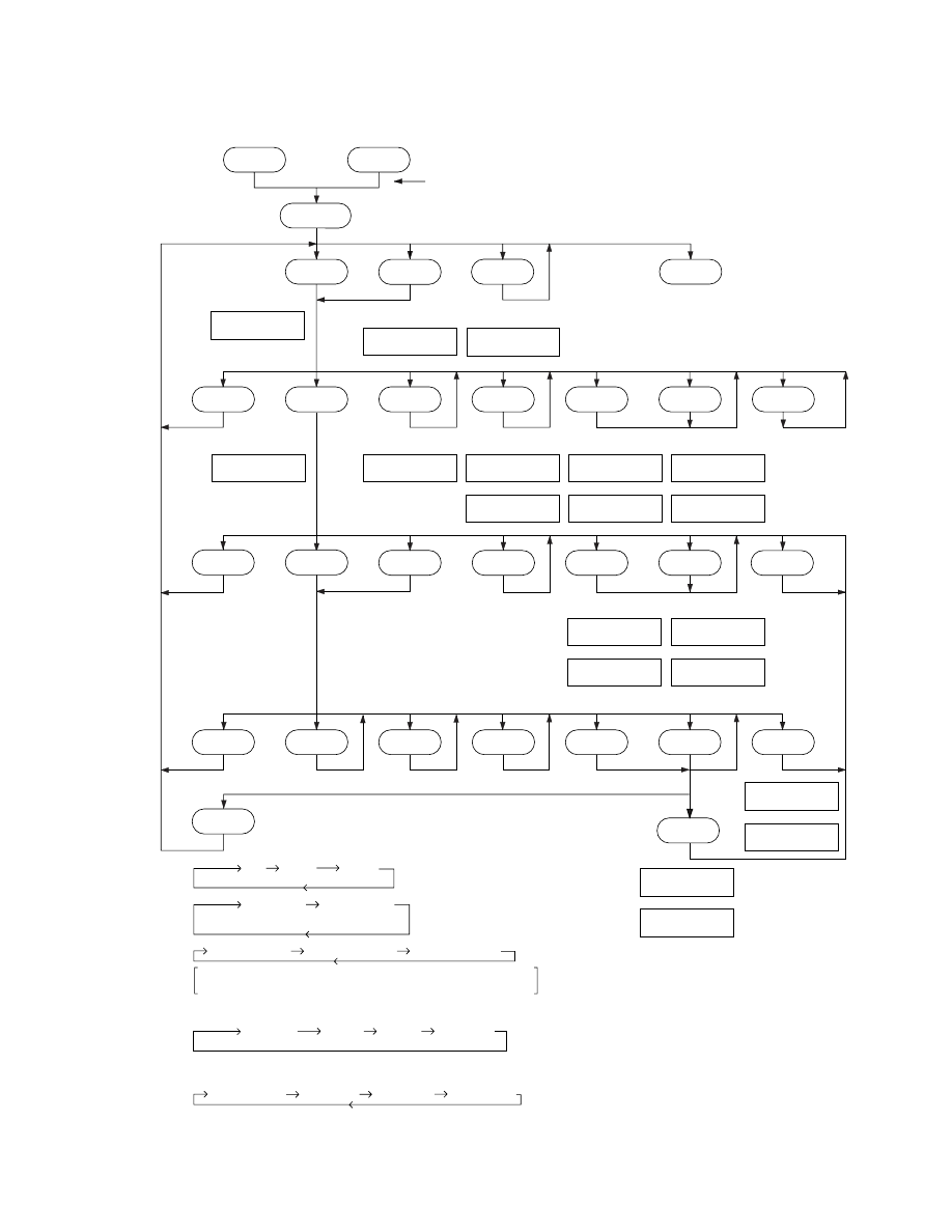
45
DEH-1000,10,1050
- Flow Chart
Focus Close
*2
S Curve Check
01 01 01
00 00 00
(99 99 99)
Display
TYP
4
3
Reset
SOURCE
New test mode
6
[
BAND
BAND
BAND
BAND
BAND
3
*2
*1
+6dB
+12dB
*4
*5
6
6
6
6
1
2
1
2
]
]
[
06 06 06
12 12 12
Sourse CD
Single TR
32TRK
92(82)
CRG Move
94(84)
100TRK
93(83)
Focus Mode
Select
Focus Close/
S Curve Check
CRG-
Auto Adjustment
Display Select
<Tracking Servo Close>
CRG+
RF AGC Coefficient Display/
Rough Servo and RF AGC
Tracking
Open
Display
Tracking
Open
T. Close and
Fit Servo
*3
F.Offset Display
RF.Offset Display
F.Cansel Display
*7
Single TR/32TR/100TR
Voltage of CRG Motor = 2 [V]
(F,T.AGC Gain = (Present Value/Initial Value) ¥ 20)
*6
]
[
1
3
Display
2
3
Display
or
8x 8x 8x
TRK
SEC
MIN
9x 9x 9x
TRK
SEC
MIN
or
CRG-
CRG+
T.Balance
Adjustment
*7
F, T, RF AGC/
F.Bias Display Select
F, T AGC and
RF AGC
CRG Move, 100TR Jump Only
TRK, MIN, SEC
F.AGC Gain
RF AGC Gain
T.AGC Gain
*8
Power ON
(Adjustment for T.Offset)
*5
*4
*4
*6
CRG/TR Jump NO.
Select
CRG+/TR Jump+
CRG-/TR Jump-
Power OFF
Display
Display
Display
T.Close and
F,T AGC and
RF AGC and
Fit Servo
Display
Power ON
(Not adjustment for T.Offset)
Display
Display
2
RF AMP Gain Select
2
Power OFF
Power OFF
Power OFF
8x 8x 8x
TRK
SEC
MIN
9x 9x 9x
TRK
SEC
MIN
8x 8x 8x
TRK
SEC
MIN
9x 9x 9x
TRK
SEC
MIN
or
8x 8x 8x
TRK
SEC
MIN
9x 9x 9x
TRK
SEC
MIN
or
00 00 00
TRK
SEC
MIN
99 99 99
TRK
SEC
MIN
or
00 00 00
TRK
SEC
MIN
99 99 99
TRK
SEC
MIN
or
00 00 00
TRK
SEC
MIN
99 99 99
TRK
SEC
MIN
or
91 91 91
TRK
SEC
MIN
0x 0x 0x
TRK
SEC
MIN
00 00 00
TRK
SEC
MIN
99 99 99
TRK
SEC
MIN
GG GG GG
TRK
SEC
MIN
Test Mode In
*1
*8
*3
*8
F.Cancel Value = {Top Rank 8bit of Set Value (7F [H] to 80 [H] ) + 128} / 4
= 63 [D] to (32 [D] ) to 00 [D]
9x(8x):91(81)
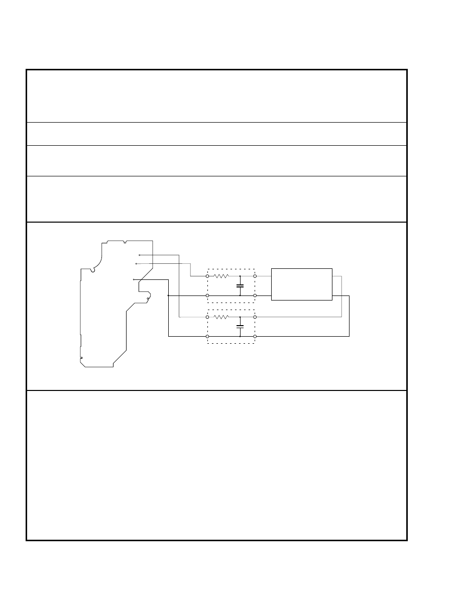
46
DEH-1000,10,1050
• Note :
The grating angle of the PU unit cannot be adjusted after the PU unit is changed. The PU unit in the CD mecha-
nism module is adjusted on the production line to match the CD mechanism module and is thus the best adjusted
PU unit for the CD mechanism module. Changing the PU unit is thus best considered as a last resort. However, if
the PU unit must be changed, the grating should be checked using the procedure below.
• Purpose :
To check that the grating is within an acceptable range.
• Symptoms of Mal-adjustment :
If the grating is off by a large amount symptoms such as being unable to close tracking, being unable to perform
track search operations, or track searching taking a long time, may appear.
• Method :
• Measuring Equipment
• Oscilloscope, Two L.P.F.
• Measuring Points
• E, F, REFOUT
• Disc
• ABEX TCD-784
• Mode
• TEST MODE
• Checking Procedure
1. In test mode, load the disc and switch the 5V regulator on.
2. Using the ] and [ buttons, move the PU unit to the innermost track.
3. Press key 3 to close focus, the display should read "91". Press key 2 to implement the tracking balance adjust-
ment the display should now read "81". Press key 3 2 times. The display will change, returning to "81" on the
fourth press.
4. As shown in the diagram above, monitor the LPF outputs using the oscilloscope and check that the phase differ-
ence is within 75° . Refer to the photographs supplied to determine the phase angle.
5. If the phase difference is determined to be greater than 75° try changing the PU unit to see if there is any
improvement. If, after trying this a number of times, the grating angle does not become less than 75° then the
mechanism should be judged to be at fault.
• Note
Because of eccentricity in the disc and a slight misalignment of the clamping center the grating waveform may be
seen to "wobble" ( the phase difference changes as the disc rotates). The angle specified above indicates the aver-
age angle.
• Hint
Reloading the disc changes the clamp position and may decrease the "wobble".
E
REFO
F
100k
Ω
390pF
100k
Ω
390pF
E
REFO
F
REFO
L.P.F.
L.P.F.
CONTROL UNIT
Xch
Ych
Oscilloscope
6.2 CHECKING THE GRATING AFTER CHANGING THE PICKUP UNIT
47
DEH-1000,10,1050
Grating waveform
Ech
→
Xch 20mV/div, AC
Fch
→
Ych 20mV/div, AC
45
°
0
°
75
°
60
°
30
°
90
°
48
DEH-1000,10,1050
7. GENERAL INFORMATION
7.1 PARTS
7.1.1 IC
- Pin Functions (PD4991A)
Pin No.
Pin Name
I/O
Function and Operation
1,2
NC
Not used
3
SYSPW
O
System power supply control output
4
NC
Not used
5
TESTIN
I
Test program mode input
6–9
NC
Not used
10
TUNPW
O
Tuner power control output
11
reset
I
Reset input
12
XT2
Not used (open)
13
XT1
Not used (GND)
14
VSS
GND
15
X2
Crystal oscillator connection pin
16
X1
Crystal oscillator connection pin
17
REGOFF
Connect to VSS
18
REGC
Capacitor for regulator connect pin
19
VDD
Power supply
20
GRNILM
O
Green illumination select output
21
NC
Not used
22
adpw
O
A/D converter power supply output
23
AMBILM
O
Amber illumination select output
24
NC
Not used
25
ASENB
O
Slave power supply control output
26,27
NC
Not used
28
MUTE
O
System mute output
29
fm/AM
O
RDS decoder power select output
30
LOCL
O
LOCL output
31
LOCH
O
LOCH output
32
TUNPCE2
O
PLL IC chip enable output
33
VCK
O
Clock output for electronic volume
34
VST
O
Strobe pulse output for electronic volume
35
VDT
O
Data output for electronic volume
36,37
NC
Not used
38
SD
I
SD input
39
st
I
FM stereo input
40
VSS
GND
41
VDD
Power supply
42–44
NC
Not used
45
currq
O
Tuner voltage FIX output
46–50
NC
Not used
51
swvdd
O
Keyboard unit power supply control output
52
dsens
I
Grille detach sense input
53
CONT
O
CD server driver power control output
54
CD5VON
O
CD +5V power control output
55
NC
Not used
56
VDCONT
O
CD VD power control output
57
CDMUTE
O
CD mute control output
58
CDEJET
O
CD eject control output
59
CDLOAD
O
CD LOAD motor loading control output
60
LOCK
I
CD spindle lock input
61
FOK
I
CD focus OK input
62
PCL
O
Clock adjustment output
63
MIRR
I
CD mirror detector input
49
DEH-1000,10,1050
IC's marked by* are MOS type.
Be careful in handling them because they are very
liable to be damaged by electrostatic induction.
*PD4991A
Pin No.
Pin Name
I/O
Function and Operation
64
clamp
I
CD disc clamp sense input
65
xsck
O
CD LSI clock output
66
XSI
I
CD LSI data input
67
XSO
O
CD LSI data output
68
XA0
O
CD LSI command/data control output
69
xrst
O
CD LSI reset output
70
xstb
O
CD LSI strobe output
71,72
NC
Not used
73
TEST
I
Test terminal
74
SL
I
Tuner signal level input
75
MODEL1
I
Model select input
76,77
NC
Not used
78
EJTSNS
I
CD disc EJECT position detect
79
DSCSNS
I
CD disc detect input
80
VDSENS
I
CD VD over voltage / short-circuit sense input
81
TEMP
I
CD temperature sense input (CD)
82
(VDD)
A/D converter power supply terminal
83
(VDD)
A/D converter reference voltage terminal
84
(GND)
A/D converter GND
85,86
NC
Not used
87
GND
GND
88
ldet
I
RDS PLL lock sense input
89–91
NC
Not used
92
asens
I
ACC power sense input
93
bsens
I
Back up power sense input
94
TUNPDI
I
PLL IC data input
95
KEYDT
I
Key data input
96
DPDT
O
Display data output
97
TUNPCK
O
PLL IC clock output
98
TUNPDO
O
PLL IC data output
99
TUNPCE
O
PLL IC chip enable
100
PEE
O
Beep tone output
30
31
50
51
80
81
100
1
50
DEH-1000,10,1050
- Pin Functions (PD6294A)
Pin No.
Pin Name
I/O
Function and Operation
1
VSS
GND
2
X1
Crystal oscillator connection pin
3
X0
Crystal oscillator connection pin
4
NC
Not used
5,6
MOD1,0
I
Connect to GND
7
NC
Not used
8
KYDT
O
Key data output
9
DPDT
I
Display data input
10
REMIN
I
Remote control pulse input
11,12
NC
Not used
13-16
kd$-kd!
I
Key data input
17-22
KST6-KST1
O
Key strobe output
23
VDD
VDD
24-73
SEG49-0
O
LCD segment output
74-77
COM3-0
O
LCD common output
78
VLCD
I
LCD voltage input
79,80
V2,V1
Power supply terminal
*PD6294A
20
21
40
41
60
61
80
1
PAL005A
1
2
3
4
5
6
7
Mute
8
9
10
11
12
13
14
15
16
17
18
19
20
21
22
23
24
25
Mute
Mute
Mute
STBY
Protector
Amp2
Amp1
Amp3
Amp4
TA
B
P-GND2
OUT2-
OUT2+
STBY
VCC
OUT1-
OUT1+
P-GND1
P-GND3
P-GND4
Switch_out
MUTE
OUT4+
OUT4-
SVR
IN1
IN2
IN4
S-GND
IN3
Ac_gnd
OUT3+
OUT3-
VCC
BR9010FV
NC
VCC
CS
SK
WC
GND
DO
DI
1
2
3
4
8
7
6
5
CS
SK
DI
DO
WC
: Chip select input
: Serial data clock input
: Serial data input
: Serial data output
: Write control input
51
DEH-1000,10,1050
1
2
3
4
5
6
7
8
9
10
11
12
13
14
15
16
17
18
19
20
21
22
23
24
25
26
27
28
Vref
IN1_L
IN2_L
IN3_L
IN4+_L
AGND Loud-
out_L
SVin_L
Front-
out_L
Rear-
out_L
FIE_L
DGND
IN4-_L
CLK
VCC
IN1_R
IN2_R
IN3_R
IN4+_R
AGND
Loud-
out_R
SVin_R
Front-
out_R
Rear-
out_R FIE_R
STB
IN4-_R
DATA
Isolator
circuit
Primary
volume
Anti Alias
filter
Treble
Anti radiation
filter
Middle
Bass
Loudness
volume
FIE
Fader
volume
Secondary
volume
Zero cross
detect circuit
Primary
volume
Anti Alias
filter
Middle
Treble
Bass
Isolator
circuit
Anti radiation
filter
Loudness
volume
Zero cross
detect circuit
Fader
volume
Secondary
volume
FIE
Digital block
Auto-Zero
Auto-Zero
PML003AM
52
DEH-1000,10,1050
- Pin Functions (UPD63710GC)
Pin No.
Pin Name
I/O
Function and Operation
1
GND
Logic circuit GND
2
HOLD
I/O
Defect detection output
3
MIRR
I/O
MIRR output
4
FOK
O
RFOK signal output
5
rst
I
Reset signal input
6
A0
I
Command/parameter identification signal input
7
stb
I
Data strobe signal input
8
sck
I
Clock signal input for serial data input/output
9
SO
O
Serial data and status signal output
10
SI
I
Serial data input
11
VDD
Positive power supply terminal to logic circuit
12
DA.VDD
Positive power supply terminal to D/A converter
13
NC
Not used
14, 15
DA.GND
D/A converter GND
16
NC
Not used
17
DA.VDD
Positive power supply terminal to D/A converter
18
R+
O
Right channel audio data output
19
R-
O
Right channel audio data output
20
L-
O
Left channel audio data output
21
L+
O
Left channel audio data output
22
X.VDD
Positive power supply terminal to crystal oscillation circuit
23
xtal
O
Crystal oscillator connect pin
24
XTAL
I
Crystal oscillator connect pin
25
X.GND
Crystal oscillation circuit GND
26
VDD
Positive power supply terminal to logic circuit
27
EMPH
O
Output pin for the pre-emphasis data in the sub-Q code
28
FLAG
O
Flag output pin to indicate that audio data currently being output consists
of noncorrectable data
29
DIN
I
Serial data input to internal DAC
30
DOUT
O
Serial audio data output
31
SCKIN
I
Serial clock input to internal DAC
32
SCKO
O
Audio data that is output from DOUT changes at rising edge of this clock
33
LRCKIN
I
LRCK signal input to internal DAC
34
LRCK
O
Signals to distinguish the right and left channels of the audio data output
from DOUT
35
WDCK
O
Output double the frequency of LRCK
36
TX
O
Digital audio interface data output
37
GND
Logic circuit GND
38
C16M
O
Oscillator clock buffering output
39
LIMIT
I
Status of the pin is output at Bit 5 of the status output
40
VDD
Positive power supply terminal to logic circuit
41
LOCK
O
EFM synchronous detection signal
42
RFCK
O
Frame synchronous signal of XTAL-system
43
WFCK
O
Frame synchronous signal of PLL-system
44
PLCK
O
Monitor pin of bit clock
45
GND
Logic circuit GND
46
C1D1
O
Output pin for indicating the C1 error correction results
47
C1D2
O
Output pin for indicating the C1 error correction results
48
C2D1
O
Output pin for indicating the C2 error correction results
49
C2D2
O
Output pin for indicating the C2 error correction results
50
C2D3
O
Output pin for indicating the C2 error correction results
51
VDD
Positive power supply terminal to logic circuit
52
PACK
O
CD-TEXT PACK synchronous signal
53
TSO
O
CD-TEXT data serial output
54
TSI
I
CD-TEXT control parameter serial input
55
tsck
I
CD-TEXT serial clock input
56
TSTB
I
CD-TEXT parameter strobe signal input
57
GND
Logic circuit GND
58
TEST
I
Test pin
53
DEH-1000,10,1050
Pin No.
Pin Name
I/O
Function and Operation
59
ATEST
I/O
Test pin
60
RFMODE
I
Use/not use select for internal RF amplifier
61
A.GND
Analog circuit GND
62
FD
O
Focus drive output
63
TD
O
Tracking drive output
64
SD
O
Sled drive output
65
MD
O
Spindle drive output
66
DACO
O
DAC output for adjustment
67
FBAL
O
DAC output for adjustment
68
TBAL
O
DAC output for adjustment
69
TEVCA
O
DAC output for adjustment
70
A.VDD
Power supply terminal to analog circuit
71
EFM
O
EFM signal output
72
ASY
I
EFM comparator reference voltage input
73
C3T
3T detection capacitor additional pin
74
RFI
I
RF signal input for EFM data regulation
75
AGCO
O
RF signal output of after gain adjustment
76
AGCI
I
RF-AGC amplifier input
77
RFO
O
RF summing amplifier output
78
EQ2
RF amplifier equalizer parts additional pin
79
EQ1
RF amplifier equalizer parts additional pin
80
RF-
I
RF summing amplifier inverted input
81
A.GND
Analog circuit GND
82
A
I
Photo detector A input
83
C
I
Photo detector C input
84
B
I
Photo detector B input
85
D
I
Photo detector D input
86
F
I
Photo detector F input
87
E
I
Photo detector E input
88
A.VDD
Positive power supply terminal to analog circuit
89
REFOUT
O
Reference electric potential output
90
FE-
I
Focus error amplifier inverted input
91
FEO
I/O
Focus error amplifier output
92
TE-
I
Tracking error amplifier inverted input
93
TEO
I/O
Tracking error amplifier output
94
TE2
I/O
Tracking error output of after amplification
95
TEC
I
Tracking comparator input
96
A.GND
Analog circuit GND
97
PD
I
PD detection signal input for LD output monitor
98
LD
O
LD control current output
99
PN
I
APC circuit control polarity set pin
100
A.VDD
Positive power supply terminal to analog circuit
20
21
40
41
60
61
80
1
100
76
26
1
25
75
51
50
*UPD63710GC
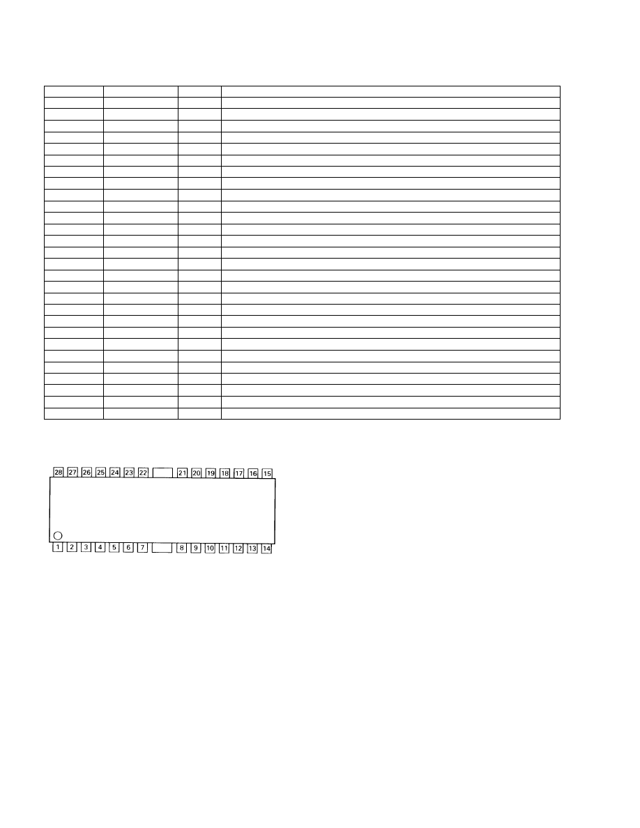
54
DEH-1000,10,1050
- Pin Functions (BA5985FM)
Pin No.
Pin Name
I/O
Function and Operation
1
FWD
I
Loading driver FWD input
2
OPIN1(
+
)
I
CH1 pre-amplifier input
3
OPIN1(
−
)
I
CH1 pre-amplifier inverted input
4
OPOUT1
O
CH1 pre-amplifier output
5
OPIN2(
+
)
I
CH2 pre-amplifier input
6
OPIN2(
−
)
I
CH2 pre-amplifier inverted input
7
OPOUT2
O
CH2 pre-amplifier output
8
VCC
Power supply
9
VOL(
−
)
O
Loading driver negative output
10
VOL(
+
)
O
Loading driver positive output
11
VO2(
−
)
O
Driver CH2 negative output
12
VO2(
+
)
O
Driver CH2 positive output
13
VO1(
−
)
O
Driver CH1 negative output
14
VO1(
+
)
O
Driver CH1 positive output
15
VO4(
+
)
O
Driver CH4 positive output
16
VO4(
−
)
O
Driver CH4 negative output
17
VO3(
+
)
O
Driver CH3 positive output
18
VO3(
−
)
O
Driver CH3 negative output
19
GND
GND
20
BIAS
I
Bias input
21
MUTE
Mute control
22
OPOUT3
O
CH3 pre-amplifier output
23
OPIN3(
−
)
I
CH3 pre-amplifier inverted input
24
OPIN3(
+
)
I
CH3 pre-amplifier input
25
OPOUT4
O
CH4 pre-amplifier output
26
OPIN4(
−
)
I
CH4 pre-amplifier inverted input
27
OPIN4(
+
)
I
CH4 pre-amplifier input
28
REV
I
Loading driver REV input
BA5985FM

55
DEH-1000,10,1050
COMMON
SEGMENT
7.1.2 DISPLAY
- CAW1500
56
DEH-1000,10,1050
7.2 DIAGNOSIS
7.2.1 DISASSEMBLY
-
Removing the Tuner Amp Unit(Fig.2)
Remove the two screws.
Remove the three screws.
Remove the screw.
Straighten the tabs at four locations indi-
cated.
Remove the Tuner Amp Unit.
-
Removing the Case Unit(not shown)
1. Remove the Case Unit.
-
Removing the Panel Assy(Fig.1)
Disengage the stoppers at two locations.
Remove the Panel Assy.
-
Removing the CD Mechanism Module
(not shown)
1. Remove the four screws.
2.Disconnect the connector, and then remove the
CD Mechanism Module.
Fig.1
Fig.2
Panel Assy
Tuner Amp Unit
57
DEH-1000,10,1050
7.2.2 TEST MODE
- Error Messages
If a CD is not operative or stopped during operation due to an error, the error mode is turned on and cause(s) of the
error is indicated with a corresponding number. This arrangement is intended at reducing nonsense calls from the
users and also for facilitating trouble analysis and repair work in servicing.
(1) Basic Indication Method
1) When SERRORM is selected for the CSMOD (CD mode area for the system), error codes are written to DMIN (min-
utes display area) and DSEC (seconds display area). The same data is written to DMIN and DSEC. DTNO remains
in blank as before.
2) Head unit display examples
Depending on display capability of LCD used, display will vary as shown below. xx contains the error number.
8-digit display
6-digit display
4-digit display
ERROR–xx
ERR–xx
E–xx
OR
Err–xx
(2) Error Code List
Code
Class
Displayed error code Description of the code and potential cause(s)
10
Electricity
Carriage Home NG
CRG can't be moved to inner diameter.
CRG can't be moved from inner diameter.
→
Failure on home switch or CRG move mechanism.
11
Electricity
Focus Servo NG
Focusing not available.
→
Stains on rear side of disc or excessive vibrations on REWRITABLE.
12
Electricity
Spindle Lock NG
Spindle not locked. Sub-code is strange (not readable).
→
Failure on spindle, stains or damages on disc, or excessive vibrations.
Subcode NG
A disc not containing CD-R data is found. Turned over disc are found,
though rarely.
→
Failure on home switch or CRG move mechanism.
RF AMP NG
An appropriate RF AMP gain can't be determined.
→
CD signal error.
17
Electricity
Setup NG
APC protection doesn't work. Focus can be easily lost.
→
Damages or stains on disc, or excessive vibrations.
30
Electricity
Search Time Out
Failed to reach target address.
→
CRG tracking error or damages on disc.
A0
System
Power Supply NG
Power (VD) is ground faulted.
→
Failure on SW transistor or power supply (failure on connector).
Remarks: Mechanical errors are not displayed (because a CD is turned off in these errors).
Unreadable TOC does not constitute an error. An intended operation continues in this case.
A newly designed head unit must conform to the example given above.
Upper digits of an error code are subdivided as shown below:
1x: Setup relevant errors, 3x: Search relevant errors, 3x: Search relevant errors, Ax: Other errors.
58
DEH-1000,10,1050
- New Test Mode
S-CD plays the same way as before.
If an error such as off focus, spindle unlocking, unreadable sub-code, or sound skipping occurs after setup, its
cause and time occurred (in absolute time) are displayed.
During setup, operational status of the control software (internal RAM: CPOINT) is displayed.
These displays and functions are prepared for enhancing aging in the servicing and efficiency of trouble analysis.
(1) Shifting to the New Test Mode
1 Turn on the current test mode by starting the reset from the key (it varies between the products).
2 Select S-CD for the source through the specified procedure including use of the [SOURCE] key, and inserting the
disc. Then, press the [Jump Mode Selector] key while maintaining the regulator turned off.
3 After the above operations, the new test mode remains on irrespective of whether the S-CD is turned on or off.
You can reset the new test mode by turning on the reset start.
* With some products, the new test mode can be reset through the same operations as that employed for shifting to
the STBY mode (while maintaining the Acc turned off).
(2) Key Correspondence
Key
Test mode
New test mode
(Example)
Power Off
Power On
In-play
Error Production
BAND
To power on
To power off
–
Time/Err.No. switching
(offset adjustment performed)
]
–
FWD-Kick
FF/TR+
–
[
–
REV-Kick
REV/TR-
–
1
–
T.Close (AGC performed)
Scan
–
/parameter display switching
2
RF AMP gain switching
Parameter display switching
Mode
–
/T.BAL adjustment/T.Open
3
To power on
F.Close/RF AGC/F.T.AGC
–
–
(offset adjustment not performed)
6
–
F.Mode switching
Auto/Manu T.No./Time switching
/T.Close (no AGC)/Jump switching
Note: Eject and CD on/off is performed in the same procedure as that for the normal mode.
(3) Cause of Error and Error Code
Code
Class
Contents
Description and cause
40
Electricity
Off focus detected.
FOK goes low.
→
Damages/stains on disc, vibrations or failure on servo.
41
Electricity
Spindle unlocked.
FOK = Low continued for 50 msec.
→
Damages/stains on disc, vibrations or failure on servo.
42
Electricity
Sub-code unreadable.
Sub-code was unreadable for 50 msec.
→
Damages/stains on disc, vibrations or failure on servo.
43
Electricity
Sound skipping detected.
Last address memory function was activated.
→
Damages/stains on disc, vibrations or failure on servo.
Note: Mechanical errors during aging are not displayed.
The error codes should be indicated in the same way as in the normal mode.
59
DEH-1000,10,1050
(4) Display of Operational Status (CPOINT) during Setup
Status No. Contents
Protective action
00
CD
+
5V ON process in progress.
None
01
Servo LSI initialization (1/3) in progress.
None
02
Servo LSI CRAM initialization in progress.
None
03
Servo LSI initialization (2/3) in progress.
None
04
Offset adjustment (1/3) in progress.
None
05
Offset adjustment (2/3) in progress.
None
06
Offset adjustment (3/3) in progress.
None
07
FZD adjustment in progress.
None
08
Servo LSI initialization (3/3) in progress.
None
10
Carriage move to home position started.
None
11
Carriage move to home position started.
None
12
Carriage is moving toward inner diameter.
Specified 10 seconds has been passed or failure
on home switch.
13
Carriage is moving toward outer diameter.
Specified 10 seconds has been passed or failure
on home switch.
14
Carriage outer kick in progress.
None
15
Carriage outer diameter feed (1 second) in progress.
None
20
Servo close started.
None
21
Pre-processing for focus search started.
None
22
Spindle rotation and focus search started.
None
23
Waiting for focus close (XSI
=
Low).
Specified focus search time has been passed.
24
Standing by after focus close is over.
Specified focus search time has been passed.
25
Focus search preprocessing is in
None
progress while setup protection is turned on.
26
Focus search preprocessing is in
None
progress while focus recovery is turned on.
27
Wait time after focus close is set up.
Off focus.
28
Standing by after focus close is over.
Off focus.
29
Setup (1/2) before T balance adjustment is started.
Off focus.
30
Setup (2/2) before T balance adjustment is started.
Off focus.
31
T balance adjustment started.
Off focus.
32
T balance adjustment (1/2).
Off focus.
33
T balance adjustment (2/2).
Off focus.
34
Waiting for spindle rotation to end.
Off focus.
Spindle rough servo.
35
Standing by after spindle rough servo is over.
Off focus.
36
RF AGC started.
Off focus.
37
RF AGC started.
Off focus.
38
RF AGC ending process in progress.
Off focus.
39
Tracking close in progress.
Off focus.
40
Standing by after tracking is closed.
Off focus.
Carriage closing in progress.
41
Focus/tracking AGC started.
Off focus.
42
Focus AGC started.
Off focus.
43
Focus AGC in progress.
Off focus.
44
Tracking AGC in progress.
Off focus.
45
Standing by after focus/tracking AGC are over.
Off focus.
46
Spindle processes applicable servo.
Off focus.
47
Check for servo close is started.
Off focus.
48
Check of LOCK pin started.
Off focus or spindle not locked.
49
RF AGC started.
Off focus.
50
RF AGC in progress.
Off focus.
51
Standing by after RF AGC is over.
Off focus.

60
DEH-1000,10,1050
(5) Display Examples
1) During Setup (When status no. = 11)
TRK No.
MIN.
SEC.
11
11'
11"
2) During Operation (TOC read, TRK search, Play, FF and REV)
The same as in the normal mode.
3) When a Protection Error Occurred
Switch to the following displays (A) and (B) using the [BAND] switch:
(A) Error occurrence timing display in absolute time.
An example: Error occurred in 12th tune at 34'56" in absolute time.
TRK No.
MIN.
SEC.
12
34'
56"
(B) Error No. display
An example: Error #40 (Off focus is detected)
ERROR-40
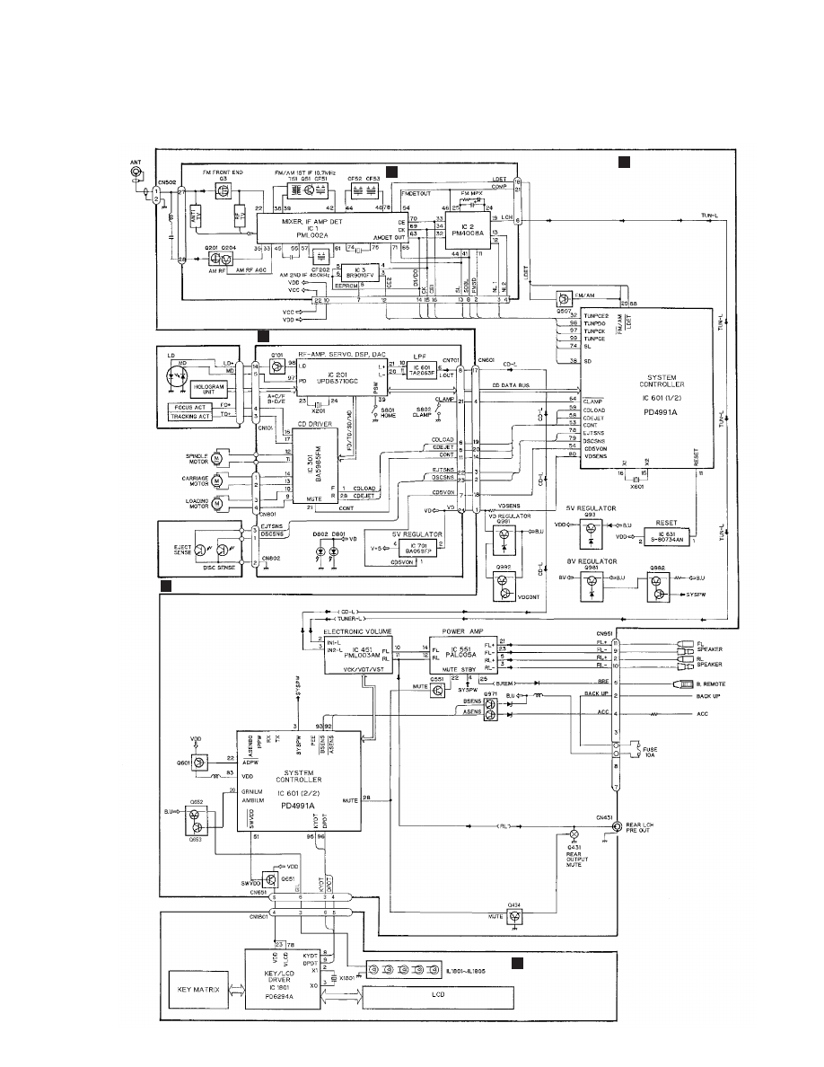
61
DEH-1000,10,1050
7.3 BLOCK DIAGRAM
A
TUNER AMP UNIT
B
FM/AM TUNER UNIT
D
CONTROL UNIT
PICKUP UNIT(SERVICE)
PHOTO UNIT
E
KEYBOARD UNIT
C
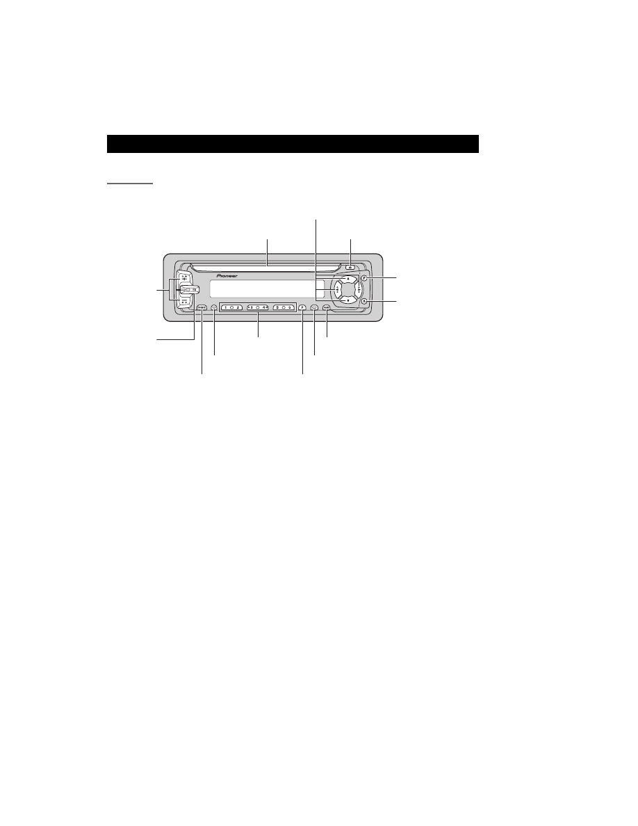
62
DEH-1000,10,1050
8. OPERATIONS AND SPECIFICATIONS
8.1 OPERATIONS
Key Finder
Head Unit
CLOCK button
Buttons 1 – 6
PGM button
EJECT button
Disc loading slot
AUDIO button
5/∞/2/3 buttons
FUNCTION button
SOURCE button
+/– button
BAND button
LOUD button
EQ button
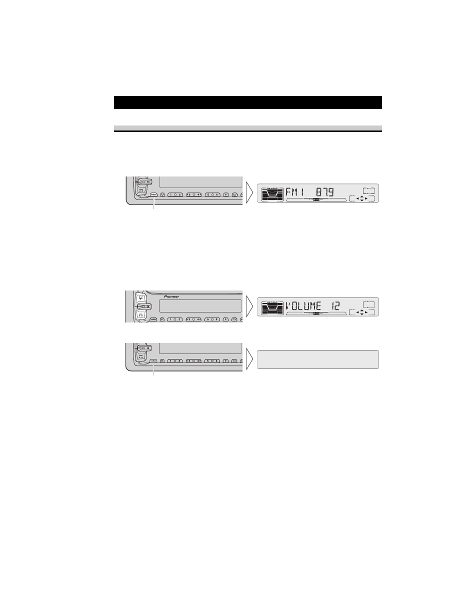
63
DEH-1000,10,1050
Basic Operation
To Listen to Music
The following explains the initial operations required before you can listen to music.
Note:
• Loading a disc in this product.
1. Select the desired source (e.g. tuner).
7 Head Unit
Each press of the SOURCE button selects the desired source in the following order:
Built-in CD player
= Tuner
Note:
• The sound source will not change if no disc is set in this product.
Each press changes the Source ...
2. Raise or lower the volume.
3. Source OFF.
Hold for 1 second or more
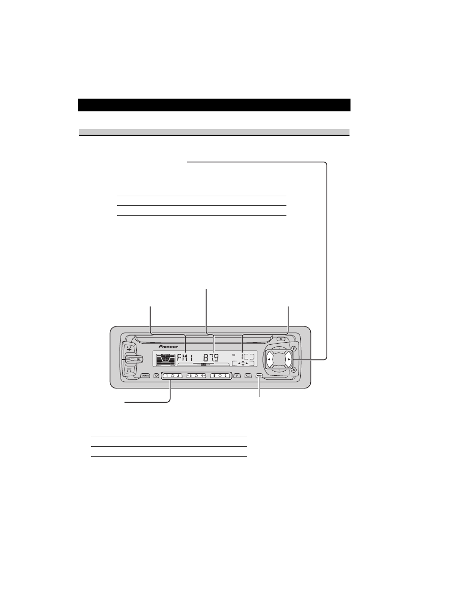
64
DEH-1000,10,1050
Basic Operation
Basic Operation of Tuner
Manual and Seek Tuning
• You can select the tuning method by changing the length of
time you press the
2/3 button.
Manual Tuning (step by step)
0.5 seconds or less
Seek Tuning
0.5 seconds or more
Note:
• If you continue pressing the button for longer than 0.5 seconds, you can
skip broadcasting stations. Seek Tuning starts as soon as you stop pressing
the button.
• “” stereo indicator lights when a stereo station is selected.
Preset Tuning
• You can memorize broadcast stations in buttons
1 through 6 for easy, one-touch station recall.
Preset station recall
2 seconds or less
Broadcast station preset memory
2 seconds or more
Note:
• Up to 18 FM stations (6 in FM1, FM2 and FM3) and 6 AM
stations can be stored in memory.
• You can also use the
5 or ∞ buttons to recall broadcast
stations memorized in buttons 1 through 6.
Preset Number Indicator
Band Indicator
Band
FM 1
= FM 2 = FM 3
= AM
Frequency Indicator
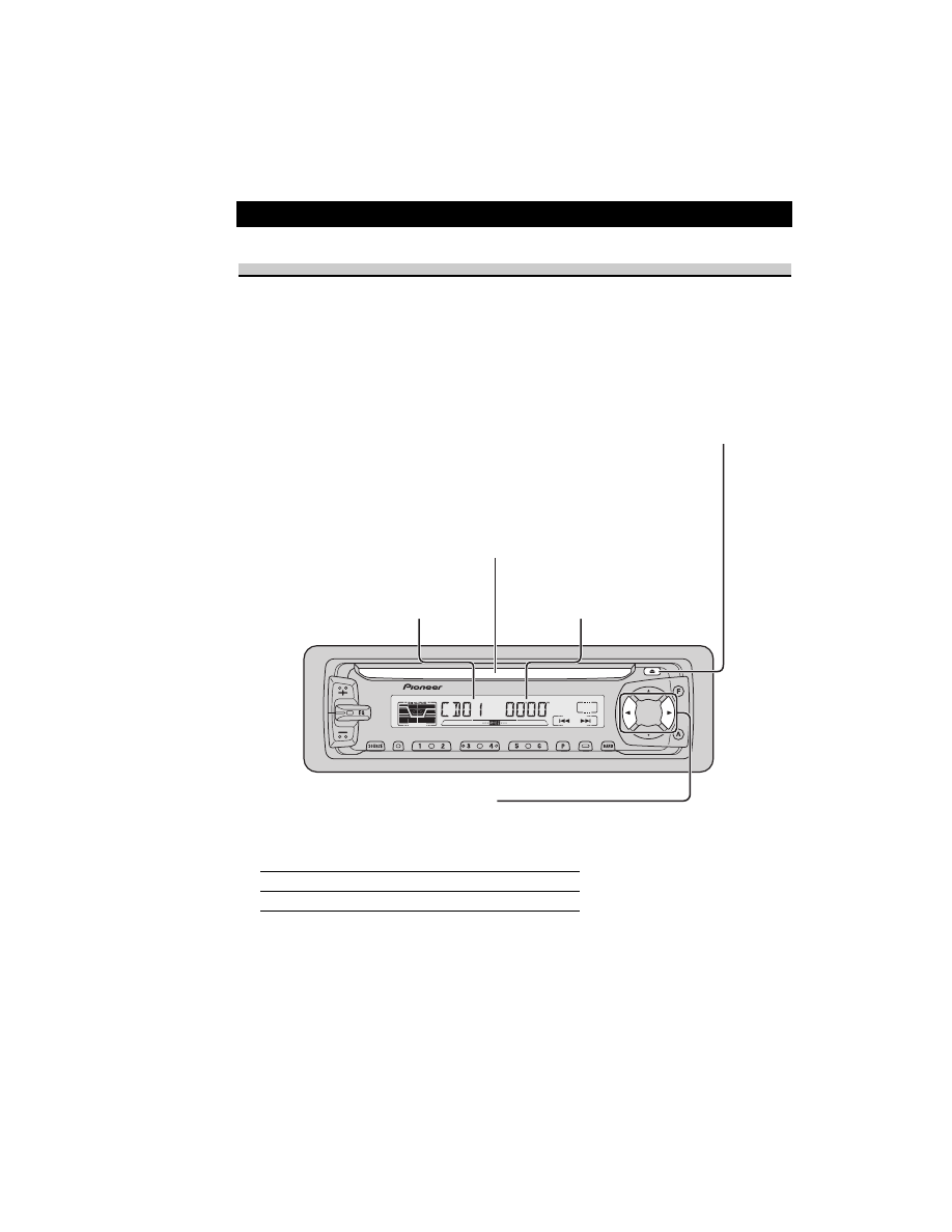
65
DEH-1000,10,1050
Basic Operation of Built-in CD Player
Track Search and Fast Forward/Reverse
• You can select between Track Search or Fast forward/Reverse by pressing
the
2/3 button for a different length of time.
Track Search
0.5 seconds or less
Fast forward/Reverse
Continue pressing
Note:
• If a disc cannot be inserted fully or playback fails, make sure the recorded side is down. Push the
EJECT button and check the disc for damage before reinserting it.
• If a CD is inserted with the recorded side up, it will be ejected automatically after a few moments.
• If the built-in CD player cannot operate properly, an error message (such as “ERROR-14”) appears
on the display.
Disc Loading Slot
The built-in CD player plays one standard 12 cm or 8 cm (single)
CD at a time. Do not use an adapter when playing 8 cm CD.
Eject
Note:
• The CD function can be turned
ON/OFF with the disc remaining in
this product.
• Discs left partially inserted after ejec-
tion may incur damage or fall out.
Elapsed Play Time Indicator
Track Number Indicator
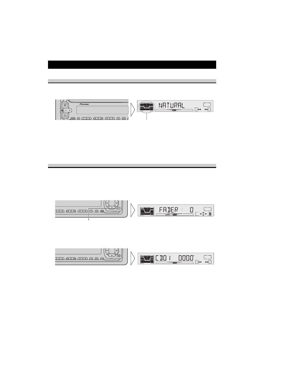
66
DEH-1000,10,1050
Audio Adjustment
Selecting the Equalizer Curve
You can switch between Equalizer curves.
•
Move the EQ button up or down to select the desired Equalizer curve.
POWERFUL
+
= NATURAL +
= VOCAL +
= CUSTOM +
= EQ FLAT
+
= SUPER BASS
Note:
• “CUSTOM” stores an equalizer curve you have made adjustments to.
• You can create different “CUSTOM” curves for different sources.
Entering the Audio Menu
With this Menu, you can adjust the sound quality.
Note:
• After entering the Audio Menu, if you do not perform an operation within about 30 seconds, the
Audio Menu is automatically canceled.
1. Select the desired mode in the Audio Menu.
2. Operate a mode.
3. Cancel the Audio Menu.
Each press changes the Mode ...
Equalizer curve
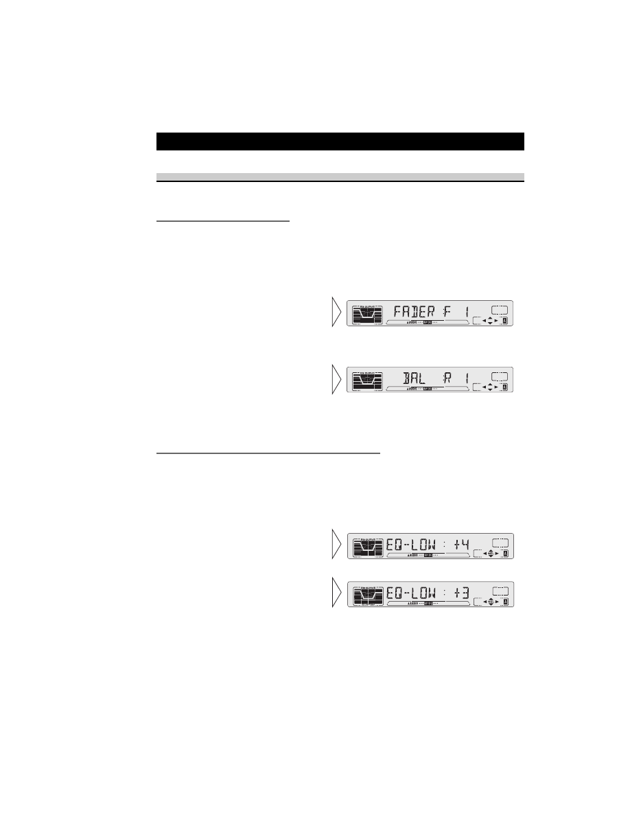
67
DEH-1000,10,1050
Audio Adjustment
Audio Menu Functions
The Audio Menu features the following functions.
Balance Adjustment (FADER)
This function allows you to select a Fader/Balance setting that provides ideal listening con-
ditions in all occupied seats.
1. Press the AUDIO button and select Fader/Balance mode (FADER) in the
Audio Menu.
Note:
• “FADER 0” is the proper setting when 2 speakers are in use.
Equalizer Curve Adjustment (EQ-LOW/MID/HIGH)
You can adjust equalizer curve settings as desired. Adjusted equalizer curve settings are
memorized in “CUSTOM”.
1. Press the AUDIO button and select the Equalizer mode
(EQ-LOW/MID/HIGH) in the Audio Menu.
Note:
• If you make adjustments when a curve other than “CUSTOM” is selected, the adjusted curve is
stored in memory as a “CUSTOM” curve. Also, the displayed curve switches to that selected before
adjustments were made.
3. Boost or attenuate the selected
band with the
5/∞ buttons.
The display shows “+6” – “–6”.
2. Select the band you want to
adjust with the
2/3 buttons.
EQ-LOW
+
= EQ-MID +
= EQ-HIGH
3. Adjust left/right speaker bal-
ance with the
2/3 buttons.
“BAL L 9” – “BAL R 9” is displayed
as it moves from left to right.
2. Adjust front/rear speaker bal-
ance with the
5/∞ buttons.
“FADER F15” – “FADER R15” is
displayed as it moves from front to
rear.
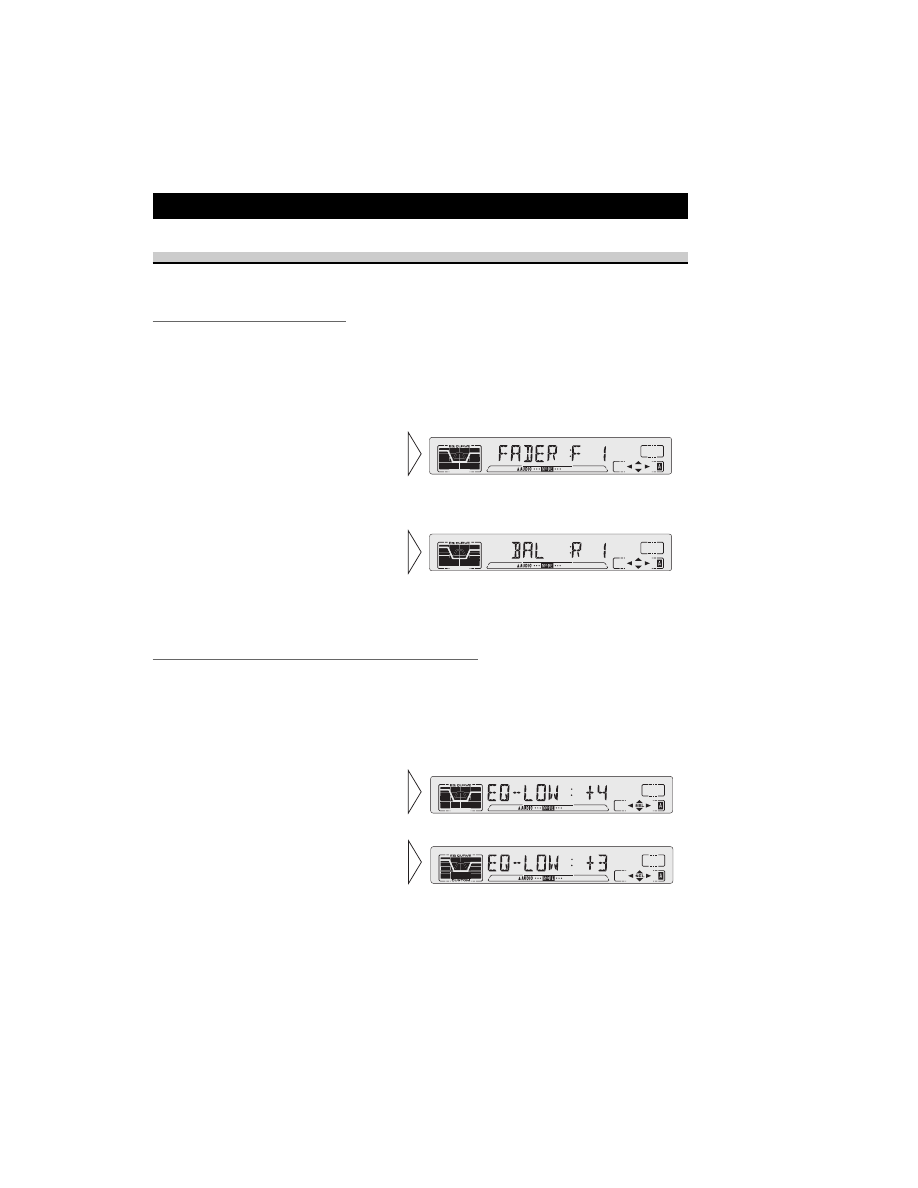
68
DEH-1000,10,1050
Audio Menu Functions
The Audio Menu features the following functions.
Balance Adjustment (FADER)
This function allows you to select a Fader/Balance setting that provides ideal listening con-
ditions in all occupied seats.
1. Press the AUDIO button and select Fader/Balance mode (FADER) in the
Audio Menu.
Note:
• “FADER 0” is the proper setting when 2 speakers are in use.
Equalizer Curve Adjustment (EQ-LOW/MID/HIGH)
You can adjust equalizer curve settings as desired. Adjusted equalizer curve settings are
memorized in “CUSTOM”.
1. Press the AUDIO button and select the Equalizer mode
(EQ-LOW/MID/HIGH) in the Audio Menu.
Note:
• If you make adjustments when a curve other than “CUSTOM” is selected, the adjusted curve is
stored in memory as a “CUSTOM” curve. Also, the displayed curve switches to that selected before
adjustments were made.
3. Boost or attenuate the selected
band with the
5/∞ buttons.
The display shows “+6” – “–6”.
2. Select the band you want to
adjust with the
2/3 buttons.
EQ-LOW
+
= EQ-MID +
= EQ-HIGH
3. Adjust left/right speaker bal-
ance with the
2/3 buttons.
“BAL L 9” – “BAL R 9” is displayed
as it moves from left to right.
2. Adjust front/rear speaker bal-
ance with the
5/∞ buttons.
“FADER F15” – “FADER R15” is
displayed as it moves from front to
rear.
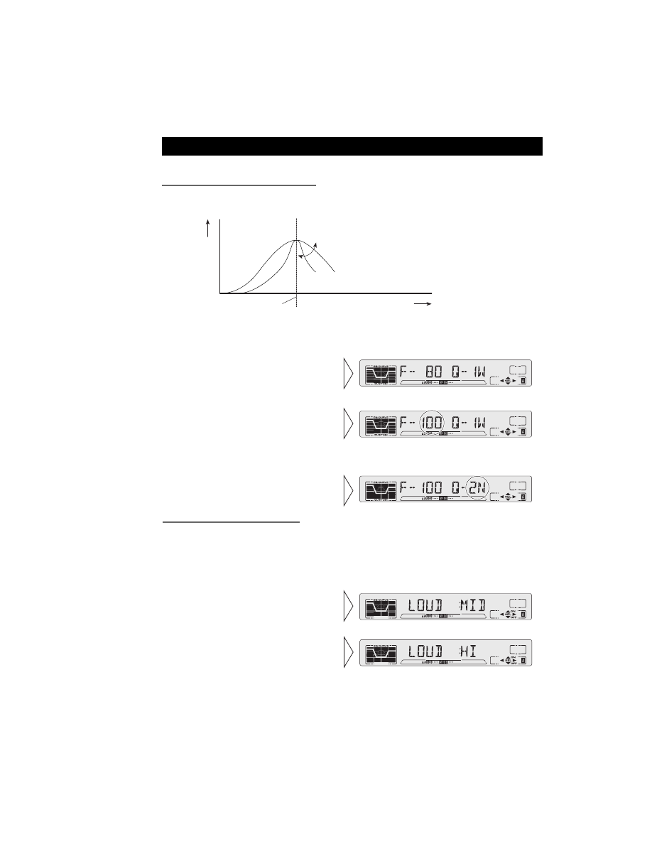
69
DEH-1000,10,1050
Equalizer Curve Fine Adjustment
You can adjust the center frequency of each equalizer curve band (LOW/MID/HIGH) and
the Q factor (curve characteristics).
1. Press the AUDIO button for 2 or more seconds to select Equalizer Curve
Fine Adjustment.
Loudness Adjustment (LOUD)
The Loudness function compensates for deficiencies in the low and high sound ranges at
low volume. You can select a desired Loudness level.
1. Press the AUDIO button and select the Loudness mode (LOUD) in the Audio
Menu.
Note:
• You can also switch the Loudness function ON/OFF by pressing the LOUD button. However,
you cannot change the level.
3. Select the desired level with the
2/3 buttons.
LOW
+
= MID +
= HI
2. Switch the Loudness function
ON/OFF with the
5/∞ buttons.
4. Select the desired Q factor with
the
5/∞ buttons.
2N
+
= 1N +
= 1W +
= 2W
3. Select the desired frequency
with the
2/3 buttons.
LOW: 40
+= 80 += 100 += 160 (Hz)
MID: 200
+= 500 += 1K += 2K (Hz)
HIGH: 3K
+= 8K += 10K += 12K (Hz)
2. Press the AUDIO button to
select the desired band for
adjustment.
Level (dB)
Q=2W
Q=2N
Center frequency
Frequency (Hz)
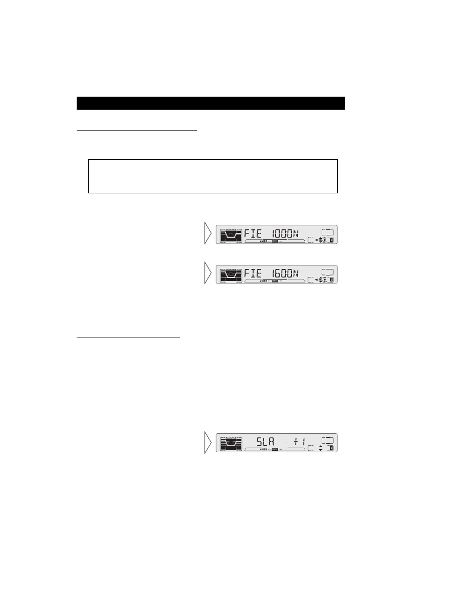
70
DEH-1000,10,1050
Audio Adjustment
Front Image Enhancer Function (FIE)
The F.I.E. (Front Image Enhancer) function is a simple method of enhancing front imaging
by cutting mid- and high-range frequency output from the rear speakers, limiting their out-
put to low-range frequencies. You can select the frequency you want to cut.
1. Press the AUDIO button and select the F.I.E. mode (FIE) in the Audio Menu.
Note:
• After switching the F.I.E. function ON, select the Fader/Balance mode in the Audio Menu, and
adjust front and rear speaker volume levels until they are balanced.
• Switch the F.I.E. function OFF when using a 2-speaker system.
Source Level Adjustment (SLA)
The SLA (Source Level Ajustment) function prevents radical leaps in volume when
switching between sources. Settings are based on the FM volume, which remains
unchanged. (Since the FM volume is the control, SLA is not possible in the FM modes.)
The AM and CD levels can all be adjusted.
1. Compare the FM volume with the volume of the other source.
(e.g. Built-in CD player)
2. Press the AUDIO button, and select the SLA mode (SLA) in the Audio
Menu.
3. Increase or decrease the level
with the
5/∞ buttons.
The display shows “+4” – “–4”.
3. Select the desired frequency
with the
2/3 buttons.
100
+
= 160 +
= 250 (Hz)
2. Switch the F.I.E. function
ON/OFF with the
5/∞ buttons.
Precaution:
• When the F.I.E. function is deactivated, the rear speakers output sound of all frequencies, not just
bass sounds. Reduce the volume before disengaging F.I.E. to prevent a sudden increase in vol-
ume.
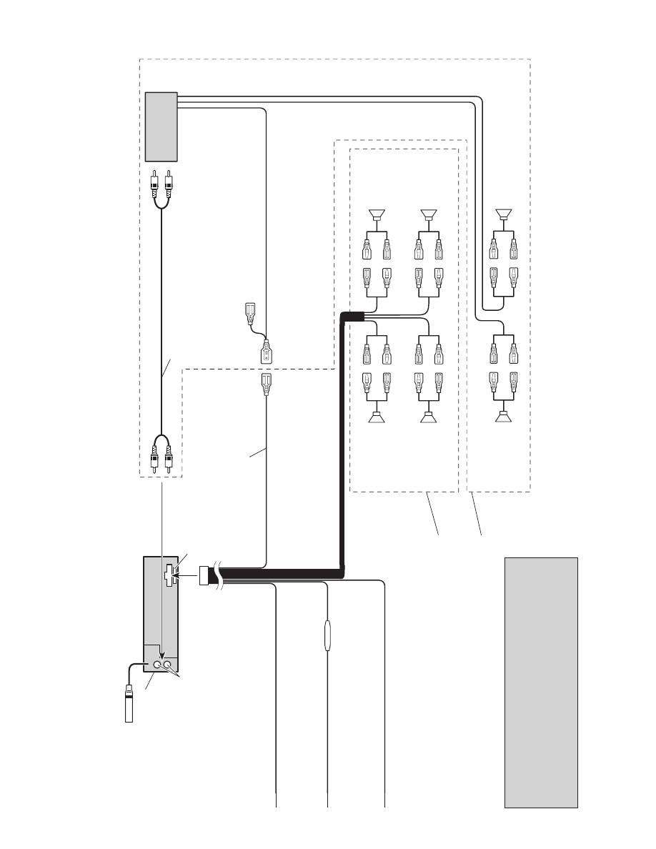
71
DEH-1000,10,1050
+
≠
+
≠
+
≠
+
≠
+
≠
+
≠
Rear
output
This
Product
Antenna
jack
Blue/white
T
o
system
control
terminal
of
the
power
amp
or
Auto-antenna
relay
control
terminal.
(Max.
300
mA
12
V
DC.)
Fuse
Connecting
cords
with
RCA
pin
plugs
(sold
separately)
Fuse
resistor
System
remote
control
Rear
speaker
Rear
speaker
Right
Front
speaker
Rear
speaker
White
Gray
White/black
Green
Green/black
Gray/black
V
iolet
V
iolet/black
Front
speaker
Rear
speaker
Left
Perform
these
connections
when
using
a
dif
ferent
amp
(sold
separately).
W
ith
a
2
speaker
system,
d
o
not
connect
anything
to
the
speaker
leads
that
are
not
connected
to
speakers.
Note:
The
electrical
leads
of
this
product
may
b
e
dif
ferent
colors
to
the
corresponding
leads
(i.e.
the
leads
that
serve
the
same
function)
of
other
products.
When
connecting
this
product
to
another
product,
please
read
the
instruction
manual
for
each
product
carefully
and
then
connect
each
lead
of
this
product
to
the
other
product
that
serves
the
same
function.
Y
ellow
T
o
terminal
always
supplied
with
power
regardless
of
ignition
switch
position.
Black
(ground)
T
o
vehicle
(metal)
body
.
Red
T
o
electric
terminal
controlled
by
ignition
switch
(12
V
DC)
ON/OFF
.
Power
amp
(sold
separately)

72
DEH-1000,10,1050
8.2 SPECIFICATIONS
- DEH-1000/X1N/UC, DEH-10/X1N/UC
General
Power source .......... 14.4 V DC (10.8 – 15.1 V allowable)
Grounding system ........................................ Negative type
Max. current consumption ...................................... 10.0 A
Dimensions
(DIN) (chassis) ...... 178 (W)
×
50 (H)
×
159 (D) mm
[7 (W)
×
2 (H)
×
6-1/4 (D) in]
(nose) ............ 188 (W)
×
58 (H)
×
19 (D) mm
[7-3/8 (W)
×
2-1/4 (H)
×
3/4 (D) in]
(D)
(chassis) ...... 178 (W)
×
50 (H)
×
164 (D) mm
[7 (W)
×
2 (H)
×
6-1/2 (D) in]
(nose) ............ 170 (W)
×
46 (H)
×
14 (D) mm
[6-3/4 (W)
×
1-3/4 (H)
×
5/8 (D) in]
Weight ........................................................ 1.4 kg (3.1 lbs)
Amplifier
Continuous power output is 22 W per channel min. into 4
ohms, both channels driven 50 to 15,000 Hz with no more
than 5% THD.
Maximum power output ...................................... 45 W
×
4
Load impedance .......................... 4
Ω
(4 – 8
Ω
allowable)
Preout maximum output
level/output impedance ............................ 2.2 V/1 k
Ω
Equalizer (3-Band Parametric Equalizer)
(Low) .......................... Frequency: 40/80/100/160 Hz
Q Factor: 0.35/0.59/0.95/1.15
(+6 dB when boosted)
Level: ±12 dB
(Mid) .......................... Frequency: 200/500/1k/2k Hz
Q Factor: 0.35/0.59/0.95/1.15
(+6 dB when boosted)
Level: ±12 dB
(High) ................ Frequency: 3.15k/8k/10k/12.5k Hz
Q Factor: 0.35/0.59/0.95/1.15
(+6 dB when boosted)
Level: ±12 dB
Loudness contour
(Low) .................. +3.5 dB (100 Hz), +3 dB (10 kHz)
(Mid) ................ +10 dB (100 Hz), +6.5 dB (10 kHz)
(High) ................ +11 dB (100 Hz), +11 dB (10 kHz)
(volume: –30 dB)
CD player
System .................................... Compact disc audio system
Usable discs .................................................. Compact disc
Signal format .................... Sampling frequency: 44.1 kHz
Number of quantization bits: 16; linear
Frequency characteristics .............. 5 – 20,000 Hz (±1 dB)
Signal-to-noise ratio ...... 94 dB (1 kHz) (IHF-A network)
Dynamic range ............................................ 92 dB (1 kHz)
Number of channels ............................................ 2 (stereo)
FM tuner
Frequency range .................................... 87.9 – 107.9 MHz
Usable sensitivity .................................................... 10 dBf
(1.0
µ
V/75
Ω
, mono, S/N: 30 dB)
50 dB quieting sensitivity .... 15 dBf (1.7
µ
V/75
Ω
, mono)
Signal-to-noise ratio ...................... 70 dB (IHF-A network)
Distortion .......................... 0.3% (at 65 dBf, 1 kHz, stereo)
Frequency response ...................... 30 – 15,000 Hz (±3 dB)
Stereo separation .......................... 40 dB (at 65 dBf, 1 kHz)
Selectivity .................................................... 70 dB (2ACA)
Three-signal intermodulation
(desired signal level) ........................................ 30 dBf
(two undesired signal level: 100 dBf)
AM tuner
Frequency range ...................................... 530 – 1,710 kHz
Usable sensitivity .............................. 18
µ
V (S/N: 20 dB)
Selectivity ................................................ 50 dB (±10 kHz)
Note:
• Specifications and the design are subject to possi-
ble modification without notice due to improve-
ments.

73
DEH-1000,10,1050
- DEH-1050/X1N/ES
General
Power source .......... 14.4 V DC (10.8 – 15.1 V allowable)
Grounding system ........................................ Negative type
Max. current consumption ...................................... 10.0 A
Dimensions
(DIN) (chassis) ...... 178 (W)
×
50 (H)
×
159 (D) mm
(nose) ............ 188 (W)
×
58 (H)
×
19 (D) mm
(D)
(chassis) ...... 178 (W)
×
50 (H)
×
164 (D) mm
(nose) ............ 170 (W)
×
46 (H)
×
14 (D) mm
Weight ...................................................................... 1.4 kg
Amplifier
Continuous power output is 22 W per channel min. into 4
ohms, both channels driven 50 to 15,000 Hz with no more
than 5% THD.
Maximum power output ...................................... 45 W
×
4
Load impedance .......................... 4
Ω
(4 – 8
Ω
allowable)
Preout maximum output level/
output impedance .................................... 2.2 V/1 k
Ω
Equalizer (3-Band Parametric Equalizer)
(Low) .......................... Frequency: 40/80/100/160 Hz
Q Factor: 0.35/0.59/0.95/1.15
(+6 dB when boosted)
Level: ±12 dB
(Mid) .......................... Frequency: 200/500/1k/2k Hz
Q Factor: 0.35/0.59/0.95/1.15
(+6 dB when boosted)
Level: ±12 dB
(High) ................ Frequency: 3.15k/8k/10k/12.5k Hz
Q Factor: 0.35/0.59/0.95/1.15
(+6 dB when boosted)
Level: ±12 dB
Loudness contour
(Low) ..................+3.5 dB (100 Hz), +3 dB (10 kHz)
(Mid) ..................+10 dB (100 Hz), +6.5 dB (10 kHz)
(High) ..................+11 dB (100 Hz), +11 dB (10 kHz)
(volume: –30 dB)
CD player
System .................................... Compact disc audio system
Usable discs .................................................. Compact disc
Signal format .................... Sampling frequency: 44.1 kHz
Number of quantization bits: 16; linear
Frequency characteristics .............. 5 – 20,000 Hz (±1 dB)
Signal-to-noise ratio ...... 94 dB (1 kHz) (IEC-A network)
Dynamic range ............................................ 92 dB (1 kHz)
Number of channels ............................................ 2 (stereo)
FM tuner
Frequency range ...................................... 87.5 – 108 MHz
Usable sensitivity
.................. 10 dBf (1.0
µ
V/75
Ω
, mono, S/N: 30 dB)
50 dB quieting sensitivity .... 15 dBf (1.7
µ
V/75
Ω
, mono)
Signal-to-noise ratio ...................... 70 dB (IEC-A network)
Distortion .......................... 0.3% (at 65 dBf, 1 kHz, stereo)
Frequency response ...................... 30 – 15,000 Hz (±3 dB)
Stereo separation .......................... 40 dB (at 65 dBf, 1 kHz)
AM tuner
Frequency range ........................ 531 – 1,602 kHz (9 kHz)
530 – 1,710 kHz (10 kHz)
Usable sensitivity .............................. 18
µ
V (S/N: 20 dB)
Selectivity .................................................. 50 dB (±9 kHz)
50 dB (±10 kHz)
Note:
• Specifications and the design are subject to possi-
ble modification without notice due to improve-
ments.
Wyszukiwarka
Podobne podstrony:
10 pyt od 901 do 1000, Nieruchomości, Nieruchomości - pośrednik
1000 years apart 1 10 PL
Make 1000$ in 10 days
10 Metody otrzymywania zwierzat transgenicznychid 10950 ppt
10 dźwigniaid 10541 ppt
wyklad 10 MNE
Kosci, kregoslup 28[1][1][1] 10 06 dla studentow
10 budowa i rozwój OUN
10 Hist BNid 10866 ppt
POKREWIEŃSTWO I INBRED 22 4 10
Prezentacja JMichalska PSP w obliczu zagrozen cywilizacyjn 10 2007
Mat 10 Ceramika
BLS 10
więcej podobnych podstron